This document summarizes Quest's capabilities for manufacturing printed circuit boards. It lists their commitment to 7 vertical markets and describes their global footprint across existing offices in Europe, Singapore, Sri Lanka, Middle East, India, and China. It also provides details on their product and service offerings including layer counts, board sizes, materials, design features, and production processes. Tables outline their process capabilities for layer registration, minimum line widths, hole sizes, surface finishes, electrical testing parameters and more.


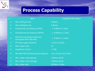
![s/n Item Capability description
1 Layers count 1- 36 layers
2 Finished Board Thickness 16~134mil(0.4mm – 3.4mm)
3 Max. panel size 21.5” × 24.5” ( 622mm × 546mm )
4 Available Laminates Material
FR-4, CEM-1,CEM-3, Aluminum-based, High Frequency, High
Tg, High CTI,Teflon, Halogen Free. Lead free compatible
5 Finished board Thickness tolerance
≤1.0mm ±0.10mm (±4mil) 1.0~1.6mm ±0.15mm
(6mil)
6 Inner thin core Min. thickness 4mil (0.10mm)
7 Min. Inner Line Width/Spacing 3/3mil (0.075/0.075mm)
8 Min. outer Line width/spacing
3/3mil (0.075/0.075mm)[for gold plating PCB]; 4/4mil
(0.10/0.10mm)[for HASL PCB];
9 Layer-layer registration tolerance ± 2mil (± 0.05mm )
10 Copper foil thickness 12u,18u, 35u, 70 u, 105u, 140u, 175u, 210u (1/3oz-6oz)
11 Min. finished hole size 0.15mm (6mil)
Process Capability](https://image.slidesharecdn.com/questpcb-140613025317-phpapp01/85/Quest-pcb-9-320.jpg)