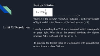
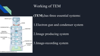
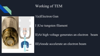
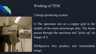
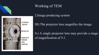
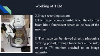
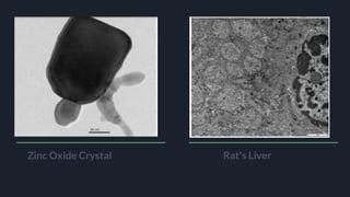
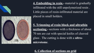
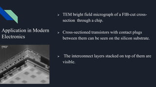
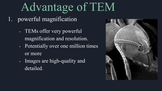
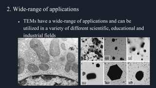
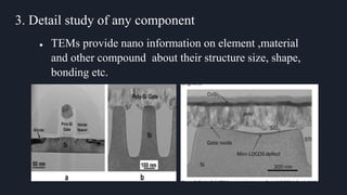
Transmission Electron Microscope(TEM)
Presented By:
Bishnu K.C(074MSMSE003)
Bishwas Pokharel(074MSMSE004)
OPTICAL MICROSCOPE WAS ALREADY THERE SO WHY TEM ??
Limit Of Resolution
Def: The resolution of an optical microscope is defined as the
shortest distance between two points on a specimen that can still
be distinguished by the observer or camera system as separate
entities.
Limit Of Resolution
If two objects are closer together than your resolution, then they
blur together in the microscope image and it's impossible to tell
that they are two points.
Q. What causes the blur in the image?
Diffraction causing blurring of the image.
Limit Of Resolution
Limit Of Resolution
Rayleigh Criterion: Images of two point objects will be
resolved when the central maximum in the diffraction pattern of
one image coincides with the first minimum of the diffraction
pattern of the other image.
Limit Of Resolution
Rayleigh Criterion:
………………………(1)
where θ is the angular resolution (radians), λ is the wavelength
of light, and D is the diameter of the lens' aperture(NA)
Usually a wavelength of 550 nm is assumed, which corresponds
to green light. With air as the external medium, the highest
practical NA is 0.95, and with oil, up to 1.5.
In practice the lowest value of d obtainable with conventional
optical lenses is about 200 nm.
Limit Of Resolution
The equation (1) shows that for better resolution the value of
a. wavelength must be small as possible
b. aperture must be large as possible( the highest
practical NA is 0.95)
So, for better resolution wavelength is the subject of interest.
Later,
In 1929 Prince Louis-Victor de Broglie was awarded the Nobel
Prize for Physics for “his discovery of the wave nature of
electrons”
Isn’t this turning point for resolution ?
Limit Of Resolution
Louis de Broglie’s famous equation shows that the wavelength
of electrons is related to their energy, E as
……………………..(2)
In this equation E is in electron volts (eV) and wavelenght in nm.
So from equation (2) you can work out that for a 100 keV
electron, λ ~ 4 pm (0.004 nm), which is much smaller than the
diameter of an atom.
From this equation, It can be concluded that at electron can be
used for better resolution(around 0.2nm) with no doubt and it’s
the origin for electron microscope.
How TEM works?
Working of TEM
(TEM),has three essential systems:
1.Electron gun and condenser system
2.Image producing system
3.Image-recording system
Working of TEM
1(a)Electron Gun
I )Use tungsten filament
II)At high voltage generates an electron beam
III)Anode accelerate an electron beam
Working of TEM
1(b)Condenser System
I)An electromagnetic coil (first lens)
concentrates the electrons into a more powerful
beam.
II)Another electromagnetic coil (the second
lens) focuses the beam onto a certain part of the
specimen.
Working of TEM
2.Image producing system
I) The specimen sits on a copper grid in the
middle of the main microscope tube. The beam
passes through the specimen and "picks up" an
image of it.
II)Objective lens produce real intermediate
image.
Working of TEM
2.Image producing system
III) The projector lens magnifies the image.
Iv) A single projector lens may provide a range
of magnification of 5:1
Is Diffraction occurs in TEM ?
Yes, it helps to determine the
I)Specimen thickness
II)Crystal Structure
III) Crystal Symmetry etc..
Working of TEM
3.Image recording system
I)The image becomes visible when the electron
beam hits a fluorescent screen at the base of the
machine.
II)The image can be viewed directly (through a
viewing portal), through binoculars at the side,
or on a TV monitor attached to an image
intensifier
Zinc Oxide Crystal Rat’s Liver
1. Fixation - fixed with chemical products , can be achieved by perfusion and
microinjection, immersions, or with vapours using various fixatives (chemicals
that denature and precipitate cellular macromolecules) eg: aldehydes tannic acid,
or thiocarbohydrazide.
2. Rinsing and ‘staining’ - treated with heavy metal compounds (eg : cacodylic
acid buffer) in order to remove the excess fixative.
3. Dehydration - washing with increasing ethanol concentration, followed by
final wash in another a polar substance like propylene oxide. This process lowers
surface tensions.
Sample Preparation for TEM
4. Embedding in resin - material is gradually
infiltrated with the still unpolymerized resin .
Little pieces of resin-infiltrated material are
placed in small holders.
5. Trimming of resin block and ultrathin
sectioning - sections with a thickness of about
70 nm are cut with special knifes of cleaved
glass . The cutting is done with a ultra-
microtome.
6. Collection of sections on grid
 This technology can be used in various
manufacturing industry to research and investigate on
semiconductor structure, component size, doping ,etc
in nano level.
 TEM bright field micrograph of a cross-section
through a MOSFET structure.
 The gate oxide is visible as a bright layer between
the silicon substrate (bottom) and the poly-silicon
gate electrode (top).
 Silicon lattice planes can be seen.
Application in Modern
Electronics
Semiconductor Sample Preparation
Biological Sample Preparation
 TEM bright field micrograph of a FIB-cut cross-
section through a chip.
 Cross-sectioned transistors with contact plugs
between them can be seen on the silicon substrate.
 The interconnect layers stacked on top of them are
visible.
Application in Modern
Electronics
 This technology can be used in various
medical research where it is employed to
investigate viruses and bacteria, for
example, to forensic science, gemology and
materials science.
● Study on cells structure
● Identify tumors cells
● Identify Muscle and skin diseases
● And so on diseases
Application in Health
Sector
Transmission electron microscope (TEM) micrograph showing several peripheral myelinated fibers and a
Schwann cell
1. powerful magnification
• TEMs offer very powerful
magnification and resolution.
• Potentially over one million times
or more
• Images are high-quality and
detailed.
Advantage of TEM
2. Wide-range of applications
● TEMs have a wide-range of applications and can be
utilized in a variety of different scientific, educational and
industrial fields
3. Detail study of any component
● TEMs provide nano information on element ,material
and other compound about their structure size, shape,
bonding etc.
 Any high-resolution imaging technique has its own in-built
limitation
 At any given time one can examine just a small part of a
specimen
 The higher the resolution, the lower will be its sampling
capabilities.
1. Sampling abilities:
Limitations of TEM
2. Projection limitations
 TEM works in such a way that we see 2D images of 3D
specimens, viewed as part of transmission.
 Because our eyes and brain understand reflected light routinely
we may assume that we may be able to interpret images of TEM,
but this is not true.
 This specific drawback in TEM is termed as projection
limitation.
3.Damages due to radiation
 Ionizing radiation can always damage the specimens used in TEM.
 Polymers, organic materials, certain minerals, and ceramics are
examples of materials that can get damaged by ionizing radiation.
 Such damages become worse at voltages as high as 400 kV, which
are possible to achieve in many commercial instruments.
4. Specimen preparation
 TEM is based on the principle of transmitted electrons to get
information about a specimen.
 specimens thinner than 100 nm are recommended - the materials
have to be electron transparent.
 For high resolution TEM or electron spectrometry, sample
thickness of less than 50 nm are the norm.
 These restrictions, however, do not apply as the beam voltage
increases, which can also cause specimen damage and create
artifacts.
● For operation and analysis of the TEM images it
requires a special training.
● TEMs require special trained person to operate.
● For regular maintenance and servicing of TEM it
requires a skilled personal.
5. Expert Necessity
References
● https://en.wikipedia.org/wiki/Transmission_electron_micro
scopy
● https://www.slideshare.net
● https://www.news-medical.net/life-sciences/Limitations-of-
TEM.aspx
Thank you
Queries ??

Transmission Electron Microscope

  • 1.
    Transmission Electron Microscope(TEM) PresentedBy: Bishnu K.C(074MSMSE003) Bishwas Pokharel(074MSMSE004)
  • 2.
    OPTICAL MICROSCOPE WASALREADY THERE SO WHY TEM ??
  • 3.
    Limit Of Resolution Def:The resolution of an optical microscope is defined as the shortest distance between two points on a specimen that can still be distinguished by the observer or camera system as separate entities.
  • 4.
    Limit Of Resolution Iftwo objects are closer together than your resolution, then they blur together in the microscope image and it's impossible to tell that they are two points. Q. What causes the blur in the image? Diffraction causing blurring of the image.
  • 5.
  • 6.
    Limit Of Resolution RayleighCriterion: Images of two point objects will be resolved when the central maximum in the diffraction pattern of one image coincides with the first minimum of the diffraction pattern of the other image.
  • 7.
    Limit Of Resolution RayleighCriterion: ………………………(1) where θ is the angular resolution (radians), λ is the wavelength of light, and D is the diameter of the lens' aperture(NA) Usually a wavelength of 550 nm is assumed, which corresponds to green light. With air as the external medium, the highest practical NA is 0.95, and with oil, up to 1.5. In practice the lowest value of d obtainable with conventional optical lenses is about 200 nm.
  • 8.
    Limit Of Resolution Theequation (1) shows that for better resolution the value of a. wavelength must be small as possible b. aperture must be large as possible( the highest practical NA is 0.95) So, for better resolution wavelength is the subject of interest. Later, In 1929 Prince Louis-Victor de Broglie was awarded the Nobel Prize for Physics for “his discovery of the wave nature of electrons” Isn’t this turning point for resolution ?
  • 9.
    Limit Of Resolution Louisde Broglie’s famous equation shows that the wavelength of electrons is related to their energy, E as ……………………..(2) In this equation E is in electron volts (eV) and wavelenght in nm. So from equation (2) you can work out that for a 100 keV electron, λ ~ 4 pm (0.004 nm), which is much smaller than the diameter of an atom. From this equation, It can be concluded that at electron can be used for better resolution(around 0.2nm) with no doubt and it’s the origin for electron microscope.
  • 10.
  • 11.
    Working of TEM (TEM),hasthree essential systems: 1.Electron gun and condenser system 2.Image producing system 3.Image-recording system
  • 12.
    Working of TEM 1(a)ElectronGun I )Use tungsten filament II)At high voltage generates an electron beam III)Anode accelerate an electron beam
  • 13.
    Working of TEM 1(b)CondenserSystem I)An electromagnetic coil (first lens) concentrates the electrons into a more powerful beam. II)Another electromagnetic coil (the second lens) focuses the beam onto a certain part of the specimen.
  • 14.
    Working of TEM 2.Imageproducing system I) The specimen sits on a copper grid in the middle of the main microscope tube. The beam passes through the specimen and "picks up" an image of it. II)Objective lens produce real intermediate image.
  • 15.
    Working of TEM 2.Imageproducing system III) The projector lens magnifies the image. Iv) A single projector lens may provide a range of magnification of 5:1
  • 16.
    Is Diffraction occursin TEM ? Yes, it helps to determine the I)Specimen thickness II)Crystal Structure III) Crystal Symmetry etc..
  • 17.
    Working of TEM 3.Imagerecording system I)The image becomes visible when the electron beam hits a fluorescent screen at the base of the machine. II)The image can be viewed directly (through a viewing portal), through binoculars at the side, or on a TV monitor attached to an image intensifier
  • 18.
    Zinc Oxide CrystalRat’s Liver
  • 19.
    1. Fixation -fixed with chemical products , can be achieved by perfusion and microinjection, immersions, or with vapours using various fixatives (chemicals that denature and precipitate cellular macromolecules) eg: aldehydes tannic acid, or thiocarbohydrazide. 2. Rinsing and ‘staining’ - treated with heavy metal compounds (eg : cacodylic acid buffer) in order to remove the excess fixative. 3. Dehydration - washing with increasing ethanol concentration, followed by final wash in another a polar substance like propylene oxide. This process lowers surface tensions. Sample Preparation for TEM
  • 20.
    4. Embedding inresin - material is gradually infiltrated with the still unpolymerized resin . Little pieces of resin-infiltrated material are placed in small holders. 5. Trimming of resin block and ultrathin sectioning - sections with a thickness of about 70 nm are cut with special knifes of cleaved glass . The cutting is done with a ultra- microtome. 6. Collection of sections on grid
  • 21.
     This technologycan be used in various manufacturing industry to research and investigate on semiconductor structure, component size, doping ,etc in nano level.  TEM bright field micrograph of a cross-section through a MOSFET structure.  The gate oxide is visible as a bright layer between the silicon substrate (bottom) and the poly-silicon gate electrode (top).  Silicon lattice planes can be seen. Application in Modern Electronics
  • 22.
  • 23.
     TEM brightfield micrograph of a FIB-cut cross- section through a chip.  Cross-sectioned transistors with contact plugs between them can be seen on the silicon substrate.  The interconnect layers stacked on top of them are visible. Application in Modern Electronics
  • 24.
     This technologycan be used in various medical research where it is employed to investigate viruses and bacteria, for example, to forensic science, gemology and materials science. ● Study on cells structure ● Identify tumors cells ● Identify Muscle and skin diseases ● And so on diseases Application in Health Sector Transmission electron microscope (TEM) micrograph showing several peripheral myelinated fibers and a Schwann cell
  • 27.
    1. powerful magnification •TEMs offer very powerful magnification and resolution. • Potentially over one million times or more • Images are high-quality and detailed. Advantage of TEM
  • 28.
    2. Wide-range ofapplications ● TEMs have a wide-range of applications and can be utilized in a variety of different scientific, educational and industrial fields
  • 29.
    3. Detail studyof any component ● TEMs provide nano information on element ,material and other compound about their structure size, shape, bonding etc.
  • 30.
     Any high-resolutionimaging technique has its own in-built limitation  At any given time one can examine just a small part of a specimen  The higher the resolution, the lower will be its sampling capabilities. 1. Sampling abilities: Limitations of TEM
  • 31.
    2. Projection limitations TEM works in such a way that we see 2D images of 3D specimens, viewed as part of transmission.  Because our eyes and brain understand reflected light routinely we may assume that we may be able to interpret images of TEM, but this is not true.  This specific drawback in TEM is termed as projection limitation.
  • 32.
    3.Damages due toradiation  Ionizing radiation can always damage the specimens used in TEM.  Polymers, organic materials, certain minerals, and ceramics are examples of materials that can get damaged by ionizing radiation.  Such damages become worse at voltages as high as 400 kV, which are possible to achieve in many commercial instruments.
  • 33.
    4. Specimen preparation TEM is based on the principle of transmitted electrons to get information about a specimen.  specimens thinner than 100 nm are recommended - the materials have to be electron transparent.  For high resolution TEM or electron spectrometry, sample thickness of less than 50 nm are the norm.  These restrictions, however, do not apply as the beam voltage increases, which can also cause specimen damage and create artifacts.
  • 34.
    ● For operationand analysis of the TEM images it requires a special training. ● TEMs require special trained person to operate. ● For regular maintenance and servicing of TEM it requires a skilled personal. 5. Expert Necessity
  • 35.
  • 36.
  • 37.