SlideShare a Scribd company logo
EC8011- Embedded and Real-Time Systems
Dr. V. Sathiesh Kumar Department of Electronics, MIT, India
UNIT-I: INTRODUCTION TO EMBEDDED COMPUTING AND ARM PROCESSORS
Complex systems and microprocessors – Embedded system design process –
Formalism for system design– Design example: Model train controller- ARM
Processor Fundamentals- Instruction Set and Programming using ARM Processor.
TEXTBOOKS
1. Wayne Wolf, “Computers as Components - Principles of Embedded Computing
System Design”, Morgan Kaufmann Publisher (An imprint from Elsevier), Second
Edition ,2008.
2. Andrew N Sloss, Dominic Symes, Chris Wright, “ARM System Developer’s Guide-
Designing and Optimizing System Software”, Elsevier/Morgan Kaufmann Publisher,
2008.
www.sathieshkumar.com/tutorials
1
Dr. V. Sathiesh Kumar Department of Electronics, MIT, India
2
Definition of an Embedded System
Dr. V. Sathiesh Kumar Department of Electronics, MIT, India
 An Embedded system is a system designed to perform one or few
dedicated functions often with real time computing constraints. It is
embedded as a part of a complete device often including hardware
(mechanical parts, electronic devices) and softwares.
Processing
Unit
Human
Interface
Sensors
RTOS
Actuator
3
History of Embedded Computers
Dr. V. Sathiesh Kumar Department of Electronics, MIT, India
 Whirlwind- First computer designed to support real-time
operation at MIT, USA in early 1950. It contains over 4000 vacuum
tubes.
Very Large Scale Integration (VLSI) technology allowed us to
embed a complete CPU on a single chip in 1970’s and termed as
microprocessor.
 Intel 4004- First microprocessor designed to be used as an
calculator.
Hp-35- First handheld calculator (Several chips are used to
implement the CPU).
Automobiles- Determining when spark plugs fire, controlling the
fuel/air mixture and so on. A high-end automobile may have 100
microprocessors, but even inexpensive cars today use 40
microprocessors.
4
EMBEDDED SYSTEM = HARDWARE + SOFTWARE
Dr. V. Sathiesh Kumar Department of Electronics, MIT, India
5
Hardware
Peripherals
Processor
1. Microcontroller (C)
2. Digital signal processors (DSP)
3. FPGA core (VLSI)
Processor
Peripherals
MEMORY, Serial Ports (SCI,SPI,CAN,USB), Parallel
Port, ADC (8/12/16/24 bit), DAC, PWM etc..
+3 to 5 V Supply
Digital
I/O lines
SPI,I2C,SCI
Memory
ALU
Timer
ADC/DAC
PWM
Classification of Microprocessors
Dr. V. Sathiesh Kumar Department of Electronics, MIT, India
 A 8-bit microcontroller- designed for low-cost applications and
includes on-board memory and I/O devices.
Eg: Atmel- AT89C51, Microchip-PIC 16F877, Motorolla-
68HC11
 A 16-bit microcontroller- more sophisticated applications that
may require either longer word lengths or off-chip I/O and memory.
Eg: DsPIC, PIC24 Series
 A 32-bit RISC microprocessor- offers very high performance for
computation-intensive applications.
Eg: PIC 32 Series, ARM Processors (Series 7 and 9)
6
Advantage of Programmable CPU to Hardwired
Unit
Dr. V. Sathiesh Kumar Department of Electronics, MIT, India
 It is easier to design and debug.
 It allows the possibility of upgrades and using the CPU for other
purposes.
Why use Microprocessors?
 Microprocessors are a very efficient way to implement digital
systems.
 Microprocessors make it easier to design families of products.
Faster implementation of your application than designing your
own custom logic (Overhead in fetching, decoding and executing the
program is overcome by a single clock cycle instruction execution
and pipelining strategy).
 Many different algorithms can be implemented by simply
changing the program it executes.
 Low power consumption. 7
Functionality of Embedded Computing Systems
Dr. V. Sathiesh Kumar Department of Electronics, MIT, India
 Complex algorithms: Operations performed by the microprocessor
may be very sophisticated. Eg: In automobiles, microprocessor needs
to perform complicated filtering functions to optimize the
performance of the car while minimizing pollution and fuel
utilization.
 User interface: Multiple menus , displays, input terminals
(Keyboard, Touch screen). Eg: Moving maps in Global Positioning
System (GPS) navigation.
 Real time: Embedded computing operations must be performed to
meet deadlines. Failure to meet a deadline is unsafe and can even
endanger lives (Eg: Controlling brakes on wheel)
 Multirate: Embedded computing systems needs to support
different operational speeds (The audio and video portions of a
multimedia stream run at very different rates, but they must remain
closely synchronized)
8
Functionality of Embedded Computing Systems
Dr. V. Sathiesh Kumar Department of Electronics, MIT, India
 Manufacturing cost: Determined by many factors such as type of
microprocessor used, the amount of memory required and the type
of I/O devices.
 Power and energy: Power consumption directly affects the cost of
the hardware. Energy consumption affects battery life.
9
Challenges in Embedded Computing System Design
Dr. V. Sathiesh Kumar Department of Electronics, MIT, India
 How much hardware do we need?
Too little hardware and the system fails to meet its deadlines,
too much hardware and it becomes too expensive.
 How do we meet deadlines?
Speed up the hardware-makes system more expensive
Increasing the CPU clock rate may not make enough
difference to execution time, since the program speed may be limited
by the memory system.
 How do we minimize power consumption?
Excessive power consumption can increase heat dissipation.
Careful design is required to slow down the noncritical parts of the
machine for power consumption while still meeting necessary
performance goals.
10
Challenges in Embedded Computing System Design
Dr. V. Sathiesh Kumar Department of Electronics, MIT, India
 How do we design for upgradability?
Hardware platform may be used for different versions of a
product, with few or no changes. However we want to be able to add
features by changing software.
 Does it really work?
Reliability is especially important in some applications, such
as safety-critical systems.
Complex testing.
Limited observability and controllability- it is more difficult to
see what is going on inside the system (watch the values of electrical
signals if the embedded system does not come with keyboard and
screen).
Restricted development environments-debugging and
programming the embedded system is carried out using PC.
11
Performance in Embedded Computing
Dr. V. Sathiesh Kumar Department of Electronics, MIT, India
 The program must meet its deadline (is the time at which a
computation must be finished).
 Heart of embedded computing is real-time computing.
 A large, complex program running on a sophisticated
microprocessor, may or may not meet the deadline.
 Analyze the system at several different levels of abstraction. These
levels include,
CPU (pipelined processor with cache).
Platform (includes the bus and I/O devices).
Program (Programs are very large and the CPU sees only a
small window of the program at a time).
Multitasking (Task interaction with each other).
Multiprocessor (Interaction between the processors adds yet
more complexity to the analysis of overall system performance).12
Embedded System Design Process-Design
Methodology
Dr. V. Sathiesh Kumar Department of Electronics, MIT, India
13
Embedded System Design Process-Design
Methodology
Dr. V. Sathiesh Kumar Department of Electronics, MIT, India
 In bottom-up design approach, we start with components to build
a system. Decisions at one stage of design are based upon estimates
of what will happen later.
At each step in the design,
• We must analyze the design (How we can meet the specifications).
• We must refine the design to add detail.
• We must verify the design to ensure that it still meets all system goals, such
as cost, speed and so on.
14
Embedded System Design Process-Design
Methodology
Dr. V. Sathiesh Kumar Department of Electronics, MIT, India
 Requirement: What is needed? Or what we are designing.
Requirements may be functional or non-functional (performance,
cost- Manufacturing cost (components and assembly) and
nonrecurring engineering (NRE) costs (personnel and other costs of
designing the system), Physical size and weight and power
consumption-Battery powered systems).
 Specification: More detailed description of what we want. It does
not describe about, how the system is built (contains enough
information to begin designing the system architecture).
 Architecture: System’s internals begin to take shape.
 Components: Component identification with respect to the
architecture built.
 System integration: Connecting the components to build a
hardware and an appropriate software needs to be integrated with
the hardware. 15
Embedded System Design Process-Design
Methodology-Requirement
Dr. V. Sathiesh Kumar Department of Electronics, MIT, India
 Requirement: What is needed? Or what we are designing.
Requirements may be functional or non-functional (performance,
cost- Manufacturing cost (components and assembly) and
nonrecurring engineering (NRE) costs (personnel and other costs of
designing the system), Physical size and weight and power
consumption-Battery powered systems).
 Sample requirement form :
• Name (crystallize the purpose of the machine)
•Purpose (one or two line description of what the system is supposed to do)
• Inputs and Outputs (Type of data-Analog or Digital or Mechanical inputs,
Data characteristics- Periodic or occasional arriving of data and data size,
Types of I/O devices-Buttons or ADC or video displays)
• Functions (more detailed description of what the system does)
• Performance (computations must be performed within a time frame)
• Manufacturing cost (to have an idea of the eventual cost range)
16
Embedded System Design Process-Design
Methodology-Requirement
Dr. V. Sathiesh Kumar Department of Electronics, MIT, India
 Sample requirement form (continued):
• Power (estimate the power consumed by the device, System will be battery
powered or plugged into the wall, Battery powered machines must be much
more careful about how they spend energy)
• Physical size and weight (give some indication of the physical size of the
system to help guide certain architectural decisions)
 Example 1: Requirement analysis of a GPS moving map, a satellite based
navigation system
17
Embedded System Design Process-Design
Methodology-Requirement
Dr. V. Sathiesh Kumar Department of Electronics, MIT, India
 Functionality: for highway driving and similar uses, not nautical or
aviation uses that require more specialized databases and functions.
The system should show major roads and other landmarks available
in standard topographic databases.
 User Interface: The screen should have at least 400x600 pixel
resolution. The device should be controlled by no more than three
buttons. A menu system should pop up on the screen when buttons
are pressed to allow the user to make selections to control the
system.
 Performance: The map should scroll smoothly. Upon power-up, a
display should take no more than one second to appear, and the
system should be able to verify its position and display the current
map within 15 s.
18
Embedded System Design Process-Design
Methodology-Requirement
Dr. V. Sathiesh Kumar Department of Electronics, MIT, India
 Cost: The selling cost (street price) of the unit should be no more
than $100.
 Physical size and weight: The device should fit comfortably in the
palm of the hand.
 Power consumption: The device should run for at least eight hours
on four AA batteries.
19
Dr. V. Sathiesh Kumar Department of Electronics, MIT, India
 more specific (contracts between the customer and the architects)
 no faulty assumptions
 it should be understandable enough so that someone can verify
that it meets system requirements and overall expectations of the
customer.
Designers can run into several different types of problems caused
by unclear specifications like implementing the wrong functionality.
20
Embedded System Design Process-Design
Methodology-Specification
Dr. V. Sathiesh Kumar Department of Electronics, MIT, India
 A specification of the GPS system would include several
components:
Data received from the GPS satellite constellation
 map data
 User interface
 Operations that must be performed to satisfy customer requests
 Background actions required to keep the system running, such as operating
the GPS receiver
21
Embedded System Design Process-Design
Methodology-Specification
Dr. V. Sathiesh Kumar Department of Electronics, MIT, India
 Describing how the system implements those functions
(specifications) is the purpose of the architecture
 The architecture is a plan for the overall structure of the system
 Architectural descriptions must be designed to satisfy both
functional and non functional (cost, speed, power) requirements.
 Block diagram of the GPS moving map
22
Embedded System Design Process-Design
Methodology-Architecture Design
Dr. V. Sathiesh Kumar Department of Electronics, MIT, India
23
Embedded System Design Process-Design
Methodology-Architecture Design
Dr. V. Sathiesh Kumar Department of Electronics, MIT, India
 In hardware block diagram, a CPU is surrounded by memory and
I/O devices
 Two memories: a frame buffer for the pixels to be displayed and a
separate program/data memory for general use by the CPU
 In software block diagram, a timer has been added to control
when we read the buttons on the user interface and render data onto
the screen.
24
Embedded System Design Process-Design
Methodology-Architecture Design
Dr. V. Sathiesh Kumar Department of Electronics, MIT, India
 The component design effort builds those components in conformance
to the architecture and specification.
 The components will in general include both hardware-FPGAs, boards
and so on- and software modules.
 We can make use of standard components and software modules (Eg:
Standard topographic database- not only is the data in a predefined format,
but it is highly compresses to save storage)-saves us design time.
 We will also have to design some components (Eg: PCB design), custom
programming.
 We also must ensure that the system runs properly in real time and does
not occupy a large memory space than is allowed.
 The power consumption of moving map software is very important
(Memory accesses are a major source of power consumption, memory
transactions must be carefully planned to avoid reading the same data
several times).
25
ESD Process-Design Methodology-Designing
Hardware and Software Components
Dr. V. Sathiesh Kumar Department of Electronics, MIT, India
 Interconnect the components to build a system.
 Identify the bugs and rectify it.
 Building up the system in phases and running properly chosen
tests, we can often find bugs more easily.
Careful attention to inserting appropriate debugging facilities
during design can help ease system integration problems, but the
nature of embedded computing means that this phase will always be
a challenge.
26
ESD Process-Design Methodology-System
Integration
Dr. V. Sathiesh Kumar Department of Electronics, MIT, India
 Unified Modeling Language (UML) is a visual language to
represent design tasks such as creating requirements, specifications,
architecting the system, designing code and designing tests.
 UML is useful because it encourages design by successive
refinement and progressively adding detail to the design, rather than
rethinking the design at each new level of abstraction.
 UML is an object-oriented modeling language. Two concepts of
importance are,
• encourages the design to be described as a number of interacting objects,
rather than a few large monolithic blocks of code.
• at least some of those objects will correspond to real pieces of software or
hardware in the system.
 UML is so rich, there are many graphical elements in a UML diagram.
27
Formalisms for System Design
Dr. V. Sathiesh Kumar Department of Electronics, MIT, India
 Object-oriented (OO) specification can be seen in two
complementary ways,
• allows a system to be described in a way that closely models real-world
objects and their interactions.
• provides a basic set of primitives that can be used to describe systems with
particular attributes, irrespective of the relationships of those systems
components to real world objects.
 UML can be of two categories,
• Structural Description
• Behavioral Description
28
Formalisms for System Design
Dr. V. Sathiesh Kumar Department of Electronics, MIT, India
 Basic components of the system.
 An object includes a set of attributes that define its internal state.
 UML for describing a display (CRT screen)
 Note: folded corner page icon- It does not correspond to an object
in the system and only serves a comment.
 The object is identified in two ways: It has a unique name, and it is
a member of a class
29
Structural Description
Dr. V. Sathiesh Kumar Department of Electronics, MIT, India
 A class is a form of type definition-all objects derived from the
same class have the same characteristics, although their attributes
may have different values. A class defines the attributes than an
object may have. It also defines the operations that determine how
the object interacts with the rest of the world.
30
Structural Description
Dr. V. Sathiesh Kumar Department of Electronics, MIT, India
 A class defines both the interface for a particular type of object
and that objects implementation.
 Several types of relationships that can exist between objects and
classes,
 Association occurs between objects that communicate with each other but
have no ownership relationship between them.
 Aggregation describes a complex object made of smaller objects.
 Composition is a type of aggregation in which the owner does not allow
access to the component objects.
 Generalization allows us to define one class in terms of another.
 UML allows to define one class in terms of another.
 A derived class inherits all the attributes and operations from its
base class.
31
Structural Description
Dr. V. Sathiesh Kumar Department of Electronics, MIT, India
32
Structural Description
Dr. V. Sathiesh Kumar Department of Electronics, MIT, India
 Inheritance has two purposes,
 allows us to succinctly describe one class that shares some characteristics
with another class.
 it captures those relationships between classes and documents.
 UML also allows us to define multiple inheritance, in which a class
is derived from more than one base class.
33
Structural Description
Dr. V. Sathiesh Kumar Department of Electronics, MIT, India
 A link describes a relationship between objects.
 Association is to link as class is to object.
34
Structural Description
Dr. V. Sathiesh Kumar Department of Electronics, MIT, India
 One way to specify the behavior of an operation is a state machine.
 State machines will not rely on the operation of a clock, as in
hardware, rather, changes from one state to another are triggered by
the occurrence of events.
 An event may originate from outside (pressing a button) or from
inside (when one routine finishes its computation and passes the
result on to another routine).
35
Behavioral Description
Dr. V. Sathiesh Kumar Department of Electronics, MIT, India
 Three types of events defined by UML,
 A signal is an asynchronous occurrence (<<signal>>- defined in UML).
 A call event follows the model of a procedure call in a programming
language.
 A time-out event causes the machine to leave a state after a certain amount
of time (tm(time-value)- defined in UML). The time-out is generally
implemented with an external timer.
36
Behavioral Description
Dr. V. Sathiesh Kumar Department of Electronics, MIT, India
37
Behavioral Description
Dr. V. Sathiesh Kumar Department of Electronics, MIT, India
 A sequence diagram is somewhat similar to a hardware timing diagram,
although the time flows vertically in a sequence diagram, whereas time typically
flows horizontally in a timing diagram.
 A sequence diagram is designed to show a particular scenario or choice of
events.
38
Behavioral Description
Dr. V. Sathiesh Kumar Department of Electronics, MIT, India
 The sequence shows what happens when a mouse click is on the menu region.
Processing includes three objects shown at the top of the diagram. Extending
below each object is its lifeline, a dashed line that shows how long the object is
alive.
 Focus of control in the sequence, that is, when the object is actively processing.
39
Behavioral Description
Dr. V. Sathiesh Kumar Department of Electronics, MIT, India
 The user sends messages to the train with a control box attached
to the tracks.
 The train receives its electrical power from the two rails of the
track, the control box can send signals to the train over the tracks by
modulating the power supply voltage.
 The control panel send packets over the tracks to the receiver on
the train.
 The train includes analog electronics to sense the bits transmitted
and a control system to set the train motor speed and direction
based on those commands.
 Each packet includes an address so that the console can control
several trains on the same track; the packet also includes an error
correction code (ECC) to guard against transmission errors-One way
communication system.
40
Model Train Controller
Dr. V. Sathiesh Kumar Department of Electronics, MIT, India
41
Model Train Controller
Dr. V. Sathiesh Kumar Department of Electronics, MIT, India
 The console shall be able to control up to eight trains on a single
track.
 The speed of each train shall be controllable by a throttle to at
least 63 different levels in each direction (forward and reverse).
 Inertia control is used to adjust the responsiveness of the train to
commanded changes in speed. Higher inertia means that the train
responds more slowly to a change in the throttle, simulating the
inertia of a large train. The inertia control will provide at least
different levels.
 There shall be an emergency stop button.
 An error detection scheme will be used to transmit messages.
42
Model Train Controller-Requirements
Dr. V. Sathiesh Kumar Department of Electronics, MIT, India
43
Model Train Controller-Requirements
Dr. V. Sathiesh Kumar Department of Electronics, MIT, India
 Digital Command Control (DCC) standard is given in two
documents,
Standard S-9.1, the DCC Electrical Standard, defines how bits are encoded on
the rails for transmission. (Allowable transition times for signals)
 Standard S-9.2, the DCC Communication Standard, defines the packets that
carry information. (PSA(sD)+E)
44
Model Train Controller-DCC
Dr. V. Sathiesh Kumar Department of Electronics, MIT, India
 Standard S-9.2, the DCC Communication Standard, defines the
packets that carry information. (PSA(sD)+E)
 P is the preamble (sequence of at least 10 1 bits).
 S is the packet start bit (0 bit).
 A is an address data byte that gives the address of the unit, with
the MSB of the address transmitted first. An address is eight bits
long. The addresses 00000000, 11111110 and 11111111 are
reserved.
 s is the data byte start bit, which, like the packet start bit, is a 0.
 D is the data byte (eight bits). A data byte may contain an address,
instruction, data or error correction information.
 E is a packet end bit (1 bit).
45
Model Train Controller-DCC
Dr. V. Sathiesh Kumar Department of Electronics, MIT, India
A baseline packet is the minimum packet that must be accepted by
all DCC implementations.
 A baseline packet has three data bytes: an address data byte that
gives the intended receiver of the packet, the instruction data byte
provides a basic instruction and an error correction data byte is used
to detect and correct transmission errors.
 The instruction data byte carries several pieces of information.
Bits 0-3 provide a 4-bit speed value. Bit 4 has an additional speed bit.
Bit 5 gives direction, with 1 for forward and 0 for reverse. Bits 6-7
are set at 01 to indicate that this instruction provides speed and
direction.
 The error correction data byte is the bitwise XOR of the address
and instruction data bytes.
 Command unit should send packets frequently since a packet may
be corrupted. Packets should be separated by at least 5 ms. 46
Model Train Controller-DCC
Dr. V. Sathiesh Kumar Department of Electronics, MIT, India
 A train control system turns commands into packets.
 Two major subsystems: the command unit and the train-board
component.
Class diagram for the train controller messages
47
Model Train Controller-Conceptual Specification
Dr. V. Sathiesh Kumar Department of Electronics, MIT, India
 The command unit and receiver are each represented by objects;
the command unit sends a sequence of packets to the trains receiver.
 The notation on the arrow provides both the type of message sent
and its sequence in a flow of messages; since the console sends all
the messages (1..n).
UML collaboration diagram for major subsystems of the train
controller system
48
Model Train Controller-Conceptual Specification
Dr. V. Sathiesh Kumar Department of Electronics, MIT, India
 Console needs to perform three functions: read the state of the
front panel on the command unit, format messages and transmit
messages.
 Train receiver also performs three functions: receive the message,
interpret the message and actually control the motor.
 The Console class describes the command units front panel, which
contains the analog knobs and hardware to interface to the digital
parts of the system.
 The Formatter class includes behaviors that know how to read the
panel knobs and creates a bit stream for the required message.
 The Transmitter class interfaces to analog electronics to send the
message along the track.
 Knobs- analog knobs, buttons and levers on the control panel.
 Sender- the analog electronics that send bits along the track.
49
Model Train Controller-Conceptual Specification
Dr. V. Sathiesh Kumar Department of Electronics, MIT, India
50
Model Train Controller-Conceptual Specification
Dr. V. Sathiesh Kumar Department of Electronics, MIT, India
 The Receiver class- turns the analog signals on the track into
digital form.
 The Controller class- interpret the commands and figures out how
to control the motor.
 The Motor interface class- how to generate the analog signals
required to control the motor.
 Detector- detects analog signals on the track and converts them
into digital form.
 Pulser- turns digital commands into the analog signals required to
control the motor speed.
 Train set- system can handle multiple trains (1 train set can have t
trains).
51
Model Train Controller-Conceptual Specification
Dr. V. Sathiesh Kumar Department of Electronics, MIT, India
 Detailed specification includes attributes and behaviors of the
classes.
52
Model Train Controller-Detailed Specification
Dr. V. Sathiesh Kumar Department of Electronics, MIT, India
 The Panel has three knobs: train number (which train is currently
being controlled), speed (which can be positive or negative) and
inertia. It also has one button for emergency-stop.
 set-knobs behavior allows the rest of the system to modify the
knob settings.
 The Sender and Detector classes- put out and pick up a bit.
 Pulser class- control the train motor speed (Pulse width
modulation).
53
Model Train Controller-Detailed Specification
Dr. V. Sathiesh Kumar Department of Electronics, MIT, India
 Panel class- behavior for each of the controls on the panel. The
new-settings behavior uses the set-knobs behavior of the Knobs
class to change the knobs settings whenever the train number
setting is changed.
 Motor-interface class- defines an attribute for speed.
54
Model Train Controller-Detailed Specification
Dr. V. Sathiesh Kumar Department of Electronics, MIT, India
55
Model Train Controller-Detailed Specification
Dr. V. Sathiesh Kumar Department of Electronics, MIT, India
 The Transmitter provides a distinct behavior for each type of
message that can be sent, it internally takes care of formatting the
message.
 The Receiver class provides a read-cmd behavior to read a
message off the tracks. Internal variable to hold the current
command. No separate behavior for an Estop message since it has no
parameters.
 The Formatter holds the current control settings for all of the
trains. The send-command- serves as the interface to the transmitter.
The operate function performs the basic actions for the object.
 The Formatter repeatedly reads the panel, determines whether
any settings have changed, and sends out the appropriate messages.
 The panel-active behavior returns true whenever the panel’s
values do not correspond to the current values.
56
Model Train Controller-Detailed Specification
Dr. V. Sathiesh Kumar Department of Electronics, MIT, India
Model Train Controller-Detailed Specification
57
Model Train Controller-Detailed Specification
Dr. V. Sathiesh Kumar Department of Electronics, MIT, India
 Sequence diagram during the panel operation. Figure shows two
changes to the knob settings: first to the throttle, inertia or
emergency stop; then to the train number.
 The panel is called periodically by the formatter to determine if
any control settings have changed.
 If a setting has changed for the current train, the formatter
decides to send a command, issuing a send-command behavior to
cause the transmitter to send the bits.
 Because the transmission is serial, it takes a noticeable amount of
time for the transmitter to finish a command; in a the meantime, the
formatter continues to check the panel’s control settings.
 If the train number has changed, the formatter must cause the
knob settings to be reset to the proper values for the new train.
58
Model Train Controller-Detailed Specification
Dr. V. Sathiesh Kumar Department of Electronics, MIT, India
59
Model Train Controller-Detailed Specification
Dr. V. Sathiesh Kumar Department of Electronics, MIT, India
State diagram for the formatter operate behavior
60
Model Train Controller-Detailed Specification
Dr. V. Sathiesh Kumar Department of Electronics, MIT, India
State diagram for the panel-active behavior
61
Model Train Controller-Detailed Specification
Dr. V. Sathiesh Kumar Department of Electronics, MIT, India
 The Controller class- The operate behavior is called by the
receiver when it gets a new command; operate looks at the contents
of the message and uses the issue-command behavior to change the
speed, direction and inertia settings as necessary.
62
Model Train Controller-Detailed Specification
Dr. V. Sathiesh Kumar Department of Electronics, MIT, India
State diagram for the Controller operate behavior
63
Model Train Controller-Detailed Specification
Dr. V. Sathiesh Kumar Department of Electronics, MIT, India
Sequence diagram for a set-speed command received by the
train
64
Model Train Controller-Detailed Specification
Dr. V. Sathiesh Kumar Department of Electronics, MIT, India
Refined class diagram for the train controller commands
65
Model Train Controller-Detailed Specification
Dr. V. Sathiesh Kumar Department of Electronics, MIT, India
 Program Counter (PC) holds the address in memory of an
instruction
 The CPU fetches the instruction from memory, decodes the
instruction, and executes it.
 Eg: ARM 7
66
Types of Memory Architecture- Von Neumann
Architecture
Dr. V. Sathiesh Kumar Department of Electronics, MIT, India
 Harvard machine has separate memories for data and program
(Eg: ARM 9)
 The program counter points to program memory, not data
memory
 Provides higher performance for digital signal processing (Eg:
Streaming data)
67
Types of Memory Architecture- Harvard
Architecture
Dr. V. Sathiesh Kumar Department of Electronics, MIT, India
 Relates to their instructions and how they are executed
 Complex instruction set computers (CISC): large no of
instructions, addressing modes and instruction formats of varying
length.
 Reduced instruction set computers (RISC): Provide fewer and
simpler instructions. Instructions could be efficiently executed in
pipelined processors
 Computers can be classified based on the characteristics of their
instruction sets such as,
Fixed versus variable length
 Number of operands
 Types of operations supported
 Addressing modes
68
Computer Architecture
Dr. V. Sathiesh Kumar Department of Electronics, MIT, India
 ARM Processor- 32 bit processor
 RISC (Reduced Instruction Set Computers) concept introduced in
1980 at Stanford and Berkley
 ARM was developed by Acron Computer Limited of Cambridge,
England between 1983 & 1985
 ARM limited founded in 1990
 ARM Cores
 Licensed to partners to develop and fabricate new microcontrollers
 Soft core
69
History of ARM Processor
Dr. V. Sathiesh Kumar Department of Electronics, MIT, India
 Based upon RISC architecture with enhancement to meet
requirements of embedded application
 A large uniform register file
 Load-Store architecture, where data processing operations operate on
register content only
 Uniform and fixed length instructions
 32-bit processor
 Instructions are 32-bit long
 Good Speed/ Power consumption ratio
 High Code Density
70
ARM Architecture
Dr. V. Sathiesh Kumar Department of Electronics, MIT, India
Control over ALU and Shifter for every data processing operations
to maximize their usage
 Auto-increment and auto-decrement addressing modes to
optimize program loops
 Load and Store multiple instructions to maximize data throughput
 Conditional execution of instructions to maximize execution
throughput
71
Enhancement to basic RISC features
Dr. V. Sathiesh Kumar Department of Electronics, MIT, India
Version 1 (1983-85): 26 bit addressing, no multiply or Co-
processor
 Version 2: includes 32-bit result, multiply Co-processor
 Version 3: 32-bit addressing (Eg: ARM 6, ARM 7)
 Version 4: Add Signed, unsigned half word and signed byte load
and store instructions (Eg: Strong ARM)
 Version 4T: 16-bit thumb compressed form of instruction
introduced (Eg: ARM7TDMI)
 Version 5T: Superset of 4T adding new instructions
 Version 5TE: Add Signal processing signal extension (Eg: ARM 9E-
S)
72
ARM Architecture Versions
Dr. V. Sathiesh Kumar Department of Electronics, MIT, India
 PC is incremented by 4 to fetch the new instruction
 The ARM processor can be configured at power-up to address the
bytes in a word in either little-endian mode (the lowest order byte
residing in the low-order bits of the word) or big-endian mode ( the
lowest-order byte stored in the highest bits of the word)
73
ARM Memory Organization
Dr. V. Sathiesh Kumar Department of Electronics, MIT, India
74
ARM Memory Organization
Dr. V. Sathiesh Kumar Department of Electronics, MIT, India
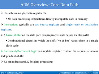
 Data items are placed in register file
 No data processing instructions directly manipulate data in memory
 Instructions typically use two source registers and single result or destination
registers.
 A barrel shifter on the data path can preprocess data before it enters ALU
 Combinational circuit in which the shift (No of bits) takes place in a single
clock cycle
 Increment/Decrement logic can update register content for sequential access
independent of ALU
 32-bit address and 32-bit data processing
75
ARM Overview: Core Data Path
Dr. V. Sathiesh Kumar Department of Electronics, MIT, India
76
Basic ARM Organization
Dr. V. Sathiesh Kumar Department of Electronics, MIT, India
 The set of registers available for use by programs is called the
programming model or programmer model. The CPU has many other
registers that are used for internal operations and are unavailable to
programmers
 General purpose registers (GPR) hold either data or address. All
registers are of 32 bits. In User mode, 16 data registers and 2 status
registers are visible
 Data registers: r0 to r15
 r13: Stack Pointer
 r14: Link Register (Where return address is put whenever a subroutine is
called)
 r15: Program counter 77
Registers
Dr. V. Sathiesh Kumar Department of Electronics, MIT, India
 Depending upon context, register r13 and r14 can also be used as
GPR
 Any instruction which use r0 can as well be used with any other
GPR (r1-r13)
 In addition, there are two status registers
 CPSR: Current Program Status Register
 SPSR: Saved Program Status Register
 Register r15 (Program counter)
 All instructions are 32 bit wide and word aligned
 PC value is stored in bits [31:2] with bits [1:0] undefined
78
Registers- Continued
Dr. V. Sathiesh Kumar Department of Electronics, MIT, India
79
CPSR
Dr. V. Sathiesh Kumar Department of Electronics, MIT, India
 Register file contains in all 37 registers
 20 registers are hidden from program at different times. These registers are
called banked registers
 Banked registers are available only when the processor is in a
particular mode
 Processor modes (other than System mode) have a set of associated banked
registers that are a subset of 16 registers
 Maps one to one onto a User mode register
80
Banked Registers
Dr. V. Sathiesh Kumar Department of Electronics, MIT, India
81
Registers Banking-Currently visible in particular
mode
Dr. V. Sathiesh Kumar Department of Electronics, MIT, India
 Processor modes determine
 which registers are active, and
 access rights to CPSR register itself
 Each processor mode is either,
 Privileged: Full read-write access to the CPSR
 Non-Privileged: Only read access to the control field of CPSR but read-write
access to the condition flags
 ARM has seven modes
 Privileged: Abort, Fast interrupt request, Interrupt request, Supervisor,
System and Undefined
 Non-Privileged: User (Programs and applications) 82
Processor Modes
Dr. V. Sathiesh Kumar Department of Electronics, MIT, India
 Abort: When there is a failed attempt to access memory
 Fast interrupt request (FIQ) and Interrupt request (IR):
Correspond to interrupt levels available on ARM
 Supervisor mode: State after reset and generally the mode in
which OS Kernel executes
 System mode: Special version of user mode that allows full read-
write access of CPSR
 Undefined: When processor encounters an undefined instructions
83
Privileged Processor Modes
Dr. V. Sathiesh Kumar Department of Electronics, MIT, India
 Each Privileged mode (except System mode) has associated with it
a save program status register or SPSR
 This SPSR is used to save the state of CPSR when the Privileged
mode is entered in order that the user state can be fully restored
when the user process is resumed
84
SPSR
Dr. V. Sathiesh Kumar Department of Electronics, MIT, India
 Mode changes by writing directly to CPSR or by hardware when
the processor responds to exception or interrupt
 To return to User mode a special return instruction is used that
instructs the core to restore the original CPSR and banked registers
85
Mode Changing
Dr. V. Sathiesh Kumar Department of Electronics, MIT, India
86
Register Organization in different modes
Dr. V. Sathiesh Kumar Department of Electronics, MIT, India
 Instructions process data held in registers and access memory
with load and store instructions.
 Classes of instructions:
 Data processing
 Branch instructions
 Load-Store instructions
 Software interrupt instructions
 Program status register instructions
87
ARM Instruction set
Dr. V. Sathiesh Kumar Department of Electronics, MIT, India
 Three address data processing instructions (two operands and
destination)
 Condition execution of every instructions
 Load and store multiple registers
 Shift, ALU operation in a single instruction
 Open instruction set extension through the co-processor
instruction
88
ARM Instruction set-Features
Dr. V. Sathiesh Kumar Department of Electronics, MIT, India
 Word is 32-bit long
 Word can be divided into four 8-bit bytes
 ARM addresses can be 32-bit long
 Address refer to a byte
 Address 4 starts at byte 4
 Can be configured at power-up as either little or big-endian mode
89
ARM Data types
Dr. V. Sathiesh Kumar Department of Electronics, MIT, India
 Manipulate data within registers
 MOVE instruction
 Arithmetic instruction includes Multiply instruction
 Logical instruction
 Comparison instruction
 Suffix S on data processing instructions updates flags in CPSR
 Operands are 32-bit wide (registers or specified as literals)
 Second operand sent to ALU via a barrel shifter
 32-bit result placed in register; long multiply instructions
produces 64-bit result
90
Data Processing
Dr. V. Sathiesh Kumar Department of Electronics, MIT, India
 MOV Rd, N (Eg: MOV r7, r5)
Rd- Destination register
N- can be an immediate value or source register
 MVN Rd, N (Move into Rd not of the 32-bit value from
source)
91
MOVE Instruction
Dr. V. Sathiesh Kumar Department of Electronics, MIT, India
92
Using Barrel Shifter
Dr. V. Sathiesh Kumar Department of Electronics, MIT, India
 Enables shifting 32-bit operand in one of the source registers left
or right by a specific number of positions within the cycle time of
instructions
 Basic barrel shifter operations
 Shift left, Shift right, Rotate right
 Facilitates fast multiply, division and increases code density
 Eg: MOV r7, r5, LSL #2 (Multiplies content of r5 by 4 and puts
the result in r7)
LSL: Logical Shift Left
93
Using Barrel Shifter
Dr. V. Sathiesh Kumar Department of Electronics, MIT, India
 Implements 32 bits addition and subtraction.
3 operand form
Eg., SUB r0, r1, r2
Subtract value stored in r2 from that of r1 and store in r0.
Eg., SUBS r1, r1, #1
Subtract 1 from r1 and store result in r1 and update z and c flags.
94
Arithmetic Instructions
Dr. V. Sathiesh Kumar Department of Electronics, MIT, India
 Use of Barrel shifter with arithmetic and logical instructions
increases the set of possible available operations.
Eg., ADD r 0, r1, r1, LSL #1
Register r1 is shifted to the left by 1, then it is added with r1 and the
result (3 times r1) is stored in r0.
95
With Barrel Shifter
Dr. V. Sathiesh Kumar Department of Electronics, MIT, India
 Multiply contents of a pair of registers.
Long multiply generates 64 bit result.
Eg., MUL r0, r1 , r2 (32 bit result) r0=r1*r2
Contents of r1 and r2 multiplied and put in r0.
Eg., UMULL r0 , r1 , r2, r3 (64 bit result) [r0, r1]=r2*r3
Unsigned long multiply with result stored in r0 and r1.
No. of cycles taken for execution of multiply instruction depends
upon processor implementation.
96
Multiply Instructions
Dr. V. Sathiesh Kumar Department of Electronics, MIT, India
 Result of multiplication can be accumulated with contents of
another register.
Eg., MLA Rd , Rm , Rs , Rn (32 bit result) [Convolution Operation]
Rd = (Rm* Rs ) + Rs
Eg., UMLAL Rdlo , Rdhi , Rm , Rn (64 bit result)
[Rdhi , Rdlo ]= [Rdhi , Rdlo ]+ (Rm* Rn)
97
Multiply and Accumulate
Dr. V. Sathiesh Kumar Department of Electronics, MIT, India
 Bit wise logical operations on the two source registers.
AND, OR, Ex-OR, bit clear
Eg., BIC r0,r1,r2
r2 contains a binary pattern where every binary 1 in r2 clears a
corresponding bit location in register r1.
Useful in manipulating status of flags and interrupt masks.
98
Logical Instructions
Dr. V. Sathiesh Kumar Department of Electronics, MIT, India
 Enables comparison of 32 bit values.
updates CPSR flags but do not affect other registers.
Eg., CMP r0 , r9
Flags set as a result of r0- r9.
Eg., TEQ r0 , r9
Flags set as a result of r0 Ex-OR r9.
Eg., TST r0, r9
Flags set as a result of r0 AND r9.
99
Compare Instructions
Dr. V. Sathiesh Kumar Department of Electronics, MIT, India
 Transfer data between memory and process registers.
 Single Register Transfer
Data types supported are signed and unsigned words (32 bits), half words,
bytes.
Multiple Register Transfer
Transfer multiple registers between memory and the processor in a single
instruction.
Swap
Swaps content of a memory location with the content of a register.
100
Load-Store Instructions
Dr. V. Sathiesh Kumar Department of Electronics, MIT, India
 Load and store data on a boundary alignment.
 LDR , LDRH , LDRB (Load- Word, Half word, Byte)
 STR , STRH , STRB (Store – Word, Half word, Byte)
 Support different addressing modes
 Register indirect: LDR r0, [r1]
 Immediate: LDR r0, [r1, #4] (12-bit offset added to the base register)
 Register operation: LDR r0, [r1,-r2] (Address calculated using base
register and another register)
 Scaled (Address is calculated using the base address register
and a barrel shifter operation)
 Pre & Post indexing 101
Single Transfer Instructions
Dr. V. Sathiesh Kumar Department of Electronics, MIT, India
 Pre-index with write back: LDR r0,[r1, #4]! (Updates the
address base register with new address)
 Post-index: LDR r0, [r1], #4 (Updates the address register
after address is used)
 Eg: Pre-indexing with write back: LDR r0, [r1, #4]!
Before instruction execution After instruction execution
r0=0x00000000, r1=0x00009000 r0=0x02020202, r1=0x00009004
Mem 32[0x00009000]=0x01010101
Mem 32[0x00009004]=0x02020202
102
Single Transfer Instructions-Pre & Post Indexing
Dr. V. Sathiesh Kumar Department of Electronics, MIT, India
 Load-Store multiple instructions transfers multiple register
contents between memory and the processor in a single instruction
 More efficient- For moving blocks of memory and saving and
restoring context and stack
 These instructions can increase interrupt latency (Usually
instruction executions are not interrupted by ARM)
103
Multiple Register Transfer Instructions
Dr. V. Sathiesh Kumar Department of Electronics, MIT, India
 Any subset of current bank of registers can be transferred to
memory or fetched from memory
 Eg: LDM SDM
 The base register Rn determines source or destination address
104
Multiple Byte Load-Store Instructions
Dr. V. Sathiesh Kumar Department of Electronics, MIT, India
 LDMIA/IB/DA/DB Ex: LDMIA Rn!, {r1-r3}
 STMIA/IB/DA/DB
N-register content N=3 (r1 to r3)
105
Addressing Modes
Start Address End Address Rn!
IA Increment After Rn Rn+4*N-4 Rn+4*N
IB Increment Before Rn+4 Rn+4*N Rn+4*N
DA Decrement after Rn-4*N+4 Rn Rn-4*N
DB Decrement before Rn-4*N Rn-4 Rn-4*N
Dr. V. Sathiesh Kumar Department of Electronics, MIT, India
 A stack is implemented as a linear data structure which grows up
(ascending) or down (descending)
 Stack pointer holds the address of the current top of the stack
106
Stack Processing
Dr. V. Sathiesh Kumar Department of Electronics, MIT, India
 ARM multiple register transfer instructions support
 Full ascending: grows up, SP points to the highest address containing a valid
item
 Empty ascending: grows up, SP points to the first empty location above stack
 Full descending: grows down, SP points to the lowest address containing a
valid data
 Empty descending: grows down, SP points to the first location below the
stack
107
Modes of Stack Operation
Dr. V. Sathiesh Kumar Department of Electronics, MIT, India
 Full ascending
LDMFA: translates to LDMDA (POP)
STMFA: translates to STMIB (PUSH)
SP points to the last item in stack
 Empty descending
LDMED: translates to LDMIB (POP)
STMED: translates to STMIA (PUSH)
SP points to first unused location
108
Some Stack Instructions
Dr. V. Sathiesh Kumar Department of Electronics, MIT, India
 Special case of load-store instruction
SWP: Swap a word between memory and register
SWPB: Swap a byte between memory and register
 Useful for implementing synchronization primitives likes
semaphores
109
Swap Instruction
Dr. V. Sathiesh Kumar Department of Electronics, MIT, India
 Branch instructions
 Conditional branches
 Conditional execution
 Branch and Link instructions
 Subroutine return instructions
110
Control flow Instructions
Dr. V. Sathiesh Kumar Department of Electronics, MIT, India
 Branch instruction: B label Ex: B forward
Address label is stored in the instruction as a signed PC-relative offset
 Conditional branch: B <Cond> label Ex: BNE loop
Branch has a condition associated with it and executed if condition codes have
the current value Ex: Block memory copy
loop LDMIA r9!, {r0-r7}
STMIA r10!, {r0-r7}
CMP r9, r11
BNE loop
r9 points to source of data, r10 points to start of destination data, r11 points to end
of the source 111
Control flow-Branch Instructions
Dr. V. Sathiesh Kumar Department of Electronics, MIT, India
 An unusual feature of ARM instruction set is that conditional
execution applies not only to branches but to all arm instructions
Ex: ADDEQ r0,r1,r2
Instruction will only be executed when the zero flag is set to 1
 Advantages:
 Reduces the number of branches
 Reduces the number of pipeline flushes
 Improves performance of the codes
 Increases code density
 Whenever the conditional sequence is 3 instructions or fewer (Smaller and
faster) to exploit conditional execution than to use a branch 112
Control flow-Conditional Execution
Dr. V. Sathiesh Kumar Department of Electronics, MIT, India
113
Control flow-Conditional Execution
Dr. V. Sathiesh Kumar Department of Electronics, MIT, India
 Perform a branch, save the return address following the branch in
the link register (r14)
Ex: BL Subroutine
 For nested subroutines, push r14 and some work registers
required to be saved onto stack in memory
Ex: BL Sub1
STMFD r13!, (r0-r2, r14)
BL Sub2
114
Branch and Link Instruction
Dr. V. Sathiesh Kumar Department of Electronics, MIT, India
 No specific instruction
Ex: Sub …
MOV PC, r14
Ex: When return address has been pushed to stack
Sub2 …
LDMFD r13!, (r0-r2, PC)
Register transfer cannot be interrupted
115
Subroutine Return Instruction
Dr. V. Sathiesh Kumar Department of Electronics, MIT, India
 A SWI causes a software interrupt exception, which provides a
mechanism for applications to OS routines
 Instruction: SWI {<Cond>} SWI_Number
 When a processor executes an SWI instruction, it sets the program
counter PC to the offset 0x8 in the vector table
 Instruction also forces the processor mode to SVC, which allows an
operating system routine to execute
 Switching of mode is possible
 SWI is typically executed in User mode
116
Software Interrupt Instruction (SWI)
Dr. V. Sathiesh Kumar Department of Electronics, MIT, India
 Instruction forces processor mode to supervisor mode (SVC)- this
allows an OS routine to be executed in privileged mode
 Each SWI has an associated SWI number which is used to
represent a particular function call or feature
 Parameter passing- through registers; Return value is also passed
using registers
117
Software Interrupt Instruction (SWI)- Continued
Dr. V. Sathiesh Kumar Department of Electronics, MIT, India
Ex: PRE: CPSR=nzcvqift USER (i-interrupt, t-thumb)
PC=0x00008000
lr=0x003fffff Link register
r0=0x12
Instruction: 0x00008000 SWI 0x123456
POST: CPSR=nzcvqift_SVC
SPSR=nzcvqift_USER
PC= 0x00008004
lr= 0x00008004 (lr=r14_SVC)
r0= 0x12
118
Software Interrupt Instruction (SWI)- Continued
Dr. V. Sathiesh Kumar Department of Electronics, MIT, India
 Two instructions to control PSR directly
 MRS- transfers contents of either CPSR or SPSR into a register
 MSR- transfers contents of registers to CPSR or SPSR
Ex: Enabling IRQ interrupt
PRE: CPSR=nzcvqift_SVC (i is not set)
MRS r1, CPSR
BIC r1, r1, # 0x80
MSR CPSR, r1
POST: CPSR=nzcvqift_SVC (i is set)
119
Program Status Register Instructions
Dr. V. Sathiesh Kumar Department of Electronics, MIT, India
 Used to extend the instruction set
 Used by cores with a co-processor
 Co-processor specific operations Ex: Memory management unit
 Syntax: Co-processor data processing
CDP {<Cond>} Cp, Opcode1, Cd, Cn, Cm, {Opcode2}
Cp- Co-processor number between p0 to p15
Opcode field describes co-processor operation
Cd, Cn, Cm- Co-processor registers
 Also Co-processor register transfer and memory transfer
instructions
120
Co-processor Instructions
Dr. V. Sathiesh Kumar Department of Electronics, MIT, India
 Thumb encodes a subset of the 32-bit instruction set into a 16-bit
subspace
 Thumb has higher performance than ARM on a processor with a
16-bit data bus
 Thumb has higher code density
 For memory constrained embedded system
 Only low registers r0 to r7 is fully accessible
 Higher registers are accessible with MOV, ADD, CMP instructions
 Barrel shift operations are separate instructions
121
Thumb Instructions
Dr. V. Sathiesh Kumar Department of Electronics, MIT, India
Ex: Code density
ARM divide Thumb divide
MOV r3, #0 MOV r3, #0
loop loop
SUBS r0, r0, r1 ADD r3, #1
ADDGE r3,r3, #1 SUB r0,r1
BGE loop BGE loop
ADD r2, r0,r1 SUB r3, #1
ADD r2, r0, r1
5 Instructions x 4 Bytes= 20 Bytes 6 Instructions x 2 Byte= 12 Bytes
122
Thumb Instructions- Continued
Dr. V. Sathiesh Kumar Department of Electronics, MIT, India
 To call a thumb routine from an ARM routine, the core has to change state
(Changing T bit in CPSR)
 BX and BLX instruction can be used for the switch
Ex: BX r0; BLX r0
Enters thumb state if bit 0 of the address in Rn is set to binary 1; otherwise it
enters ARM state
123
ARM-Thumb Interworking
Dr. V. Sathiesh Kumar Department of Electronics, MIT, India
 Thumb instruction decoder is placed in pipeline
 Change in thumb mode happens by changing the state of multiplexer A1
 A1 selects 16-bit data
124
Thumb (T) Architecture
Dr. V. Sathiesh Kumar Department of Electronics, MIT, India
 Extensions to facilitate signal processing operations
 Supports
 Signed multiply accumulate instructions
 Saturation arithmetic
 Creates flexibility and efficiency when manipulating 16-bit values for
applications such as 16-bit digital audio processing
125
ARM V5E Extensions
Dr. V. Sathiesh Kumar Department of Electronics, MIT, India
 Normal ARM instructions wrap around when there is an overflow
of an integer value
 Using ARM V5E instructions, you can saturate the result
 Once the highest number is exceeded the result remains at the maximum
value
 Minimum value does not change an underflow
Ex: Instructions: QADD, QSUB
126
Saturation Arithmetic
Dr. V. Sathiesh Kumar Department of Electronics, MIT, India
 Definition of an embedded system
History of embedded systems
Embedded system design process
Formalism of embedded system design
Model train controller
ARM processor fundamentals
ARM instruction set and programming
127
Summary

More Related Content

What's hot

Hardware Software Codesign
Hardware Software CodesignHardware Software Codesign
Hardware Software Codesign
destruck
 
8051 Microcontroller Notes
8051 Microcontroller Notes8051 Microcontroller Notes
8051 Microcontroller Notes
Dr.YNM
 

What's hot (20)

ARM - Advance RISC Machine
ARM - Advance RISC MachineARM - Advance RISC Machine
ARM - Advance RISC Machine
 
Arm processor
Arm processorArm processor
Arm processor
 
LPC 2148 ARM MICROCONTROLLER
LPC 2148 ARM MICROCONTROLLERLPC 2148 ARM MICROCONTROLLER
LPC 2148 ARM MICROCONTROLLER
 
Module 2 ARM CORTEX M3 Instruction Set and Programming
Module 2 ARM CORTEX M3 Instruction Set and ProgrammingModule 2 ARM CORTEX M3 Instruction Set and Programming
Module 2 ARM CORTEX M3 Instruction Set and Programming
 
ARM7-ARCHITECTURE
ARM7-ARCHITECTURE ARM7-ARCHITECTURE
ARM7-ARCHITECTURE
 
Introduction to arm architecture
Introduction to arm architectureIntroduction to arm architecture
Introduction to arm architecture
 
ARM Architecture
ARM ArchitectureARM Architecture
ARM Architecture
 
Unit II Arm 7 Introduction
Unit II Arm 7 IntroductionUnit II Arm 7 Introduction
Unit II Arm 7 Introduction
 
8085 microprocessor ramesh gaonkar
8085 microprocessor   ramesh gaonkar8085 microprocessor   ramesh gaonkar
8085 microprocessor ramesh gaonkar
 
Arm cortex-m4 programmer model
Arm cortex-m4 programmer modelArm cortex-m4 programmer model
Arm cortex-m4 programmer model
 
Embedded System Programming on ARM Cortex M3 and M4 Course
Embedded System Programming on ARM Cortex M3 and M4 CourseEmbedded System Programming on ARM Cortex M3 and M4 Course
Embedded System Programming on ARM Cortex M3 and M4 Course
 
Embedded Systems (18EC62) - ARM Cortex-M3 Instruction Set and Programming (Mo...
Embedded Systems (18EC62) - ARM Cortex-M3 Instruction Set and Programming (Mo...Embedded Systems (18EC62) - ARM Cortex-M3 Instruction Set and Programming (Mo...
Embedded Systems (18EC62) - ARM Cortex-M3 Instruction Set and Programming (Mo...
 
Unit vi (2)
Unit vi (2)Unit vi (2)
Unit vi (2)
 
Hardware Software Codesign
Hardware Software CodesignHardware Software Codesign
Hardware Software Codesign
 
I2C Protocol
I2C ProtocolI2C Protocol
I2C Protocol
 
8086 microprocessor-architecture
8086 microprocessor-architecture8086 microprocessor-architecture
8086 microprocessor-architecture
 
PIC 16F877A by PARTHIBAN. S.
PIC 16F877A   by PARTHIBAN. S.PIC 16F877A   by PARTHIBAN. S.
PIC 16F877A by PARTHIBAN. S.
 
ARM architcture
ARM architcture ARM architcture
ARM architcture
 
8051 Microcontroller Notes
8051 Microcontroller Notes8051 Microcontroller Notes
8051 Microcontroller Notes
 
ARM Micro-controller
ARM Micro-controllerARM Micro-controller
ARM Micro-controller
 

Similar to Unit 1 Introduction to Embedded computing and ARM processor

Embedded System
Embedded SystemEmbedded System
Embedded System
surendar
 

Similar to Unit 1 Introduction to Embedded computing and ARM processor (20)

UNIT I.pptx
UNIT I.pptxUNIT I.pptx
UNIT I.pptx
 
UNIT I_Introduction.pptx
UNIT I_Introduction.pptxUNIT I_Introduction.pptx
UNIT I_Introduction.pptx
 
ERTS_Unit 1_PPT.pdf
ERTS_Unit 1_PPT.pdfERTS_Unit 1_PPT.pdf
ERTS_Unit 1_PPT.pdf
 
EFFECTIVE EMBEDDED SYSTEMS SOFTWARE DESIGN METHODOLOGIES
EFFECTIVE EMBEDDED SYSTEMS SOFTWARE DESIGN METHODOLOGIESEFFECTIVE EMBEDDED SYSTEMS SOFTWARE DESIGN METHODOLOGIES
EFFECTIVE EMBEDDED SYSTEMS SOFTWARE DESIGN METHODOLOGIES
 
UNIT 1.docx
UNIT 1.docxUNIT 1.docx
UNIT 1.docx
 
Module-1 Embedded computing.pdf
Module-1 Embedded computing.pdfModule-1 Embedded computing.pdf
Module-1 Embedded computing.pdf
 
btech embedded systems ppt ES UNIT-1.pptx
btech embedded systems ppt ES UNIT-1.pptxbtech embedded systems ppt ES UNIT-1.pptx
btech embedded systems ppt ES UNIT-1.pptx
 
lec 1Embedded System Design ppt.pptx
lec 1Embedded System Design ppt.pptxlec 1Embedded System Design ppt.pptx
lec 1Embedded System Design ppt.pptx
 
Embedded systems- nanocdac
Embedded systems- nanocdacEmbedded systems- nanocdac
Embedded systems- nanocdac
 
UNIT 1.pptx
UNIT 1.pptxUNIT 1.pptx
UNIT 1.pptx
 
1. An Introduction to Embed Systems_DRKG.pptx
1. An Introduction to Embed Systems_DRKG.pptx1. An Introduction to Embed Systems_DRKG.pptx
1. An Introduction to Embed Systems_DRKG.pptx
 
Introduction to Embedded System I: Chapter 2 (5th portion)
Introduction to Embedded System I: Chapter 2 (5th portion)Introduction to Embedded System I: Chapter 2 (5th portion)
Introduction to Embedded System I: Chapter 2 (5th portion)
 
Embedded System
Embedded SystemEmbedded System
Embedded System
 
ES-Basics.pdf
ES-Basics.pdfES-Basics.pdf
ES-Basics.pdf
 
Ntroduction to computer architecture and organization
Ntroduction to computer architecture and organizationNtroduction to computer architecture and organization
Ntroduction to computer architecture and organization
 
Ijetr042175
Ijetr042175Ijetr042175
Ijetr042175
 
Embedded systems
Embedded systemsEmbedded systems
Embedded systems
 
Embedded system
Embedded systemEmbedded system
Embedded system
 
Embeddedsystem
EmbeddedsystemEmbeddedsystem
Embeddedsystem
 
Introduction to Embedded Systems
Introduction to Embedded SystemsIntroduction to Embedded Systems
Introduction to Embedded Systems
 

Recently uploaded

ONLINE VEHICLE RENTAL SYSTEM PROJECT REPORT.pdf
ONLINE VEHICLE RENTAL SYSTEM PROJECT REPORT.pdfONLINE VEHICLE RENTAL SYSTEM PROJECT REPORT.pdf
ONLINE VEHICLE RENTAL SYSTEM PROJECT REPORT.pdf
Kamal Acharya
 
Laundry management system project report.pdf
Laundry management system project report.pdfLaundry management system project report.pdf
Laundry management system project report.pdf
Kamal Acharya
 
Standard Reomte Control Interface - Neometrix
Standard Reomte Control Interface - NeometrixStandard Reomte Control Interface - Neometrix
Standard Reomte Control Interface - Neometrix
Neometrix_Engineering_Pvt_Ltd
 
Online blood donation management system project.pdf
Online blood donation management system project.pdfOnline blood donation management system project.pdf
Online blood donation management system project.pdf
Kamal Acharya
 

Recently uploaded (20)

ONLINE VEHICLE RENTAL SYSTEM PROJECT REPORT.pdf
ONLINE VEHICLE RENTAL SYSTEM PROJECT REPORT.pdfONLINE VEHICLE RENTAL SYSTEM PROJECT REPORT.pdf
ONLINE VEHICLE RENTAL SYSTEM PROJECT REPORT.pdf
 
Laundry management system project report.pdf
Laundry management system project report.pdfLaundry management system project report.pdf
Laundry management system project report.pdf
 
Peek implant persentation - Copy (1).pdf
Peek implant persentation - Copy (1).pdfPeek implant persentation - Copy (1).pdf
Peek implant persentation - Copy (1).pdf
 
RESORT MANAGEMENT AND RESERVATION SYSTEM PROJECT REPORT.pdf
RESORT MANAGEMENT AND RESERVATION SYSTEM PROJECT REPORT.pdfRESORT MANAGEMENT AND RESERVATION SYSTEM PROJECT REPORT.pdf
RESORT MANAGEMENT AND RESERVATION SYSTEM PROJECT REPORT.pdf
 
Online resume builder management system project report.pdf
Online resume builder management system project report.pdfOnline resume builder management system project report.pdf
Online resume builder management system project report.pdf
 
Event Management System Vb Net Project Report.pdf
Event Management System Vb Net  Project Report.pdfEvent Management System Vb Net  Project Report.pdf
Event Management System Vb Net Project Report.pdf
 
A CASE STUDY ON ONLINE TICKET BOOKING SYSTEM PROJECT.pdf
A CASE STUDY ON ONLINE TICKET BOOKING SYSTEM PROJECT.pdfA CASE STUDY ON ONLINE TICKET BOOKING SYSTEM PROJECT.pdf
A CASE STUDY ON ONLINE TICKET BOOKING SYSTEM PROJECT.pdf
 
HYDROPOWER - Hydroelectric power generation
HYDROPOWER - Hydroelectric power generationHYDROPOWER - Hydroelectric power generation
HYDROPOWER - Hydroelectric power generation
 
Halogenation process of chemical process industries
Halogenation process of chemical process industriesHalogenation process of chemical process industries
Halogenation process of chemical process industries
 
İTÜ CAD and Reverse Engineering Workshop
İTÜ CAD and Reverse Engineering WorkshopİTÜ CAD and Reverse Engineering Workshop
İTÜ CAD and Reverse Engineering Workshop
 
fundamentals of drawing and isometric and orthographic projection
fundamentals of drawing and isometric and orthographic projectionfundamentals of drawing and isometric and orthographic projection
fundamentals of drawing and isometric and orthographic projection
 
Standard Reomte Control Interface - Neometrix
Standard Reomte Control Interface - NeometrixStandard Reomte Control Interface - Neometrix
Standard Reomte Control Interface - Neometrix
 
Online blood donation management system project.pdf
Online blood donation management system project.pdfOnline blood donation management system project.pdf
Online blood donation management system project.pdf
 
NO1 Pandit Amil Baba In Bahawalpur, Sargodha, Sialkot, Sheikhupura, Rahim Yar...
NO1 Pandit Amil Baba In Bahawalpur, Sargodha, Sialkot, Sheikhupura, Rahim Yar...NO1 Pandit Amil Baba In Bahawalpur, Sargodha, Sialkot, Sheikhupura, Rahim Yar...
NO1 Pandit Amil Baba In Bahawalpur, Sargodha, Sialkot, Sheikhupura, Rahim Yar...
 
KIT-601 Lecture Notes-UNIT-4.pdf Frequent Itemsets and Clustering
KIT-601 Lecture Notes-UNIT-4.pdf Frequent Itemsets and ClusteringKIT-601 Lecture Notes-UNIT-4.pdf Frequent Itemsets and Clustering
KIT-601 Lecture Notes-UNIT-4.pdf Frequent Itemsets and Clustering
 
Furniture showroom management system project.pdf
Furniture showroom management system project.pdfFurniture showroom management system project.pdf
Furniture showroom management system project.pdf
 
Top 13 Famous Civil Engineering Scientist
Top 13 Famous Civil Engineering ScientistTop 13 Famous Civil Engineering Scientist
Top 13 Famous Civil Engineering Scientist
 
fluid mechanics gate notes . gate all pyqs answer
fluid mechanics gate notes . gate all pyqs answerfluid mechanics gate notes . gate all pyqs answer
fluid mechanics gate notes . gate all pyqs answer
 
The Benefits and Techniques of Trenchless Pipe Repair.pdf
The Benefits and Techniques of Trenchless Pipe Repair.pdfThe Benefits and Techniques of Trenchless Pipe Repair.pdf
The Benefits and Techniques of Trenchless Pipe Repair.pdf
 
ASME IX(9) 2007 Full Version .pdf
ASME IX(9)  2007 Full Version       .pdfASME IX(9)  2007 Full Version       .pdf
ASME IX(9) 2007 Full Version .pdf
 

Unit 1 Introduction to Embedded computing and ARM processor

  • 1. EC8011- Embedded and Real-Time Systems Dr. V. Sathiesh Kumar Department of Electronics, MIT, India UNIT-I: INTRODUCTION TO EMBEDDED COMPUTING AND ARM PROCESSORS Complex systems and microprocessors – Embedded system design process – Formalism for system design– Design example: Model train controller- ARM Processor Fundamentals- Instruction Set and Programming using ARM Processor. TEXTBOOKS 1. Wayne Wolf, “Computers as Components - Principles of Embedded Computing System Design”, Morgan Kaufmann Publisher (An imprint from Elsevier), Second Edition ,2008. 2. Andrew N Sloss, Dominic Symes, Chris Wright, “ARM System Developer’s Guide- Designing and Optimizing System Software”, Elsevier/Morgan Kaufmann Publisher, 2008. www.sathieshkumar.com/tutorials 1
  • 2. Dr. V. Sathiesh Kumar Department of Electronics, MIT, India 2
  • 3. Definition of an Embedded System Dr. V. Sathiesh Kumar Department of Electronics, MIT, India  An Embedded system is a system designed to perform one or few dedicated functions often with real time computing constraints. It is embedded as a part of a complete device often including hardware (mechanical parts, electronic devices) and softwares. Processing Unit Human Interface Sensors RTOS Actuator 3
  • 4. History of Embedded Computers Dr. V. Sathiesh Kumar Department of Electronics, MIT, India  Whirlwind- First computer designed to support real-time operation at MIT, USA in early 1950. It contains over 4000 vacuum tubes. Very Large Scale Integration (VLSI) technology allowed us to embed a complete CPU on a single chip in 1970’s and termed as microprocessor.  Intel 4004- First microprocessor designed to be used as an calculator. Hp-35- First handheld calculator (Several chips are used to implement the CPU). Automobiles- Determining when spark plugs fire, controlling the fuel/air mixture and so on. A high-end automobile may have 100 microprocessors, but even inexpensive cars today use 40 microprocessors. 4
  • 5. EMBEDDED SYSTEM = HARDWARE + SOFTWARE Dr. V. Sathiesh Kumar Department of Electronics, MIT, India 5 Hardware Peripherals Processor 1. Microcontroller (C) 2. Digital signal processors (DSP) 3. FPGA core (VLSI) Processor Peripherals MEMORY, Serial Ports (SCI,SPI,CAN,USB), Parallel Port, ADC (8/12/16/24 bit), DAC, PWM etc.. +3 to 5 V Supply Digital I/O lines SPI,I2C,SCI Memory ALU Timer ADC/DAC PWM
  • 6. Classification of Microprocessors Dr. V. Sathiesh Kumar Department of Electronics, MIT, India  A 8-bit microcontroller- designed for low-cost applications and includes on-board memory and I/O devices. Eg: Atmel- AT89C51, Microchip-PIC 16F877, Motorolla- 68HC11  A 16-bit microcontroller- more sophisticated applications that may require either longer word lengths or off-chip I/O and memory. Eg: DsPIC, PIC24 Series  A 32-bit RISC microprocessor- offers very high performance for computation-intensive applications. Eg: PIC 32 Series, ARM Processors (Series 7 and 9) 6
  • 7. Advantage of Programmable CPU to Hardwired Unit Dr. V. Sathiesh Kumar Department of Electronics, MIT, India  It is easier to design and debug.  It allows the possibility of upgrades and using the CPU for other purposes. Why use Microprocessors?  Microprocessors are a very efficient way to implement digital systems.  Microprocessors make it easier to design families of products. Faster implementation of your application than designing your own custom logic (Overhead in fetching, decoding and executing the program is overcome by a single clock cycle instruction execution and pipelining strategy).  Many different algorithms can be implemented by simply changing the program it executes.  Low power consumption. 7
  • 8. Functionality of Embedded Computing Systems Dr. V. Sathiesh Kumar Department of Electronics, MIT, India  Complex algorithms: Operations performed by the microprocessor may be very sophisticated. Eg: In automobiles, microprocessor needs to perform complicated filtering functions to optimize the performance of the car while minimizing pollution and fuel utilization.  User interface: Multiple menus , displays, input terminals (Keyboard, Touch screen). Eg: Moving maps in Global Positioning System (GPS) navigation.  Real time: Embedded computing operations must be performed to meet deadlines. Failure to meet a deadline is unsafe and can even endanger lives (Eg: Controlling brakes on wheel)  Multirate: Embedded computing systems needs to support different operational speeds (The audio and video portions of a multimedia stream run at very different rates, but they must remain closely synchronized) 8
  • 9. Functionality of Embedded Computing Systems Dr. V. Sathiesh Kumar Department of Electronics, MIT, India  Manufacturing cost: Determined by many factors such as type of microprocessor used, the amount of memory required and the type of I/O devices.  Power and energy: Power consumption directly affects the cost of the hardware. Energy consumption affects battery life. 9
  • 10. Challenges in Embedded Computing System Design Dr. V. Sathiesh Kumar Department of Electronics, MIT, India  How much hardware do we need? Too little hardware and the system fails to meet its deadlines, too much hardware and it becomes too expensive.  How do we meet deadlines? Speed up the hardware-makes system more expensive Increasing the CPU clock rate may not make enough difference to execution time, since the program speed may be limited by the memory system.  How do we minimize power consumption? Excessive power consumption can increase heat dissipation. Careful design is required to slow down the noncritical parts of the machine for power consumption while still meeting necessary performance goals. 10
  • 11. Challenges in Embedded Computing System Design Dr. V. Sathiesh Kumar Department of Electronics, MIT, India  How do we design for upgradability? Hardware platform may be used for different versions of a product, with few or no changes. However we want to be able to add features by changing software.  Does it really work? Reliability is especially important in some applications, such as safety-critical systems. Complex testing. Limited observability and controllability- it is more difficult to see what is going on inside the system (watch the values of electrical signals if the embedded system does not come with keyboard and screen). Restricted development environments-debugging and programming the embedded system is carried out using PC. 11
  • 12. Performance in Embedded Computing Dr. V. Sathiesh Kumar Department of Electronics, MIT, India  The program must meet its deadline (is the time at which a computation must be finished).  Heart of embedded computing is real-time computing.  A large, complex program running on a sophisticated microprocessor, may or may not meet the deadline.  Analyze the system at several different levels of abstraction. These levels include, CPU (pipelined processor with cache). Platform (includes the bus and I/O devices). Program (Programs are very large and the CPU sees only a small window of the program at a time). Multitasking (Task interaction with each other). Multiprocessor (Interaction between the processors adds yet more complexity to the analysis of overall system performance).12
  • 13. Embedded System Design Process-Design Methodology Dr. V. Sathiesh Kumar Department of Electronics, MIT, India 13
  • 14. Embedded System Design Process-Design Methodology Dr. V. Sathiesh Kumar Department of Electronics, MIT, India  In bottom-up design approach, we start with components to build a system. Decisions at one stage of design are based upon estimates of what will happen later. At each step in the design, • We must analyze the design (How we can meet the specifications). • We must refine the design to add detail. • We must verify the design to ensure that it still meets all system goals, such as cost, speed and so on. 14
  • 15. Embedded System Design Process-Design Methodology Dr. V. Sathiesh Kumar Department of Electronics, MIT, India  Requirement: What is needed? Or what we are designing. Requirements may be functional or non-functional (performance, cost- Manufacturing cost (components and assembly) and nonrecurring engineering (NRE) costs (personnel and other costs of designing the system), Physical size and weight and power consumption-Battery powered systems).  Specification: More detailed description of what we want. It does not describe about, how the system is built (contains enough information to begin designing the system architecture).  Architecture: System’s internals begin to take shape.  Components: Component identification with respect to the architecture built.  System integration: Connecting the components to build a hardware and an appropriate software needs to be integrated with the hardware. 15
  • 16. Embedded System Design Process-Design Methodology-Requirement Dr. V. Sathiesh Kumar Department of Electronics, MIT, India  Requirement: What is needed? Or what we are designing. Requirements may be functional or non-functional (performance, cost- Manufacturing cost (components and assembly) and nonrecurring engineering (NRE) costs (personnel and other costs of designing the system), Physical size and weight and power consumption-Battery powered systems).  Sample requirement form : • Name (crystallize the purpose of the machine) •Purpose (one or two line description of what the system is supposed to do) • Inputs and Outputs (Type of data-Analog or Digital or Mechanical inputs, Data characteristics- Periodic or occasional arriving of data and data size, Types of I/O devices-Buttons or ADC or video displays) • Functions (more detailed description of what the system does) • Performance (computations must be performed within a time frame) • Manufacturing cost (to have an idea of the eventual cost range) 16
  • 17. Embedded System Design Process-Design Methodology-Requirement Dr. V. Sathiesh Kumar Department of Electronics, MIT, India  Sample requirement form (continued): • Power (estimate the power consumed by the device, System will be battery powered or plugged into the wall, Battery powered machines must be much more careful about how they spend energy) • Physical size and weight (give some indication of the physical size of the system to help guide certain architectural decisions)  Example 1: Requirement analysis of a GPS moving map, a satellite based navigation system 17
  • 18. Embedded System Design Process-Design Methodology-Requirement Dr. V. Sathiesh Kumar Department of Electronics, MIT, India  Functionality: for highway driving and similar uses, not nautical or aviation uses that require more specialized databases and functions. The system should show major roads and other landmarks available in standard topographic databases.  User Interface: The screen should have at least 400x600 pixel resolution. The device should be controlled by no more than three buttons. A menu system should pop up on the screen when buttons are pressed to allow the user to make selections to control the system.  Performance: The map should scroll smoothly. Upon power-up, a display should take no more than one second to appear, and the system should be able to verify its position and display the current map within 15 s. 18
  • 19. Embedded System Design Process-Design Methodology-Requirement Dr. V. Sathiesh Kumar Department of Electronics, MIT, India  Cost: The selling cost (street price) of the unit should be no more than $100.  Physical size and weight: The device should fit comfortably in the palm of the hand.  Power consumption: The device should run for at least eight hours on four AA batteries. 19
  • 20. Dr. V. Sathiesh Kumar Department of Electronics, MIT, India  more specific (contracts between the customer and the architects)  no faulty assumptions  it should be understandable enough so that someone can verify that it meets system requirements and overall expectations of the customer. Designers can run into several different types of problems caused by unclear specifications like implementing the wrong functionality. 20 Embedded System Design Process-Design Methodology-Specification
  • 21. Dr. V. Sathiesh Kumar Department of Electronics, MIT, India  A specification of the GPS system would include several components: Data received from the GPS satellite constellation  map data  User interface  Operations that must be performed to satisfy customer requests  Background actions required to keep the system running, such as operating the GPS receiver 21 Embedded System Design Process-Design Methodology-Specification
  • 22. Dr. V. Sathiesh Kumar Department of Electronics, MIT, India  Describing how the system implements those functions (specifications) is the purpose of the architecture  The architecture is a plan for the overall structure of the system  Architectural descriptions must be designed to satisfy both functional and non functional (cost, speed, power) requirements.  Block diagram of the GPS moving map 22 Embedded System Design Process-Design Methodology-Architecture Design
  • 23. Dr. V. Sathiesh Kumar Department of Electronics, MIT, India 23 Embedded System Design Process-Design Methodology-Architecture Design
  • 24. Dr. V. Sathiesh Kumar Department of Electronics, MIT, India  In hardware block diagram, a CPU is surrounded by memory and I/O devices  Two memories: a frame buffer for the pixels to be displayed and a separate program/data memory for general use by the CPU  In software block diagram, a timer has been added to control when we read the buttons on the user interface and render data onto the screen. 24 Embedded System Design Process-Design Methodology-Architecture Design
  • 25. Dr. V. Sathiesh Kumar Department of Electronics, MIT, India  The component design effort builds those components in conformance to the architecture and specification.  The components will in general include both hardware-FPGAs, boards and so on- and software modules.  We can make use of standard components and software modules (Eg: Standard topographic database- not only is the data in a predefined format, but it is highly compresses to save storage)-saves us design time.  We will also have to design some components (Eg: PCB design), custom programming.  We also must ensure that the system runs properly in real time and does not occupy a large memory space than is allowed.  The power consumption of moving map software is very important (Memory accesses are a major source of power consumption, memory transactions must be carefully planned to avoid reading the same data several times). 25 ESD Process-Design Methodology-Designing Hardware and Software Components
  • 26. Dr. V. Sathiesh Kumar Department of Electronics, MIT, India  Interconnect the components to build a system.  Identify the bugs and rectify it.  Building up the system in phases and running properly chosen tests, we can often find bugs more easily. Careful attention to inserting appropriate debugging facilities during design can help ease system integration problems, but the nature of embedded computing means that this phase will always be a challenge. 26 ESD Process-Design Methodology-System Integration
  • 27. Dr. V. Sathiesh Kumar Department of Electronics, MIT, India  Unified Modeling Language (UML) is a visual language to represent design tasks such as creating requirements, specifications, architecting the system, designing code and designing tests.  UML is useful because it encourages design by successive refinement and progressively adding detail to the design, rather than rethinking the design at each new level of abstraction.  UML is an object-oriented modeling language. Two concepts of importance are, • encourages the design to be described as a number of interacting objects, rather than a few large monolithic blocks of code. • at least some of those objects will correspond to real pieces of software or hardware in the system.  UML is so rich, there are many graphical elements in a UML diagram. 27 Formalisms for System Design
  • 28. Dr. V. Sathiesh Kumar Department of Electronics, MIT, India  Object-oriented (OO) specification can be seen in two complementary ways, • allows a system to be described in a way that closely models real-world objects and their interactions. • provides a basic set of primitives that can be used to describe systems with particular attributes, irrespective of the relationships of those systems components to real world objects.  UML can be of two categories, • Structural Description • Behavioral Description 28 Formalisms for System Design
  • 29. Dr. V. Sathiesh Kumar Department of Electronics, MIT, India  Basic components of the system.  An object includes a set of attributes that define its internal state.  UML for describing a display (CRT screen)  Note: folded corner page icon- It does not correspond to an object in the system and only serves a comment.  The object is identified in two ways: It has a unique name, and it is a member of a class 29 Structural Description
  • 30. Dr. V. Sathiesh Kumar Department of Electronics, MIT, India  A class is a form of type definition-all objects derived from the same class have the same characteristics, although their attributes may have different values. A class defines the attributes than an object may have. It also defines the operations that determine how the object interacts with the rest of the world. 30 Structural Description
  • 31. Dr. V. Sathiesh Kumar Department of Electronics, MIT, India  A class defines both the interface for a particular type of object and that objects implementation.  Several types of relationships that can exist between objects and classes,  Association occurs between objects that communicate with each other but have no ownership relationship between them.  Aggregation describes a complex object made of smaller objects.  Composition is a type of aggregation in which the owner does not allow access to the component objects.  Generalization allows us to define one class in terms of another.  UML allows to define one class in terms of another.  A derived class inherits all the attributes and operations from its base class. 31 Structural Description
  • 32. Dr. V. Sathiesh Kumar Department of Electronics, MIT, India 32 Structural Description
  • 33. Dr. V. Sathiesh Kumar Department of Electronics, MIT, India  Inheritance has two purposes,  allows us to succinctly describe one class that shares some characteristics with another class.  it captures those relationships between classes and documents.  UML also allows us to define multiple inheritance, in which a class is derived from more than one base class. 33 Structural Description
  • 34. Dr. V. Sathiesh Kumar Department of Electronics, MIT, India  A link describes a relationship between objects.  Association is to link as class is to object. 34 Structural Description
  • 35. Dr. V. Sathiesh Kumar Department of Electronics, MIT, India  One way to specify the behavior of an operation is a state machine.  State machines will not rely on the operation of a clock, as in hardware, rather, changes from one state to another are triggered by the occurrence of events.  An event may originate from outside (pressing a button) or from inside (when one routine finishes its computation and passes the result on to another routine). 35 Behavioral Description
  • 36. Dr. V. Sathiesh Kumar Department of Electronics, MIT, India  Three types of events defined by UML,  A signal is an asynchronous occurrence (<<signal>>- defined in UML).  A call event follows the model of a procedure call in a programming language.  A time-out event causes the machine to leave a state after a certain amount of time (tm(time-value)- defined in UML). The time-out is generally implemented with an external timer. 36 Behavioral Description
  • 37. Dr. V. Sathiesh Kumar Department of Electronics, MIT, India 37 Behavioral Description
  • 38. Dr. V. Sathiesh Kumar Department of Electronics, MIT, India  A sequence diagram is somewhat similar to a hardware timing diagram, although the time flows vertically in a sequence diagram, whereas time typically flows horizontally in a timing diagram.  A sequence diagram is designed to show a particular scenario or choice of events. 38 Behavioral Description
  • 39. Dr. V. Sathiesh Kumar Department of Electronics, MIT, India  The sequence shows what happens when a mouse click is on the menu region. Processing includes three objects shown at the top of the diagram. Extending below each object is its lifeline, a dashed line that shows how long the object is alive.  Focus of control in the sequence, that is, when the object is actively processing. 39 Behavioral Description
  • 40. Dr. V. Sathiesh Kumar Department of Electronics, MIT, India  The user sends messages to the train with a control box attached to the tracks.  The train receives its electrical power from the two rails of the track, the control box can send signals to the train over the tracks by modulating the power supply voltage.  The control panel send packets over the tracks to the receiver on the train.  The train includes analog electronics to sense the bits transmitted and a control system to set the train motor speed and direction based on those commands.  Each packet includes an address so that the console can control several trains on the same track; the packet also includes an error correction code (ECC) to guard against transmission errors-One way communication system. 40 Model Train Controller
  • 41. Dr. V. Sathiesh Kumar Department of Electronics, MIT, India 41 Model Train Controller
  • 42. Dr. V. Sathiesh Kumar Department of Electronics, MIT, India  The console shall be able to control up to eight trains on a single track.  The speed of each train shall be controllable by a throttle to at least 63 different levels in each direction (forward and reverse).  Inertia control is used to adjust the responsiveness of the train to commanded changes in speed. Higher inertia means that the train responds more slowly to a change in the throttle, simulating the inertia of a large train. The inertia control will provide at least different levels.  There shall be an emergency stop button.  An error detection scheme will be used to transmit messages. 42 Model Train Controller-Requirements
  • 43. Dr. V. Sathiesh Kumar Department of Electronics, MIT, India 43 Model Train Controller-Requirements
  • 44. Dr. V. Sathiesh Kumar Department of Electronics, MIT, India  Digital Command Control (DCC) standard is given in two documents, Standard S-9.1, the DCC Electrical Standard, defines how bits are encoded on the rails for transmission. (Allowable transition times for signals)  Standard S-9.2, the DCC Communication Standard, defines the packets that carry information. (PSA(sD)+E) 44 Model Train Controller-DCC
  • 45. Dr. V. Sathiesh Kumar Department of Electronics, MIT, India  Standard S-9.2, the DCC Communication Standard, defines the packets that carry information. (PSA(sD)+E)  P is the preamble (sequence of at least 10 1 bits).  S is the packet start bit (0 bit).  A is an address data byte that gives the address of the unit, with the MSB of the address transmitted first. An address is eight bits long. The addresses 00000000, 11111110 and 11111111 are reserved.  s is the data byte start bit, which, like the packet start bit, is a 0.  D is the data byte (eight bits). A data byte may contain an address, instruction, data or error correction information.  E is a packet end bit (1 bit). 45 Model Train Controller-DCC
  • 46. Dr. V. Sathiesh Kumar Department of Electronics, MIT, India A baseline packet is the minimum packet that must be accepted by all DCC implementations.  A baseline packet has three data bytes: an address data byte that gives the intended receiver of the packet, the instruction data byte provides a basic instruction and an error correction data byte is used to detect and correct transmission errors.  The instruction data byte carries several pieces of information. Bits 0-3 provide a 4-bit speed value. Bit 4 has an additional speed bit. Bit 5 gives direction, with 1 for forward and 0 for reverse. Bits 6-7 are set at 01 to indicate that this instruction provides speed and direction.  The error correction data byte is the bitwise XOR of the address and instruction data bytes.  Command unit should send packets frequently since a packet may be corrupted. Packets should be separated by at least 5 ms. 46 Model Train Controller-DCC
  • 47. Dr. V. Sathiesh Kumar Department of Electronics, MIT, India  A train control system turns commands into packets.  Two major subsystems: the command unit and the train-board component. Class diagram for the train controller messages 47 Model Train Controller-Conceptual Specification
  • 48. Dr. V. Sathiesh Kumar Department of Electronics, MIT, India  The command unit and receiver are each represented by objects; the command unit sends a sequence of packets to the trains receiver.  The notation on the arrow provides both the type of message sent and its sequence in a flow of messages; since the console sends all the messages (1..n). UML collaboration diagram for major subsystems of the train controller system 48 Model Train Controller-Conceptual Specification
  • 49. Dr. V. Sathiesh Kumar Department of Electronics, MIT, India  Console needs to perform three functions: read the state of the front panel on the command unit, format messages and transmit messages.  Train receiver also performs three functions: receive the message, interpret the message and actually control the motor.  The Console class describes the command units front panel, which contains the analog knobs and hardware to interface to the digital parts of the system.  The Formatter class includes behaviors that know how to read the panel knobs and creates a bit stream for the required message.  The Transmitter class interfaces to analog electronics to send the message along the track.  Knobs- analog knobs, buttons and levers on the control panel.  Sender- the analog electronics that send bits along the track. 49 Model Train Controller-Conceptual Specification
  • 50. Dr. V. Sathiesh Kumar Department of Electronics, MIT, India 50 Model Train Controller-Conceptual Specification
  • 51. Dr. V. Sathiesh Kumar Department of Electronics, MIT, India  The Receiver class- turns the analog signals on the track into digital form.  The Controller class- interpret the commands and figures out how to control the motor.  The Motor interface class- how to generate the analog signals required to control the motor.  Detector- detects analog signals on the track and converts them into digital form.  Pulser- turns digital commands into the analog signals required to control the motor speed.  Train set- system can handle multiple trains (1 train set can have t trains). 51 Model Train Controller-Conceptual Specification
  • 52. Dr. V. Sathiesh Kumar Department of Electronics, MIT, India  Detailed specification includes attributes and behaviors of the classes. 52 Model Train Controller-Detailed Specification
  • 53. Dr. V. Sathiesh Kumar Department of Electronics, MIT, India  The Panel has three knobs: train number (which train is currently being controlled), speed (which can be positive or negative) and inertia. It also has one button for emergency-stop.  set-knobs behavior allows the rest of the system to modify the knob settings.  The Sender and Detector classes- put out and pick up a bit.  Pulser class- control the train motor speed (Pulse width modulation). 53 Model Train Controller-Detailed Specification
  • 54. Dr. V. Sathiesh Kumar Department of Electronics, MIT, India  Panel class- behavior for each of the controls on the panel. The new-settings behavior uses the set-knobs behavior of the Knobs class to change the knobs settings whenever the train number setting is changed.  Motor-interface class- defines an attribute for speed. 54 Model Train Controller-Detailed Specification
  • 55. Dr. V. Sathiesh Kumar Department of Electronics, MIT, India 55 Model Train Controller-Detailed Specification
  • 56. Dr. V. Sathiesh Kumar Department of Electronics, MIT, India  The Transmitter provides a distinct behavior for each type of message that can be sent, it internally takes care of formatting the message.  The Receiver class provides a read-cmd behavior to read a message off the tracks. Internal variable to hold the current command. No separate behavior for an Estop message since it has no parameters.  The Formatter holds the current control settings for all of the trains. The send-command- serves as the interface to the transmitter. The operate function performs the basic actions for the object.  The Formatter repeatedly reads the panel, determines whether any settings have changed, and sends out the appropriate messages.  The panel-active behavior returns true whenever the panel’s values do not correspond to the current values. 56 Model Train Controller-Detailed Specification
  • 57. Dr. V. Sathiesh Kumar Department of Electronics, MIT, India Model Train Controller-Detailed Specification 57 Model Train Controller-Detailed Specification
  • 58. Dr. V. Sathiesh Kumar Department of Electronics, MIT, India  Sequence diagram during the panel operation. Figure shows two changes to the knob settings: first to the throttle, inertia or emergency stop; then to the train number.  The panel is called periodically by the formatter to determine if any control settings have changed.  If a setting has changed for the current train, the formatter decides to send a command, issuing a send-command behavior to cause the transmitter to send the bits.  Because the transmission is serial, it takes a noticeable amount of time for the transmitter to finish a command; in a the meantime, the formatter continues to check the panel’s control settings.  If the train number has changed, the formatter must cause the knob settings to be reset to the proper values for the new train. 58 Model Train Controller-Detailed Specification
  • 59. Dr. V. Sathiesh Kumar Department of Electronics, MIT, India 59 Model Train Controller-Detailed Specification
  • 60. Dr. V. Sathiesh Kumar Department of Electronics, MIT, India State diagram for the formatter operate behavior 60 Model Train Controller-Detailed Specification
  • 61. Dr. V. Sathiesh Kumar Department of Electronics, MIT, India State diagram for the panel-active behavior 61 Model Train Controller-Detailed Specification
  • 62. Dr. V. Sathiesh Kumar Department of Electronics, MIT, India  The Controller class- The operate behavior is called by the receiver when it gets a new command; operate looks at the contents of the message and uses the issue-command behavior to change the speed, direction and inertia settings as necessary. 62 Model Train Controller-Detailed Specification
  • 63. Dr. V. Sathiesh Kumar Department of Electronics, MIT, India State diagram for the Controller operate behavior 63 Model Train Controller-Detailed Specification
  • 64. Dr. V. Sathiesh Kumar Department of Electronics, MIT, India Sequence diagram for a set-speed command received by the train 64 Model Train Controller-Detailed Specification
  • 65. Dr. V. Sathiesh Kumar Department of Electronics, MIT, India Refined class diagram for the train controller commands 65 Model Train Controller-Detailed Specification
  • 66. Dr. V. Sathiesh Kumar Department of Electronics, MIT, India  Program Counter (PC) holds the address in memory of an instruction  The CPU fetches the instruction from memory, decodes the instruction, and executes it.  Eg: ARM 7 66 Types of Memory Architecture- Von Neumann Architecture
  • 67. Dr. V. Sathiesh Kumar Department of Electronics, MIT, India  Harvard machine has separate memories for data and program (Eg: ARM 9)  The program counter points to program memory, not data memory  Provides higher performance for digital signal processing (Eg: Streaming data) 67 Types of Memory Architecture- Harvard Architecture
  • 68. Dr. V. Sathiesh Kumar Department of Electronics, MIT, India  Relates to their instructions and how they are executed  Complex instruction set computers (CISC): large no of instructions, addressing modes and instruction formats of varying length.  Reduced instruction set computers (RISC): Provide fewer and simpler instructions. Instructions could be efficiently executed in pipelined processors  Computers can be classified based on the characteristics of their instruction sets such as, Fixed versus variable length  Number of operands  Types of operations supported  Addressing modes 68 Computer Architecture
  • 69. Dr. V. Sathiesh Kumar Department of Electronics, MIT, India  ARM Processor- 32 bit processor  RISC (Reduced Instruction Set Computers) concept introduced in 1980 at Stanford and Berkley  ARM was developed by Acron Computer Limited of Cambridge, England between 1983 & 1985  ARM limited founded in 1990  ARM Cores  Licensed to partners to develop and fabricate new microcontrollers  Soft core 69 History of ARM Processor
  • 70. Dr. V. Sathiesh Kumar Department of Electronics, MIT, India  Based upon RISC architecture with enhancement to meet requirements of embedded application  A large uniform register file  Load-Store architecture, where data processing operations operate on register content only  Uniform and fixed length instructions  32-bit processor  Instructions are 32-bit long  Good Speed/ Power consumption ratio  High Code Density 70 ARM Architecture
  • 71. Dr. V. Sathiesh Kumar Department of Electronics, MIT, India Control over ALU and Shifter for every data processing operations to maximize their usage  Auto-increment and auto-decrement addressing modes to optimize program loops  Load and Store multiple instructions to maximize data throughput  Conditional execution of instructions to maximize execution throughput 71 Enhancement to basic RISC features
  • 72. Dr. V. Sathiesh Kumar Department of Electronics, MIT, India Version 1 (1983-85): 26 bit addressing, no multiply or Co- processor  Version 2: includes 32-bit result, multiply Co-processor  Version 3: 32-bit addressing (Eg: ARM 6, ARM 7)  Version 4: Add Signed, unsigned half word and signed byte load and store instructions (Eg: Strong ARM)  Version 4T: 16-bit thumb compressed form of instruction introduced (Eg: ARM7TDMI)  Version 5T: Superset of 4T adding new instructions  Version 5TE: Add Signal processing signal extension (Eg: ARM 9E- S) 72 ARM Architecture Versions
  • 73. Dr. V. Sathiesh Kumar Department of Electronics, MIT, India  PC is incremented by 4 to fetch the new instruction  The ARM processor can be configured at power-up to address the bytes in a word in either little-endian mode (the lowest order byte residing in the low-order bits of the word) or big-endian mode ( the lowest-order byte stored in the highest bits of the word) 73 ARM Memory Organization
  • 74. Dr. V. Sathiesh Kumar Department of Electronics, MIT, India 74 ARM Memory Organization
  • 75. Dr. V. Sathiesh Kumar Department of Electronics, MIT, India  Data items are placed in register file  No data processing instructions directly manipulate data in memory  Instructions typically use two source registers and single result or destination registers.  A barrel shifter on the data path can preprocess data before it enters ALU  Combinational circuit in which the shift (No of bits) takes place in a single clock cycle  Increment/Decrement logic can update register content for sequential access independent of ALU  32-bit address and 32-bit data processing 75 ARM Overview: Core Data Path
  • 76. Dr. V. Sathiesh Kumar Department of Electronics, MIT, India 76 Basic ARM Organization
  • 77. Dr. V. Sathiesh Kumar Department of Electronics, MIT, India  The set of registers available for use by programs is called the programming model or programmer model. The CPU has many other registers that are used for internal operations and are unavailable to programmers  General purpose registers (GPR) hold either data or address. All registers are of 32 bits. In User mode, 16 data registers and 2 status registers are visible  Data registers: r0 to r15  r13: Stack Pointer  r14: Link Register (Where return address is put whenever a subroutine is called)  r15: Program counter 77 Registers
  • 78. Dr. V. Sathiesh Kumar Department of Electronics, MIT, India  Depending upon context, register r13 and r14 can also be used as GPR  Any instruction which use r0 can as well be used with any other GPR (r1-r13)  In addition, there are two status registers  CPSR: Current Program Status Register  SPSR: Saved Program Status Register  Register r15 (Program counter)  All instructions are 32 bit wide and word aligned  PC value is stored in bits [31:2] with bits [1:0] undefined 78 Registers- Continued
  • 79. Dr. V. Sathiesh Kumar Department of Electronics, MIT, India 79 CPSR
  • 80. Dr. V. Sathiesh Kumar Department of Electronics, MIT, India  Register file contains in all 37 registers  20 registers are hidden from program at different times. These registers are called banked registers  Banked registers are available only when the processor is in a particular mode  Processor modes (other than System mode) have a set of associated banked registers that are a subset of 16 registers  Maps one to one onto a User mode register 80 Banked Registers
  • 81. Dr. V. Sathiesh Kumar Department of Electronics, MIT, India 81 Registers Banking-Currently visible in particular mode
  • 82. Dr. V. Sathiesh Kumar Department of Electronics, MIT, India  Processor modes determine  which registers are active, and  access rights to CPSR register itself  Each processor mode is either,  Privileged: Full read-write access to the CPSR  Non-Privileged: Only read access to the control field of CPSR but read-write access to the condition flags  ARM has seven modes  Privileged: Abort, Fast interrupt request, Interrupt request, Supervisor, System and Undefined  Non-Privileged: User (Programs and applications) 82 Processor Modes
  • 83. Dr. V. Sathiesh Kumar Department of Electronics, MIT, India  Abort: When there is a failed attempt to access memory  Fast interrupt request (FIQ) and Interrupt request (IR): Correspond to interrupt levels available on ARM  Supervisor mode: State after reset and generally the mode in which OS Kernel executes  System mode: Special version of user mode that allows full read- write access of CPSR  Undefined: When processor encounters an undefined instructions 83 Privileged Processor Modes
  • 84. Dr. V. Sathiesh Kumar Department of Electronics, MIT, India  Each Privileged mode (except System mode) has associated with it a save program status register or SPSR  This SPSR is used to save the state of CPSR when the Privileged mode is entered in order that the user state can be fully restored when the user process is resumed 84 SPSR
  • 85. Dr. V. Sathiesh Kumar Department of Electronics, MIT, India  Mode changes by writing directly to CPSR or by hardware when the processor responds to exception or interrupt  To return to User mode a special return instruction is used that instructs the core to restore the original CPSR and banked registers 85 Mode Changing
  • 86. Dr. V. Sathiesh Kumar Department of Electronics, MIT, India 86 Register Organization in different modes
  • 87. Dr. V. Sathiesh Kumar Department of Electronics, MIT, India  Instructions process data held in registers and access memory with load and store instructions.  Classes of instructions:  Data processing  Branch instructions  Load-Store instructions  Software interrupt instructions  Program status register instructions 87 ARM Instruction set
  • 88. Dr. V. Sathiesh Kumar Department of Electronics, MIT, India  Three address data processing instructions (two operands and destination)  Condition execution of every instructions  Load and store multiple registers  Shift, ALU operation in a single instruction  Open instruction set extension through the co-processor instruction 88 ARM Instruction set-Features
  • 89. Dr. V. Sathiesh Kumar Department of Electronics, MIT, India  Word is 32-bit long  Word can be divided into four 8-bit bytes  ARM addresses can be 32-bit long  Address refer to a byte  Address 4 starts at byte 4  Can be configured at power-up as either little or big-endian mode 89 ARM Data types
  • 90. Dr. V. Sathiesh Kumar Department of Electronics, MIT, India  Manipulate data within registers  MOVE instruction  Arithmetic instruction includes Multiply instruction  Logical instruction  Comparison instruction  Suffix S on data processing instructions updates flags in CPSR  Operands are 32-bit wide (registers or specified as literals)  Second operand sent to ALU via a barrel shifter  32-bit result placed in register; long multiply instructions produces 64-bit result 90 Data Processing
  • 91. Dr. V. Sathiesh Kumar Department of Electronics, MIT, India  MOV Rd, N (Eg: MOV r7, r5) Rd- Destination register N- can be an immediate value or source register  MVN Rd, N (Move into Rd not of the 32-bit value from source) 91 MOVE Instruction
  • 92. Dr. V. Sathiesh Kumar Department of Electronics, MIT, India 92 Using Barrel Shifter
  • 93. Dr. V. Sathiesh Kumar Department of Electronics, MIT, India  Enables shifting 32-bit operand in one of the source registers left or right by a specific number of positions within the cycle time of instructions  Basic barrel shifter operations  Shift left, Shift right, Rotate right  Facilitates fast multiply, division and increases code density  Eg: MOV r7, r5, LSL #2 (Multiplies content of r5 by 4 and puts the result in r7) LSL: Logical Shift Left 93 Using Barrel Shifter
  • 94. Dr. V. Sathiesh Kumar Department of Electronics, MIT, India  Implements 32 bits addition and subtraction. 3 operand form Eg., SUB r0, r1, r2 Subtract value stored in r2 from that of r1 and store in r0. Eg., SUBS r1, r1, #1 Subtract 1 from r1 and store result in r1 and update z and c flags. 94 Arithmetic Instructions
  • 95. Dr. V. Sathiesh Kumar Department of Electronics, MIT, India  Use of Barrel shifter with arithmetic and logical instructions increases the set of possible available operations. Eg., ADD r 0, r1, r1, LSL #1 Register r1 is shifted to the left by 1, then it is added with r1 and the result (3 times r1) is stored in r0. 95 With Barrel Shifter
  • 96. Dr. V. Sathiesh Kumar Department of Electronics, MIT, India  Multiply contents of a pair of registers. Long multiply generates 64 bit result. Eg., MUL r0, r1 , r2 (32 bit result) r0=r1*r2 Contents of r1 and r2 multiplied and put in r0. Eg., UMULL r0 , r1 , r2, r3 (64 bit result) [r0, r1]=r2*r3 Unsigned long multiply with result stored in r0 and r1. No. of cycles taken for execution of multiply instruction depends upon processor implementation. 96 Multiply Instructions
  • 97. Dr. V. Sathiesh Kumar Department of Electronics, MIT, India  Result of multiplication can be accumulated with contents of another register. Eg., MLA Rd , Rm , Rs , Rn (32 bit result) [Convolution Operation] Rd = (Rm* Rs ) + Rs Eg., UMLAL Rdlo , Rdhi , Rm , Rn (64 bit result) [Rdhi , Rdlo ]= [Rdhi , Rdlo ]+ (Rm* Rn) 97 Multiply and Accumulate
  • 98. Dr. V. Sathiesh Kumar Department of Electronics, MIT, India  Bit wise logical operations on the two source registers. AND, OR, Ex-OR, bit clear Eg., BIC r0,r1,r2 r2 contains a binary pattern where every binary 1 in r2 clears a corresponding bit location in register r1. Useful in manipulating status of flags and interrupt masks. 98 Logical Instructions
  • 99. Dr. V. Sathiesh Kumar Department of Electronics, MIT, India  Enables comparison of 32 bit values. updates CPSR flags but do not affect other registers. Eg., CMP r0 , r9 Flags set as a result of r0- r9. Eg., TEQ r0 , r9 Flags set as a result of r0 Ex-OR r9. Eg., TST r0, r9 Flags set as a result of r0 AND r9. 99 Compare Instructions
  • 100. Dr. V. Sathiesh Kumar Department of Electronics, MIT, India  Transfer data between memory and process registers.  Single Register Transfer Data types supported are signed and unsigned words (32 bits), half words, bytes. Multiple Register Transfer Transfer multiple registers between memory and the processor in a single instruction. Swap Swaps content of a memory location with the content of a register. 100 Load-Store Instructions
  • 101. Dr. V. Sathiesh Kumar Department of Electronics, MIT, India  Load and store data on a boundary alignment.  LDR , LDRH , LDRB (Load- Word, Half word, Byte)  STR , STRH , STRB (Store – Word, Half word, Byte)  Support different addressing modes  Register indirect: LDR r0, [r1]  Immediate: LDR r0, [r1, #4] (12-bit offset added to the base register)  Register operation: LDR r0, [r1,-r2] (Address calculated using base register and another register)  Scaled (Address is calculated using the base address register and a barrel shifter operation)  Pre & Post indexing 101 Single Transfer Instructions
  • 102. Dr. V. Sathiesh Kumar Department of Electronics, MIT, India  Pre-index with write back: LDR r0,[r1, #4]! (Updates the address base register with new address)  Post-index: LDR r0, [r1], #4 (Updates the address register after address is used)  Eg: Pre-indexing with write back: LDR r0, [r1, #4]! Before instruction execution After instruction execution r0=0x00000000, r1=0x00009000 r0=0x02020202, r1=0x00009004 Mem 32[0x00009000]=0x01010101 Mem 32[0x00009004]=0x02020202 102 Single Transfer Instructions-Pre & Post Indexing
  • 103. Dr. V. Sathiesh Kumar Department of Electronics, MIT, India  Load-Store multiple instructions transfers multiple register contents between memory and the processor in a single instruction  More efficient- For moving blocks of memory and saving and restoring context and stack  These instructions can increase interrupt latency (Usually instruction executions are not interrupted by ARM) 103 Multiple Register Transfer Instructions
  • 104. Dr. V. Sathiesh Kumar Department of Electronics, MIT, India  Any subset of current bank of registers can be transferred to memory or fetched from memory  Eg: LDM SDM  The base register Rn determines source or destination address 104 Multiple Byte Load-Store Instructions
  • 105. Dr. V. Sathiesh Kumar Department of Electronics, MIT, India  LDMIA/IB/DA/DB Ex: LDMIA Rn!, {r1-r3}  STMIA/IB/DA/DB N-register content N=3 (r1 to r3) 105 Addressing Modes Start Address End Address Rn! IA Increment After Rn Rn+4*N-4 Rn+4*N IB Increment Before Rn+4 Rn+4*N Rn+4*N DA Decrement after Rn-4*N+4 Rn Rn-4*N DB Decrement before Rn-4*N Rn-4 Rn-4*N
  • 106. Dr. V. Sathiesh Kumar Department of Electronics, MIT, India  A stack is implemented as a linear data structure which grows up (ascending) or down (descending)  Stack pointer holds the address of the current top of the stack 106 Stack Processing
  • 107. Dr. V. Sathiesh Kumar Department of Electronics, MIT, India  ARM multiple register transfer instructions support  Full ascending: grows up, SP points to the highest address containing a valid item  Empty ascending: grows up, SP points to the first empty location above stack  Full descending: grows down, SP points to the lowest address containing a valid data  Empty descending: grows down, SP points to the first location below the stack 107 Modes of Stack Operation
  • 108. Dr. V. Sathiesh Kumar Department of Electronics, MIT, India  Full ascending LDMFA: translates to LDMDA (POP) STMFA: translates to STMIB (PUSH) SP points to the last item in stack  Empty descending LDMED: translates to LDMIB (POP) STMED: translates to STMIA (PUSH) SP points to first unused location 108 Some Stack Instructions
  • 109. Dr. V. Sathiesh Kumar Department of Electronics, MIT, India  Special case of load-store instruction SWP: Swap a word between memory and register SWPB: Swap a byte between memory and register  Useful for implementing synchronization primitives likes semaphores 109 Swap Instruction
  • 110. Dr. V. Sathiesh Kumar Department of Electronics, MIT, India  Branch instructions  Conditional branches  Conditional execution  Branch and Link instructions  Subroutine return instructions 110 Control flow Instructions
  • 111. Dr. V. Sathiesh Kumar Department of Electronics, MIT, India  Branch instruction: B label Ex: B forward Address label is stored in the instruction as a signed PC-relative offset  Conditional branch: B <Cond> label Ex: BNE loop Branch has a condition associated with it and executed if condition codes have the current value Ex: Block memory copy loop LDMIA r9!, {r0-r7} STMIA r10!, {r0-r7} CMP r9, r11 BNE loop r9 points to source of data, r10 points to start of destination data, r11 points to end of the source 111 Control flow-Branch Instructions
  • 112. Dr. V. Sathiesh Kumar Department of Electronics, MIT, India  An unusual feature of ARM instruction set is that conditional execution applies not only to branches but to all arm instructions Ex: ADDEQ r0,r1,r2 Instruction will only be executed when the zero flag is set to 1  Advantages:  Reduces the number of branches  Reduces the number of pipeline flushes  Improves performance of the codes  Increases code density  Whenever the conditional sequence is 3 instructions or fewer (Smaller and faster) to exploit conditional execution than to use a branch 112 Control flow-Conditional Execution
  • 113. Dr. V. Sathiesh Kumar Department of Electronics, MIT, India 113 Control flow-Conditional Execution
  • 114. Dr. V. Sathiesh Kumar Department of Electronics, MIT, India  Perform a branch, save the return address following the branch in the link register (r14) Ex: BL Subroutine  For nested subroutines, push r14 and some work registers required to be saved onto stack in memory Ex: BL Sub1 STMFD r13!, (r0-r2, r14) BL Sub2 114 Branch and Link Instruction
  • 115. Dr. V. Sathiesh Kumar Department of Electronics, MIT, India  No specific instruction Ex: Sub … MOV PC, r14 Ex: When return address has been pushed to stack Sub2 … LDMFD r13!, (r0-r2, PC) Register transfer cannot be interrupted 115 Subroutine Return Instruction
  • 116. Dr. V. Sathiesh Kumar Department of Electronics, MIT, India  A SWI causes a software interrupt exception, which provides a mechanism for applications to OS routines  Instruction: SWI {<Cond>} SWI_Number  When a processor executes an SWI instruction, it sets the program counter PC to the offset 0x8 in the vector table  Instruction also forces the processor mode to SVC, which allows an operating system routine to execute  Switching of mode is possible  SWI is typically executed in User mode 116 Software Interrupt Instruction (SWI)
  • 117. Dr. V. Sathiesh Kumar Department of Electronics, MIT, India  Instruction forces processor mode to supervisor mode (SVC)- this allows an OS routine to be executed in privileged mode  Each SWI has an associated SWI number which is used to represent a particular function call or feature  Parameter passing- through registers; Return value is also passed using registers 117 Software Interrupt Instruction (SWI)- Continued
  • 118. Dr. V. Sathiesh Kumar Department of Electronics, MIT, India Ex: PRE: CPSR=nzcvqift USER (i-interrupt, t-thumb) PC=0x00008000 lr=0x003fffff Link register r0=0x12 Instruction: 0x00008000 SWI 0x123456 POST: CPSR=nzcvqift_SVC SPSR=nzcvqift_USER PC= 0x00008004 lr= 0x00008004 (lr=r14_SVC) r0= 0x12 118 Software Interrupt Instruction (SWI)- Continued
  • 119. Dr. V. Sathiesh Kumar Department of Electronics, MIT, India  Two instructions to control PSR directly  MRS- transfers contents of either CPSR or SPSR into a register  MSR- transfers contents of registers to CPSR or SPSR Ex: Enabling IRQ interrupt PRE: CPSR=nzcvqift_SVC (i is not set) MRS r1, CPSR BIC r1, r1, # 0x80 MSR CPSR, r1 POST: CPSR=nzcvqift_SVC (i is set) 119 Program Status Register Instructions
  • 120. Dr. V. Sathiesh Kumar Department of Electronics, MIT, India  Used to extend the instruction set  Used by cores with a co-processor  Co-processor specific operations Ex: Memory management unit  Syntax: Co-processor data processing CDP {<Cond>} Cp, Opcode1, Cd, Cn, Cm, {Opcode2} Cp- Co-processor number between p0 to p15 Opcode field describes co-processor operation Cd, Cn, Cm- Co-processor registers  Also Co-processor register transfer and memory transfer instructions 120 Co-processor Instructions
  • 121. Dr. V. Sathiesh Kumar Department of Electronics, MIT, India  Thumb encodes a subset of the 32-bit instruction set into a 16-bit subspace  Thumb has higher performance than ARM on a processor with a 16-bit data bus  Thumb has higher code density  For memory constrained embedded system  Only low registers r0 to r7 is fully accessible  Higher registers are accessible with MOV, ADD, CMP instructions  Barrel shift operations are separate instructions 121 Thumb Instructions
  • 122. Dr. V. Sathiesh Kumar Department of Electronics, MIT, India Ex: Code density ARM divide Thumb divide MOV r3, #0 MOV r3, #0 loop loop SUBS r0, r0, r1 ADD r3, #1 ADDGE r3,r3, #1 SUB r0,r1 BGE loop BGE loop ADD r2, r0,r1 SUB r3, #1 ADD r2, r0, r1 5 Instructions x 4 Bytes= 20 Bytes 6 Instructions x 2 Byte= 12 Bytes 122 Thumb Instructions- Continued
  • 123. Dr. V. Sathiesh Kumar Department of Electronics, MIT, India  To call a thumb routine from an ARM routine, the core has to change state (Changing T bit in CPSR)  BX and BLX instruction can be used for the switch Ex: BX r0; BLX r0 Enters thumb state if bit 0 of the address in Rn is set to binary 1; otherwise it enters ARM state 123 ARM-Thumb Interworking
  • 124. Dr. V. Sathiesh Kumar Department of Electronics, MIT, India  Thumb instruction decoder is placed in pipeline  Change in thumb mode happens by changing the state of multiplexer A1  A1 selects 16-bit data 124 Thumb (T) Architecture
  • 125. Dr. V. Sathiesh Kumar Department of Electronics, MIT, India  Extensions to facilitate signal processing operations  Supports  Signed multiply accumulate instructions  Saturation arithmetic  Creates flexibility and efficiency when manipulating 16-bit values for applications such as 16-bit digital audio processing 125 ARM V5E Extensions
  • 126. Dr. V. Sathiesh Kumar Department of Electronics, MIT, India  Normal ARM instructions wrap around when there is an overflow of an integer value  Using ARM V5E instructions, you can saturate the result  Once the highest number is exceeded the result remains at the maximum value  Minimum value does not change an underflow Ex: Instructions: QADD, QSUB 126 Saturation Arithmetic
  • 127. Dr. V. Sathiesh Kumar Department of Electronics, MIT, India  Definition of an embedded system History of embedded systems Embedded system design process Formalism of embedded system design Model train controller ARM processor fundamentals ARM instruction set and programming 127 Summary