Download as PPS, PPTX
![External Load +-
Emitter Base Rear Contact
Front Contact
Antireflection coating
Absorption of photon creates an
electron hole pair. If they are
within a diffusion length of the
depletion region the electric field
separates them.
The electron after passing
through the load recombines
with the hole completing the
circuit
n pFront contact
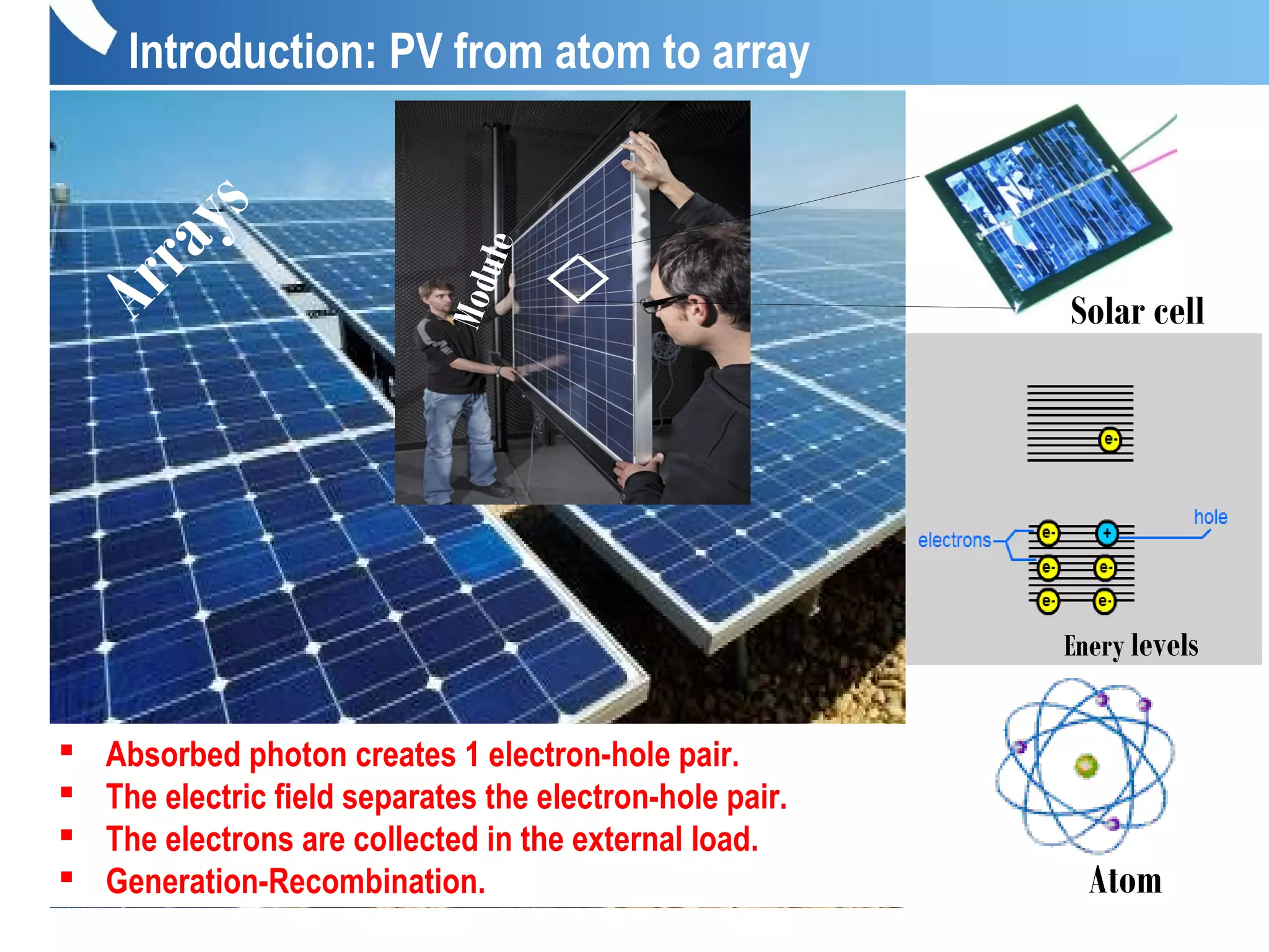
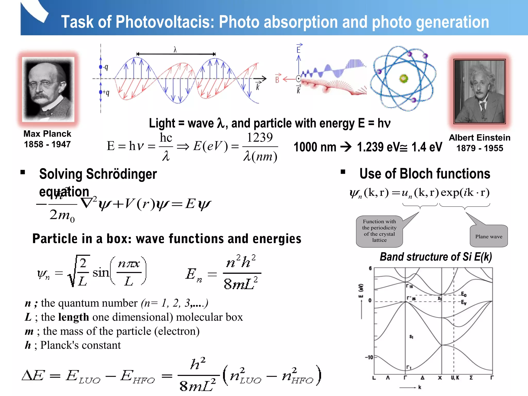
Task of Photovoltacis: Photo absorption and photo generation
1. Light absorption: Generation of free excess
2. Charge separation:
a) Photocurrent, I [A] (Ampere)
b) Photovoltage, V [V] (Volt)
3. Recombintion (defect recombination centers)
V[A] x I[V] = Power [Watt]
Light flux
Valence band
Conduction band](https://image.slidesharecdn.com/lectureourzazateennaouimarch-130519070157-phpapp02/75/Lecture-Conference-Ourzazate-ennaoui-9-2048.jpg)
![Ahmed Ennaoui / Helmholtz-Zentrum Berlin für Materialien und Energie
We need to use most of the solar spectrum: Tandem solar cells
Power [Watt/cm2
] = Voltage [Volt ] x Current density [A/cm2
]
Materials with small Band gap
But low voltage
Excess energy lost to heat
Generating a large current (JSC)
Materials with large band gap
But low current
Sub-band gap light is lost
Generating a large voltage (VOC)
Solar cell
versus
Solar spectrum](https://image.slidesharecdn.com/lectureourzazateennaouimarch-130519070157-phpapp02/75/Lecture-Conference-Ourzazate-ennaoui-18-2048.jpg)
![Photocurrent analysis: Quantum efficiency measurments
Acceptor
Voc
x = 0 La= 1/α
x = Ln
x = W
EJ σ=
dx
dp
Dp
Donor
Rec
µh
µeE
→
p∇
→
Load
• How much light converted?
• Limited information on the electronic properties
• Information on the optical properties of the device
)(R λ−
=
1
EQE
IQE
λ
hc
e
J
Φ
EQE
)(
)(
1 λ
λ
=
This ratio can be measured
Ahmed Ennaoui / Helmholtz-Zentrum Berlin für Materialien und Energie
Φ 0
x R λ
Φ
0
[ ]
[ ]Joulehν
Watt/cmΦ
N
2
photons
in =
[ ]
[ ]Coulombe
A/cmJ
N
2
electrons
out =
Electrons
collected
Photons
absorbed
Φ 0
x Rλ
h(c/λ) < EG
x
0 ).eR.(1ΦΦ α
λ
−
−=
Φ
0](https://image.slidesharecdn.com/lectureourzazateennaouimarch-130519070157-phpapp02/75/Lecture-Conference-Ourzazate-ennaoui-24-2048.jpg)
![EQE and and absorption coefficient
Photon absorption
direct band-gap
( ) GG
2
1
E)E(hνvs..hν →−α
2
G )E(h
hν
B
−= να
Direct Bandgap Eg
EC
EV
Photon
Conduction
Band
Valence
Band
E(k)
GaAse.g.
+k-k
Photon absorption
indirect band-gap
( ) GG
2
E)E(hvs..h →−ννα
2
1
G )E(h
h
A
−= ν
ν
α
Photon
+k-k
Eg
EC
EV
Conduction
Band
Valence
Band
Phonon
EG+Ep
Ep
E(k)
Sie.g.
Ahmed Ennaoui / Helmholtz-Zentrum Berlin für Materialien und Energie and IRESEN
Cut-off λ vs. EG
[eV]E
1.24
m][μλ
G
G =
∫Φ=
λ
λλλ dEQEqJsc )()(
λ
hc
e
J
Φ
EQE
)(
)(
1 λ
λ
=](https://image.slidesharecdn.com/lectureourzazateennaouimarch-130519070157-phpapp02/75/Lecture-Conference-Ourzazate-ennaoui-25-2048.jpg)
![Design to high efficiency solar cells
Light trapping
Reflection Loss: ARC
Material Parameter absorption
Important cost factor €/kg
+
−−= −αW
p
e
αL1
1
1R)(1η
λ
hc
e
)J(
Φ(λ)
1 λ
η =
Decisive Material Parameter
The band gap
0.3 0.5 0.7 0.9 1.1
20
0
40
60
80
100
0
1
2
3
4
5
NumberofSunlightPhotons(m-2
s-1
micron-1
)E+19
RExternalQuantumEfficiency,%
µc-Si:H junctiona-Si:H junction
AM 1.5 global spectrum
Wavelength, microns
a-Si:H/µc-Si:H Cell Spectral Response
Textured TCO
a-Si
Top cell
Back Reflector
Glass substrate
Thin film mc-Si
Bottom cell
[ ]∫ λ−=
GE
λ0λsc dλ.dα-exp.)().ΦR(1.η(λ).qJ
Light from the sun
Ahmed Ennaoui / Helmholtz-Zentrum Berlin für Materialien und Energie and IRESEN](https://image.slidesharecdn.com/lectureourzazateennaouimarch-130519070157-phpapp02/75/Lecture-Conference-Ourzazate-ennaoui-28-2048.jpg)

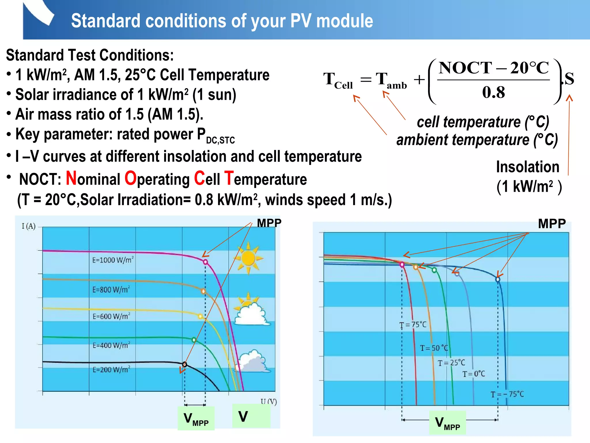
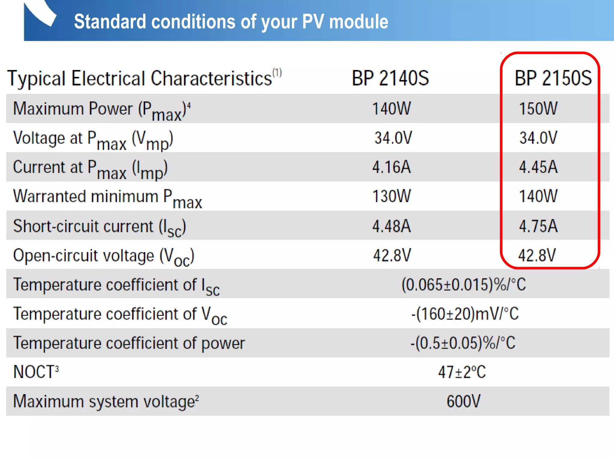
![A. Ennaoui / Helmholtz-Zentrum Berlin für Materialien und Energie
Impact of Cell Temperature on Power for a PV Module.
Estimate cell temperature, open-circuit voltage, and maximum power output for the
150-W BP2150S module under conditions of 1-sun insolation and ambient
temperature 30°C. The module has a NOCT of 47°C.
C64.1
0.8
C204
3.S
0.8
C20NOCT
TT ambCell °=
°−
+=
°−
+=
7
0
From The table for this module at the standard T = 25°C, VOC = 42.8V
VOC drops by about 0.37% per °C , the new VOC = 42.8[1 − 0.0037(64 − 25)] = 36.7 V
with decrease in maximum power available of about 0.5%/°C.
With maximum power expected to drop about 0.5%/°C, this 150-W module at
its maximum power point will deliver:
Pmax = 150 W· [1 − 0.005(64 − 25)] = 121 W
This is a significant drop of 19% from its rated power.
Standard conditions of your PV module](https://image.slidesharecdn.com/lectureourzazateennaouimarch-130519070157-phpapp02/75/Lecture-Conference-Ourzazate-ennaoui-43-2048.jpg)
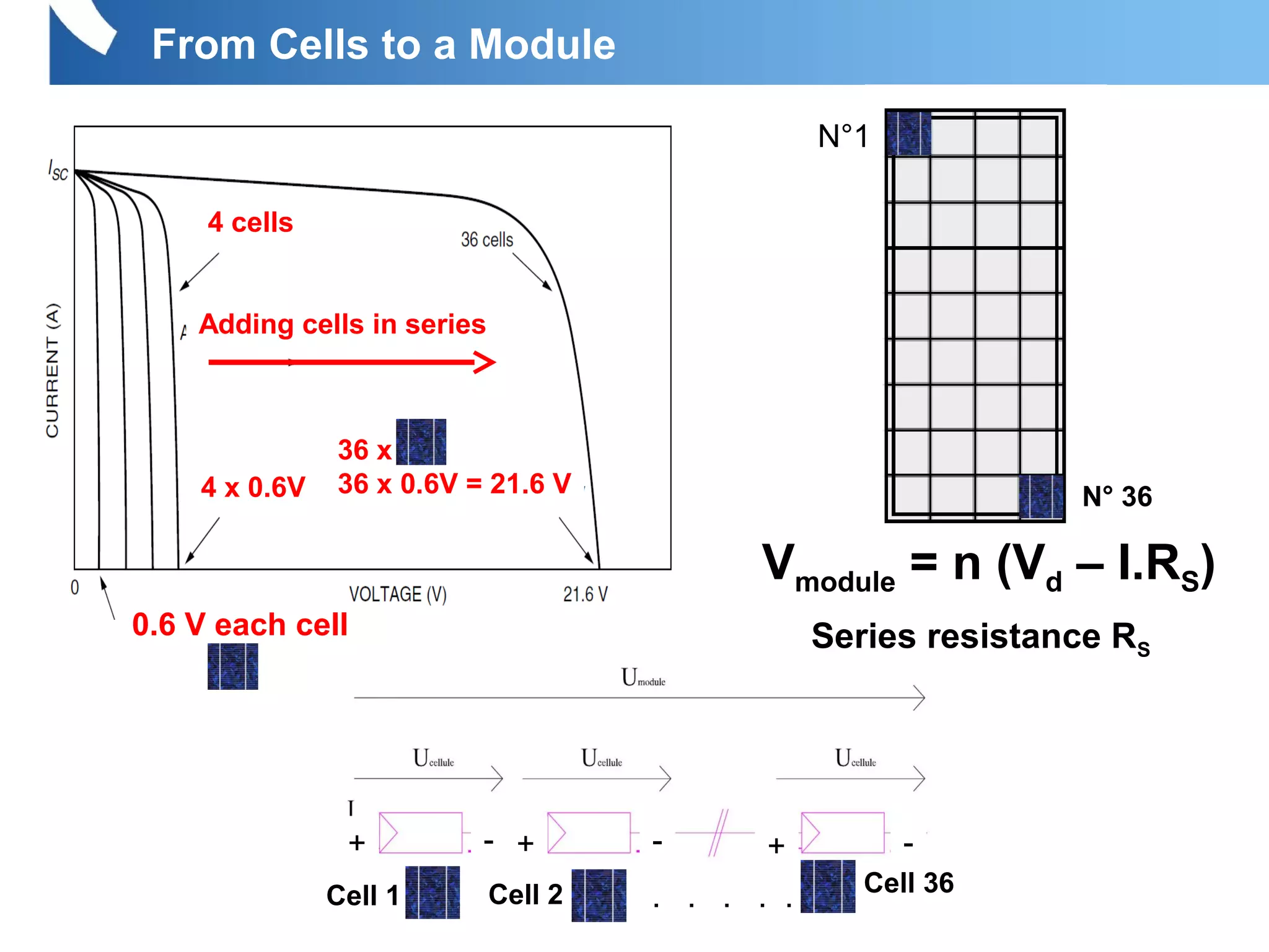
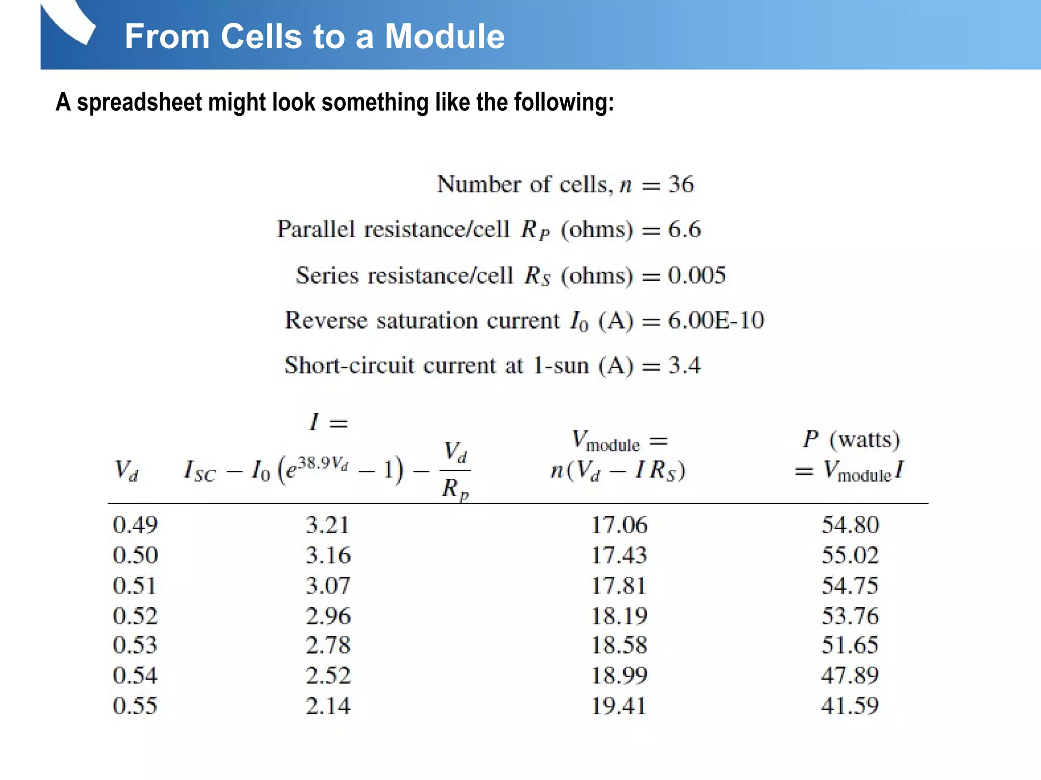
![PV module made up of 36 identical cells, all wired in series. With 1-sun insolation
(1 kW/m2
), each cell has short-circuit current ISC = 3.4 A and at 25°C its reverse saturation
current is I0 = 6 × 10⁻¹⁰
A. Parallel resistance RP = 6.6 Ω and series resistance RS = 0.005Ω .
a) Find the voltage, current, and power delivered when the junction voltage of each cell is
0.50 V.
b) Set up a spreadsheet for I and V and present a few lines of output to show how it works.
Using Vd = 0.50 V along with the other data
The voltage produced by the 36-cell module:
Vmodule = n(Vd − I x RS ) = 36(0.50 − 3.16 x 0.005) = 17.43 V
Power dilevred:
P(watts) = Vmodule x I = 17.43 × 3.16 = 55.0 W
R
I.RV
1
n.k.T
)I . Rq(V
exp.-III
p
SS
0ph
+
−
−
−
=
[ ]
p
dV9.38
0ph
R
V
1e.-III d
−−=
[ ] A6.3
6.6
5.0
1e.10x6-4.3I 5.0x9.3810
=−−= −
Voltage and Current from a PV Module](https://image.slidesharecdn.com/lectureourzazateennaouimarch-130519070157-phpapp02/75/Lecture-Conference-Ourzazate-ennaoui-53-2048.jpg)

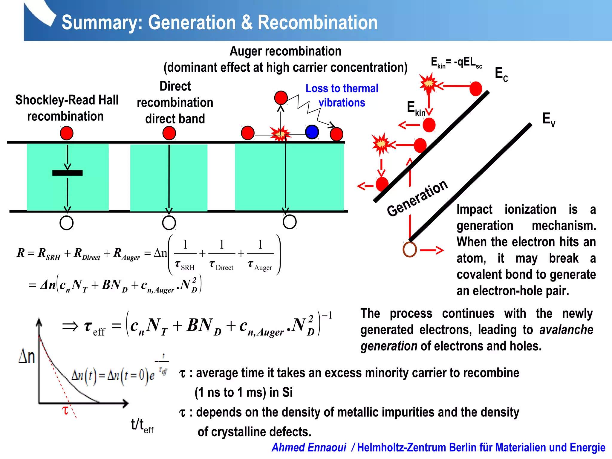
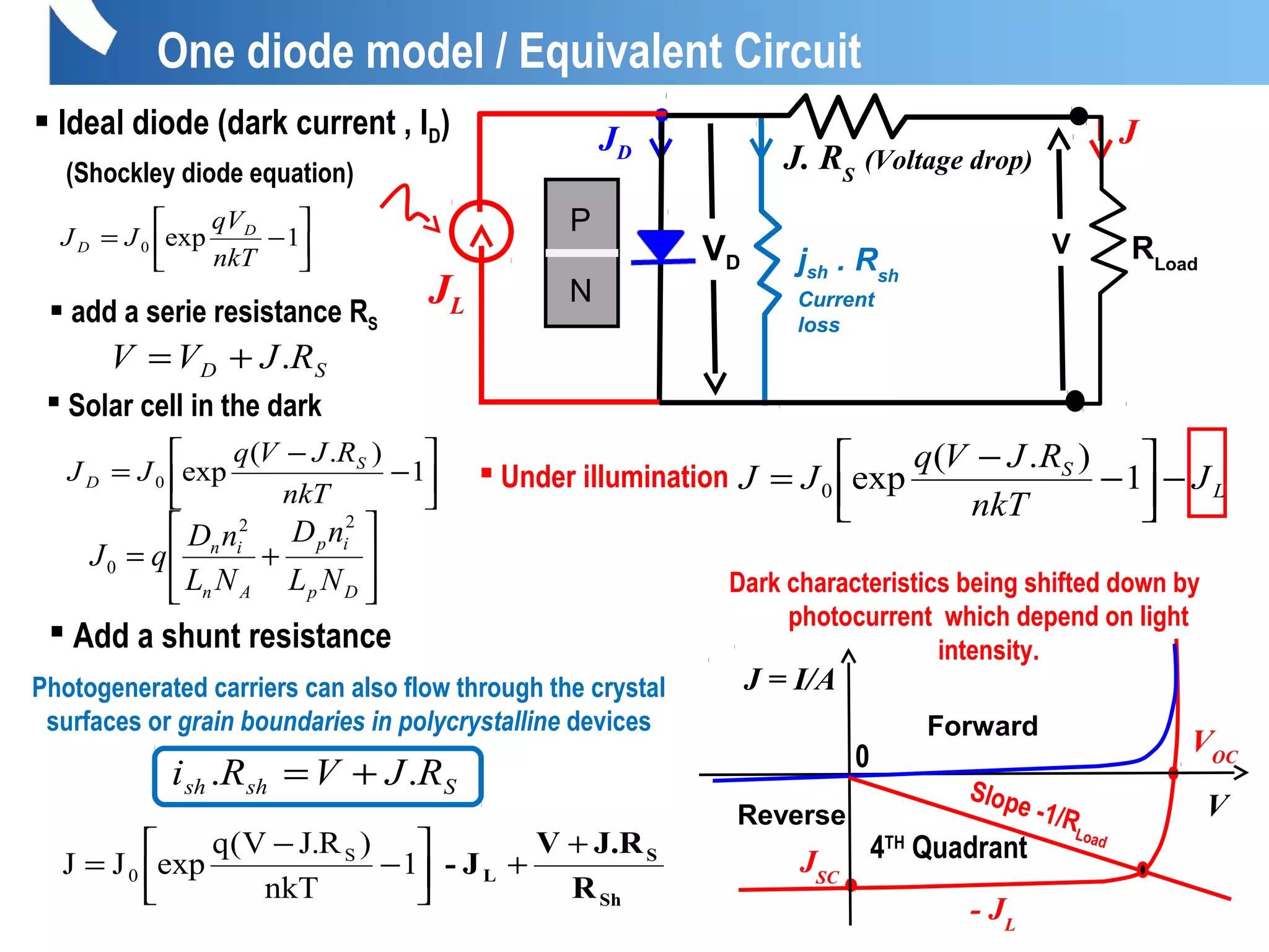
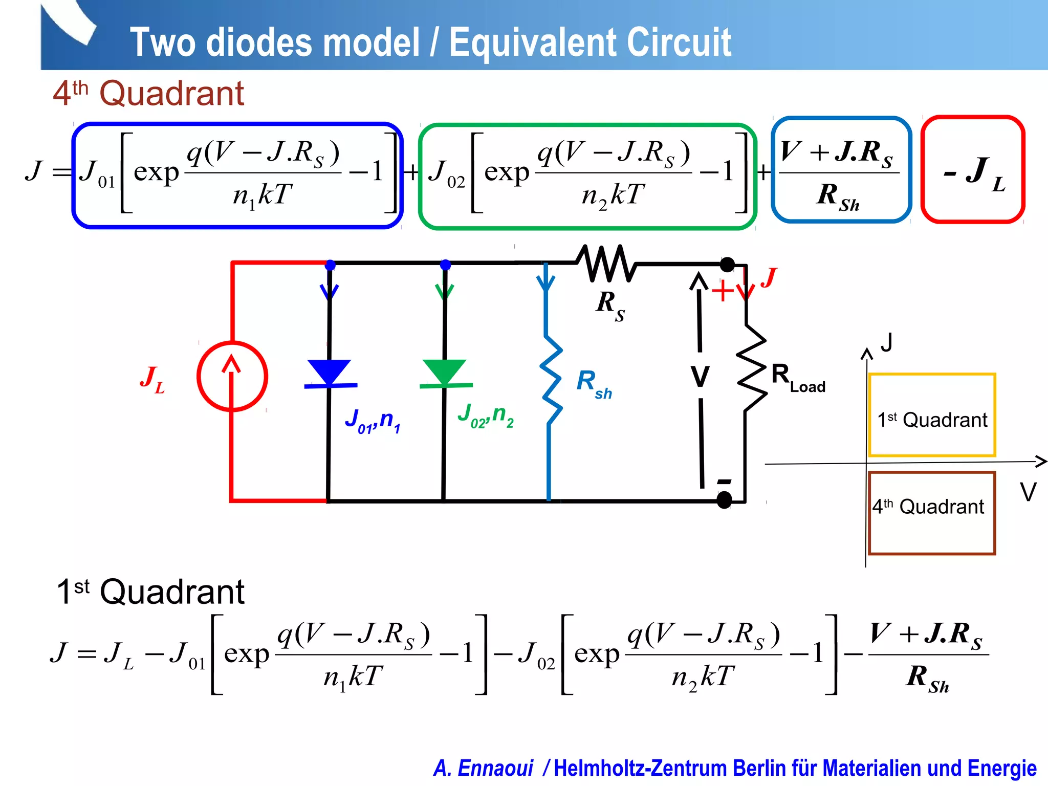
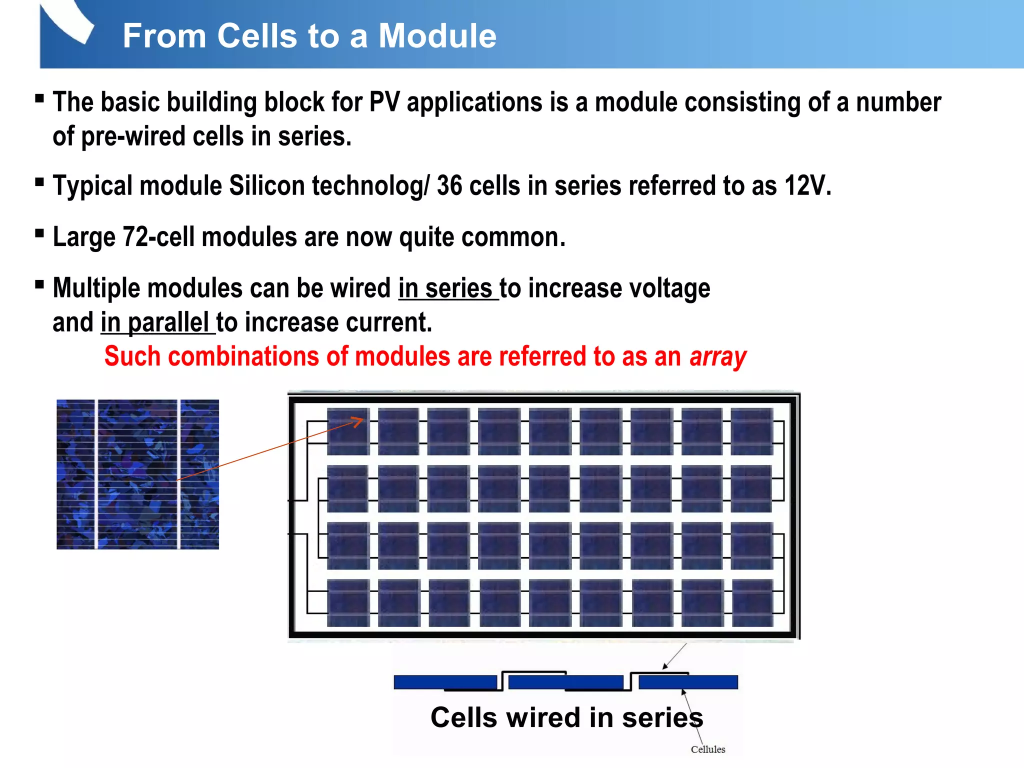
1) The document discusses the basics of solar photovoltaic technology from the atomic level to full solar arrays. It covers topics like photo absorption and generation, energy levels, band structure, doping, p-n junction formation, and device fabrication for both crystalline silicon and thin film solar cell technologies. 2) The document then discusses generation and recombination processes in solar cells like radiative, non-radiative, Auger and Shockley-Read-Hall recombination and how they impact efficiency. It also covers the continuity equation and transport processes. 3) Finally, the basic one diode equivalent circuit model for solar cells is presented along with the Shockley diode equation and how it relates to the current-


![Vibe Coding vs. Spec-Driven Development [Free Meetup]](https://cdn.slidesharecdn.com/ss_thumbnails/vibecodingvsspecdrivendevelopment-251209105622-43f455e7-thumbnail.jpg?width=640&height=640&fit=bounds)


