Downloaded 77 times
![Auxiliary: 27 turns of #38 AWG, two layers 0.002” mylar tape Auxiliary: 27 berubah dari # 38
AWG, dua lapis 0,002 "milar tape
Secondary: 8 turns of #26 AWG, triple insulated wire Sekunder: 8 berubah dari # 26 AWG, triple
kawat terisolasi
Gap: 0.137 mm for a primary inductance of 2.002 mH Gap: 0,137 mm untuk induktansi primer mH
2,002
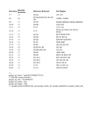
[Schematic diagram source: ON Semiconductor Application Notes] [Diagram skematik sumber: ON
Semiconductor Application Notes]
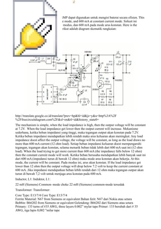
Sopir dioda laser dapat diimplementasikan dengan menggunakan tegangan sumber arus yang
dikendalikan. Linier sederhana ini dioda laser driver memberikan dorongan arus bersih dari
switched (PWM) driver. Here is the schematic diagram of the circuit: Berikut adalah diagram
skematik rangkaian:
A Howland current pump with a current booster is used as the basic of this laser diode driver.
Sebuah Howland pompa arus dengan penguat arus digunakan sebagai dasar dioda laser ini sopir. Q1
is used as the current booster on the output of a RR CMOS OPA350 op amp (U2). P1 digunakan
sebagai penguat arus pada output dari CMOS OPA350 RR op amp (U2). Voltage drop across a
shunt resistor (RSHUNT) in series with the laser diode is measured differentially to sense the
current. Jatuh tegangan shunt resistor (RSHUNT) secara seri dengan dioda laser diukur secara
berbeda-beda untuk merasakan arus. An analog voltage from a potentiometer of from a
microprocessor controlled DAC can be fed to VIN to control the laser diode current. Using the
component values as shown, the scale factor is 1V input equals 1A output. Tegangan analog dari
potensiometer dari dari sebuah mikroprosesor dikendalikan DAC dapat diberikan kepada VIN
untuk mengontrol arus dioda laser. Dengan menggunakan nilai-nilai komponen seperti yang
ditunjukkan, faktor skala 1V input sama dengan output 1A. Other values of scale factor
(VIN/IOUT) can be set by choosing different resistor values using the equation: Nilai-nilai lain
faktor skala (VIN / IOUT) dapat diatur dengan memilih nilai resistor yang berbeda menggunakan
persamaan:](https://image.slidesharecdn.com/rangkaianps-091103203214-phpapp02/85/Rangkaian-Ps-2-320.jpg)
![VIN/IOUT=RSHUNT(R3/R4), with R1=R3, and R2=R4. VIN / IOUT = RSHUNT (R3/R4),
dengan R1 = R3, dan R2 = R4.
[Circuit schematic diagram source: Burr-Brown Products Application Report] [Circuit Diagram
skematik sumber: Burr-Brown Produk Aplikasi Laporan]
<!--
google_ad_client = "pub-0915750066772116";
/* 336x280, created 8/24/08 */
google_ad_slot = "6155698255";
google_ad_width = 336;
google_ad_height = 280;
//-->google_protectAndRun("ads_core.google_render_ad", google_handleError, google_render_ad);
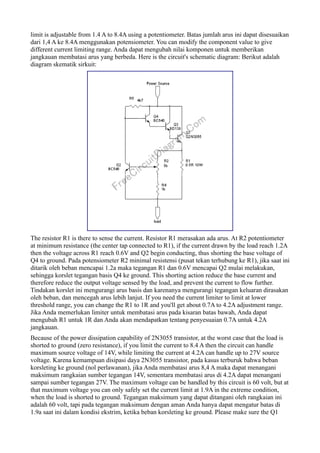
SMP ini AC-DC konverter memberikan efisiensi yang baik. Test data shows efficiency of 83.2% at
115 Vac input and 6A output current, and 85.4% at 230 Vac input and 6A output current. Data
pengujian menunjukkan efisiensi 83,2% pada input dan 115 Vac 6A arus keluaran, dan 85,4% pada
230 Vac 6A input dan arus keluaran. Moreover, the input voltage range is universal, accommodating
92 to 276 Vac variation with only 24 mV change in the output voltage. Selain itu, rentang tegangan
input bersifat universal, menampung 92-276 Vac variasi dengan hanya 24 mV perubahan tegangan
keluaran. Here is the schematic diagram of the circuit: Berikut adalah diagram skematik rangkaian:
C8, C11 = Sanyo Os–Con #16SA1000M, 1000 µF/16V. C8, C11 = Sanyo Os-Con #
16SA1000M, 1000 μF/16V.
C12 =Sanyo Os–Con #10SA150M, 100 µF/16V. C12 = Sanyo Os-Con # 10SA150M,
100 μF/16V.
IC1 =MC33374 mounted on Aavid #604953B02500 extruded heatsink. IC1 = MC33374
dipasang pada Aavid # 604953B02500 diekstrusi heatsink. The heatsink must be drilled
and tapped to allow device & PCB attachment. Keping pendingin yang harus mengebor
dan mengetuk untuk memungkinkan perangkat & PCB lampiran.
Z1 =1.5KE200A with cathode lead soldered in the center of a 5/8” x 3/4” x 0.025” thick
U–shaped copper heatsink. Z1 = 1.5KE200A dengan katoda timah patri di tengah-
tengah 5 / 8 "x 3 / 4" x 0,025 "tebal berbentuk U tembaga heatsink.
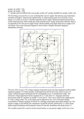
D7 =MBR20100 mounted on Aavid #590302B03600 heatsink. D7 = MBR20100](https://image.slidesharecdn.com/rangkaianps-091103203214-phpapp02/85/Rangkaian-Ps-3-320.jpg)
![dipasang pada Aavid # 590302B03600 heatsink.
L1 =Coilcraft PCV–0–332–10, 3.3 µH, 0.005 ohm. L1 = Coilcraft PCV-0-332-10, 3.3
μH, 0,005 ohm.
T1 = T1 =
Coilcraft W7518–A Coilcraft W7518-A
Primary: 34 turns of # 24 AWG, Pin 9 = start, Pin 6 = finish. Primer: 34 berubah dari #
24 AWG, Pin 9 = mulai, Pin 6 = selesai.
Two layers 0.002” Mylar tape. Dua lapisan 0,002 "Mylar tape.
Secondary: 5 turns of # 20 AWG, 2 strands bifilar wound, Pins 4 and 5 = start, Pins 1
and 2 = finish. Sekunder: 5 putaran dari # 20 AWG, 2 helai bifilar luka, Pin 4 dan 5 =
mulai, Pin 1 dan 2 = selesai.
Two layers 0.002” Mylar tape. Dua lapisan 0,002 "Mylar tape.
Auxiliary: 4 turns of #24 AWG wound in center of bobbin, Pin 10 = start, Pin7 = finish.
Auxiliary: 4 berubah dari # 24 AWG luka di tengah-tengah gelendong, Pin 10 = mulai,
Pin7 = selesai.
Two layers 0.002” Mylar tape. Dua lapisan 0,002 "Mylar tape.
Gap: 0.022” total for a primary inductance (LP) of 290 µH, with a primary to secondary
leakage inductance of 7.2 µH. Gap: 0,022 "total induktansi primer (LP) dari 290 μH,
dengan dasar sampai menengah kebocoran induktansi 7,2 μH.
Core: TDK PC40 EI28Z, PC40 material. Core: EI28Z TDK PC40, PC40 materi.
Bobbin: TDK BE–28–1110CPL, Pins 3 and 8 removed. Gelendong: TDK
BE-28-1110CPL, Pin 3 dan 8 dihapus.
Toggling off PB1 power push button at Vin= 115 Vac result in 0.07 W power consumption, and
0.17W at Vin= 230 Vac. This very low power consumption in the off state is environmentally
friendly. Toggling off tombol daya PB1 di Vin = 115 Vac mengakibatkan konsumsi daya 0,07 W,
dan 0.17W di Vin = 230 Vac. Hal ini sangat rendah konsumsi daya di negara off ramah lingkungan.
[Schematic diagram source: Motorola Analog IC Device Data] [Diagram skematik sumber: LG
Analog IC Device Data]
DC-AC Inverter, Convert 12V DC Voltage untuk Voltage
110/220V AC
DC ke AC inverter rangkaian yang ditunjukkan dalam skema di sini adalah rangkaian sangat
sederhana karena menghasilkan gelombang persegi, tapi itu cukup untuk kekuasaan banyak
perangkat. Here is the schematic diagram of the inverter circuit: Berikut adalah diagram skematik
rangkaian inverter:](https://image.slidesharecdn.com/rangkaianps-091103203214-phpapp02/85/Rangkaian-Ps-4-320.jpg)
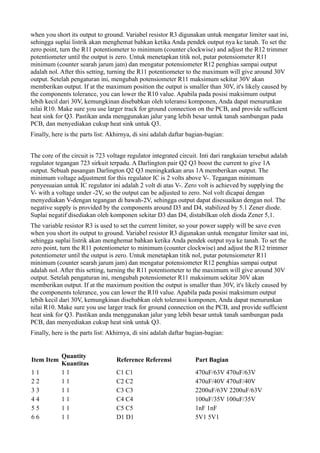
![The MOSFET is configured as bridge, so the current will flow alternatively in through the primary
windings of the transformer. Yang MOSFET dikonfigurasi sebagai jembatan, sehingga arus akan
mengalir alternatif dalam melalui gulungan primer dari transformator. The most expensive part of
this dc-ac inverter circuit is the transformer, since it must handle high current up to 10 Amps. Yang
paling mahal ini bagian dari inverter dc-ac rangkaian trafo, karena harus menangani arus tinggi
hingga 10 Amps. You can power any device up to 120 Watts using this 12V inverter circuit. Anda
dapat daya perangkat apapun hingga 120 Watts menggunakan rangkaian inverter 12V ini.
<!--
google_ad_client = "pub-0915750066772116";
/* 336x280, created 8/24/08 */
google_ad_slot = "6155698255";
google_ad_width = 336;
google_ad_height = 280;
//-->google_protectAndRun("ads_core.google_render_ad", google_handleError, google_render_ad);
Menggunakan variabel Power Supply Switching Regulator
Jika Anda seorang penggemar atau elektronik profesional insinyur yang membuat banyak elektronik
e] percobaan, pemecahan masalah, atau tes, menyediakan berbagai variabel tegangan pasokan listrik
di laboratorium atau workshop Anda akan membuat hidup Anda lebih mudah. You can build your
variable power supply using linear adjustable regulator, but switching technology let you design a
very wide voltage adjustment range without loosing the efficiency too much. Anda dapat
membangun catu daya variabel menggunakan adjustable regulator linier, tapi teknologi switching
membiarkan Anda desain yang sangat luas rentang penyesuaian tegangan efisiensi tanpa kehilangan
terlalu banyak. Switching regulator is used in this variable voltage power supply circuit to preserve
the efficiency around 70%. Here is the schematic diagram of the circuit: Switching regulator
digunakan dalam variabel ini sirkuit listrik tegangan untuk mempertahankan efisiensi sekitar 70%.
Berikut ini adalah diagram skematik rangkaian:](https://image.slidesharecdn.com/rangkaianps-091103203214-phpapp02/85/Rangkaian-Ps-5-320.jpg)
![The heart of this variable power supply is the LM2575 integrated circuit chip from National
Semiconductor. Jantung catu daya variabel ini adalah sirkuit terintegrasi LM2575 chip dari National
Semiconductor. This IC gives you a very simple design, require only few external components. The
optional filter shown in the dashed line box is recommended for cleaner voltage output, give the
best performance for lab requirement. IC ini memberikan desain yang sangat sederhana, hanya
memerlukan beberapa komponen eksternal. Penyaring opsional ditampilkan pada kotak garis putus-
putus dianjurkan untuk tegangan output yang bersih, memberikan performa terbaik untuk
kebutuhan laboratorium. A grounded metal box is recommended for this variable power supply
casing, since it elliminate the EMI radiation. Sebuah kotak logam grounded dianjurkan untuk catu
daya variabel ini casing, karena radiasi elliminate EMI. Using a grounded metal case will make sure
that your power supply cicruit won't violate FCC rules regarding EMI radiation. Menggunakan
kasus logam grounded akan memastikan bahwa Anda akan cicruit listrik tidak melanggar aturan
FCC tentang radiasi EMI. [Source: National Semiconductor Application Notes] [Sumber: National
Semiconductor Application Notes]
Efisiensi tinggi 3.3V Mode Switch 5A Langkah-Down
Converter
Mode switch ini langkah-down Konverter memiliki efisiensi yang sangat baik, hingga 94% dapat
diperoleh. This switch mode regulator uses LTC1266-3.3 controller with external N-Channel power
mosfet, and need only a 5uH inductor because it uses high frequency switching. Mode switch ini
regulator LTC1266-3.3 menggunakan controller dengan eksternal kekuasaan N-Channel MOSFET,](https://image.slidesharecdn.com/rangkaianps-091103203214-phpapp02/85/Rangkaian-Ps-6-320.jpg)
![dan hanya memerlukan sebuah 5uH induktor karena switching menggunakan frekuensi tinggi. Here
is the schematic diagram of this switch mode step down converter circuit: Berikut adalah diagram
skematik modus switch ini turun rangkaian konverter:
To optimize efficiency, the LTC1266 automatically switches between two modes of operation,
burst and continuous. Untuk mengoptimalkan efisiensi, LTC1266 secara otomatis beralih di antara
dua mode operasi, meledak dan berkesinambungan. The LTC1266 series uses a current mode,
constant off-time architecture to synchronously switch an external pair of power MOSFETs. Seri
yang LTC1266 menggunakan mode aktif, konstan waktu off-arsitektur untuk serentak mengalihkan
kekuasaan sepasang eksternal MOSFET. Operating frequency is set by an external capacitor at the
timing capacitor Pin 6. Operasi frekuensi diatur oleh kapasitor eksternal pada waktu kapasitor Pin 6.
[Circuit's schematic diagram source: Linear Technology Application Notes] [Circuit's skematik
diagram sumber: Linear Technology Application Notes]
Variabel (Adjustable) Current Limiter Sirkuit
Advertisement: Advertisement:
Sirkuit ini menyediakan otomatis membatasi arus sampai 8.4A. Unlike current limiter that uses only
a resistor, this current limiting circuit doesn't drop the voltage, or at least keep the voltage drop at
minimum, until a certain current amount is exceeded. Tidak seperti saat ini hanya limiter yang
menggunakan resistor, arus ini tidak membatasi rangkaian drop tegangan, atau setidaknya tetap
jatuh tegangan minimal, sampai jumlah tertentu yang telah terlampaui saat ini. This current amount](https://image.slidesharecdn.com/rangkaianps-091103203214-phpapp02/85/Rangkaian-Ps-7-320.jpg)
![transistor has sufficient heat sink. Harap pastikan transistor Q1 telah cukup heat sink. [Circuit
Schematic Source: Designed by FreeCircuitDiagram.Com] [Circuit Schematic Sumber: Designed
by FreeCircuitDiagram.Com]
Adjustable 0-30V Power Supply
Adjustable 0-30V Power Supply
Hal pertama yang Anda harus memiliki di bengkel / laboratorium adalah listrik. In experimenting
many new electronic circuit design, it is easier if you have a flexible adjustable power supply.
Dalam percobaan banyak desain sirkuit elektronik baru, lebih mudah jika Anda memiliki power
supply disesuaikan fleksibel. Here is an adjustable 0-30 volts power supply design. Berikut adalah
yang dapat diatur power supply 0-30 volt desain. The circuit schematic diagram is shown below.
Diagram skematik rangkaian ditampilkan di bawah.
Sponsored Links Sponsored Links
<!--
google_ad_client = "pub-0915750066772116";
/* 160x90, created 9/5/08 */
google_ad_slot = "1100755785";
google_ad_width = 160;
google_ad_height = 90;](https://image.slidesharecdn.com/rangkaianps-091103203214-phpapp02/85/Rangkaian-Ps-9-320.jpg)


1. Rangkaian ini dapat digunakan untuk mengisi baterai secara efisien dengan menyediakan tegangan konstan 7,2V atau arus konstan 600 mA. 2. Skema sirkuit menggunakan regulator tegangan atau arus konstan untuk menjaga keluaran tetap terlepas dari beban. 3. Rangkaian ini dapat menyediakan daya untuk perangkat dengan daya hingga 120W.


