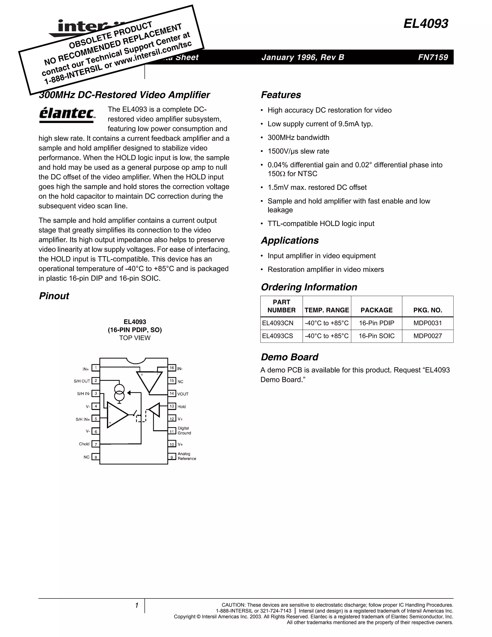
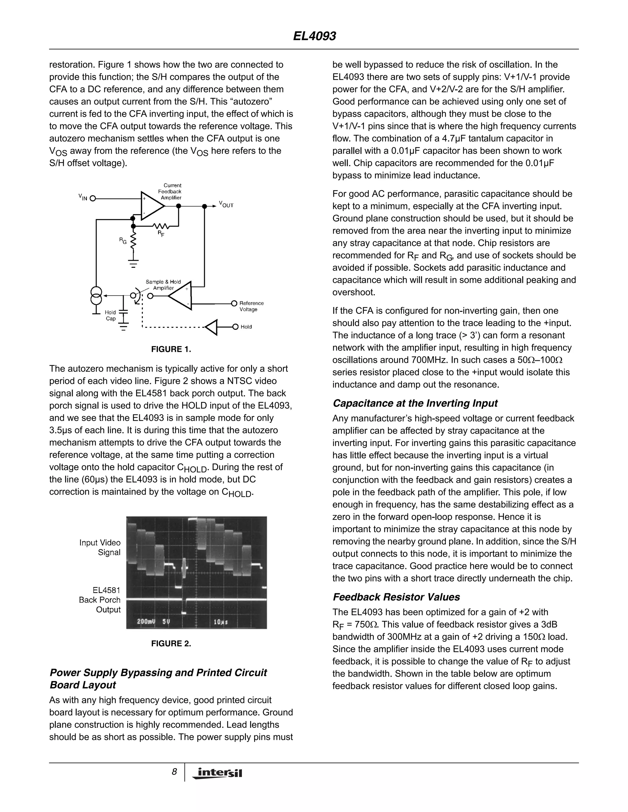
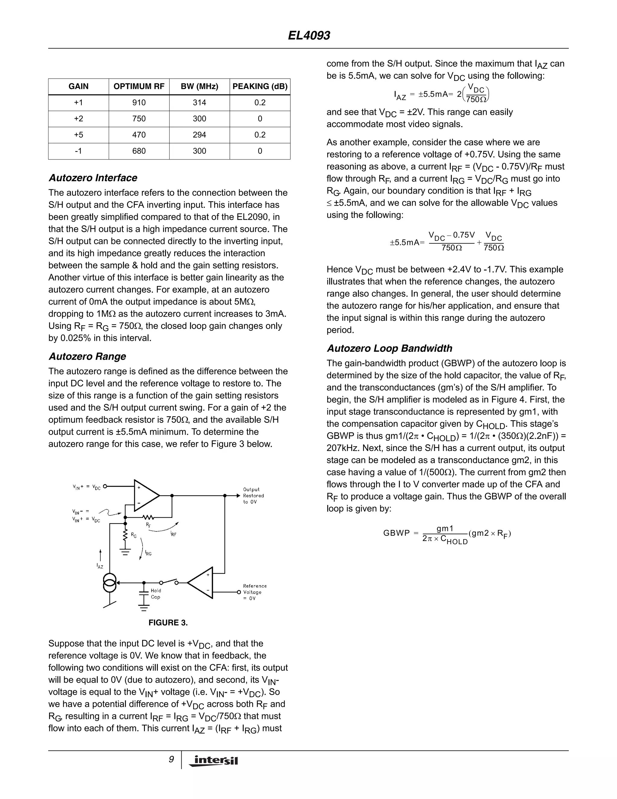
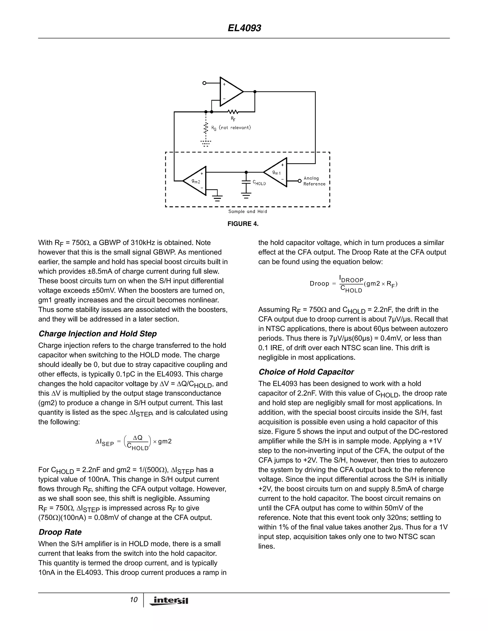
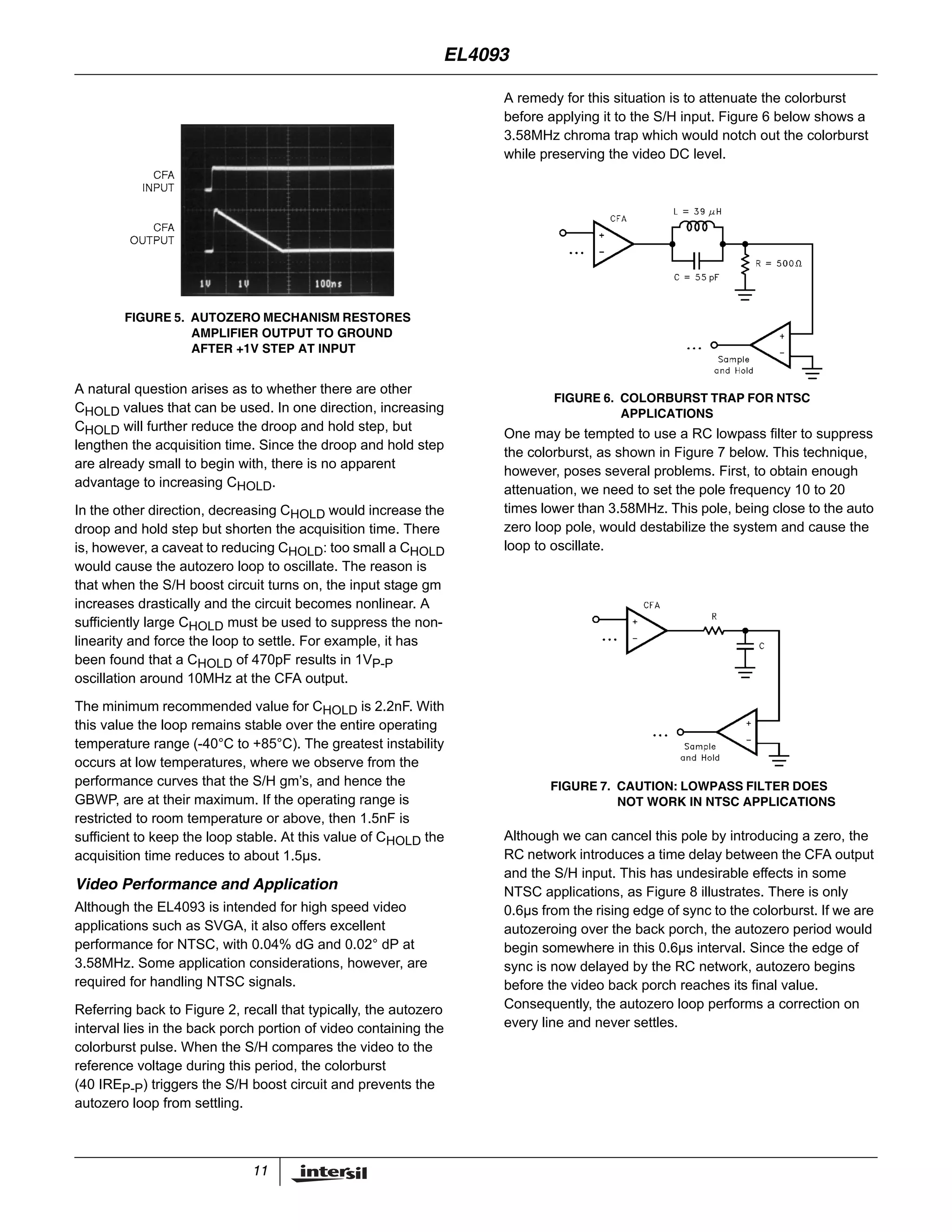
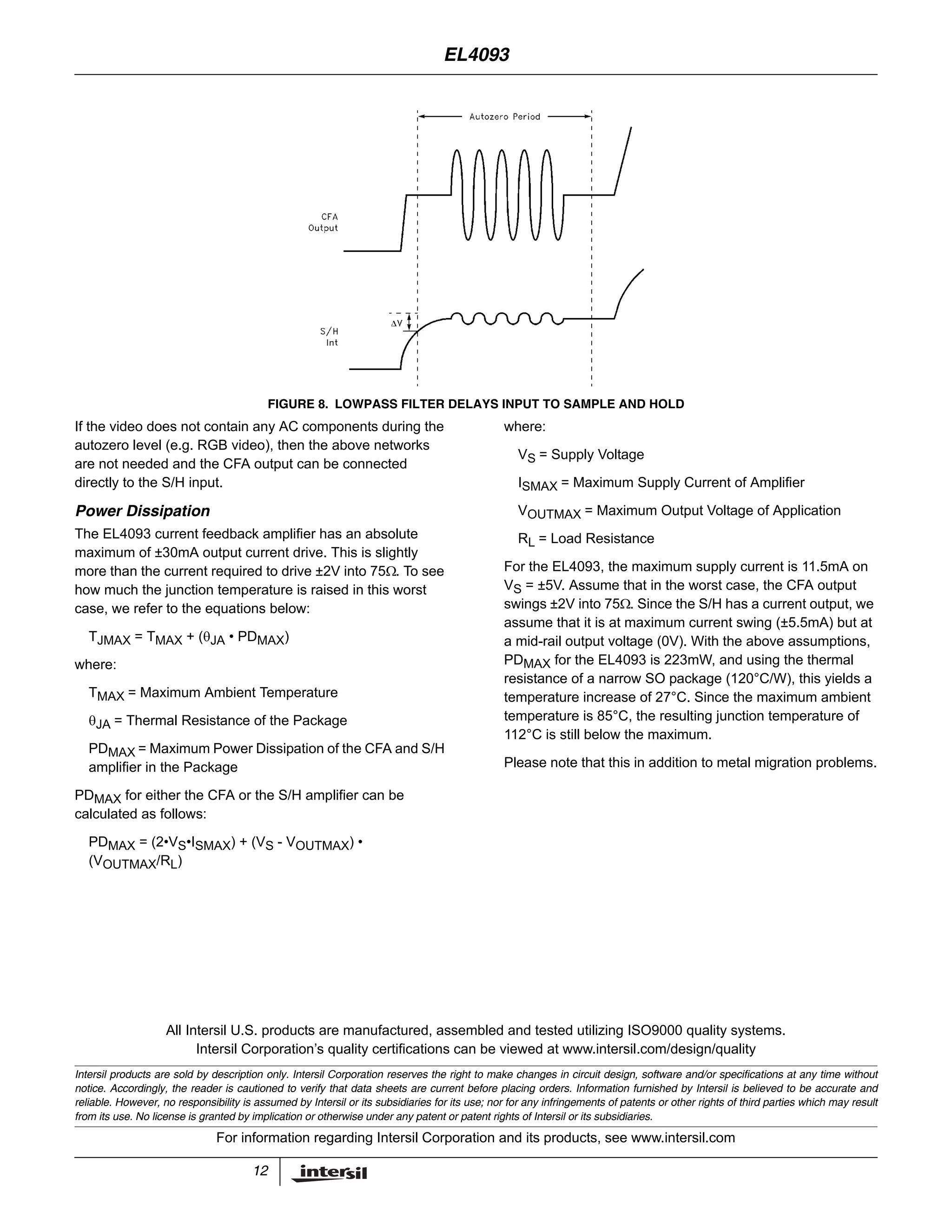
SlideShare a Scribd company logo
1
®
FN7159
CAUTION: These devices are sensitive to electrostatic discharge; follow proper IC Handling Procedures.
1-888-INTERSIL or 321-724-7143 | Intersil (and design) is a registered trademark of Intersil Americas Inc.
Copyright © Intersil Americas Inc. 2003. All Rights Reserved. Elantec is a registered trademark of Elantec Semiconductor, Inc.
All other trademarks mentioned are the property of their respective owners.
EL4093
300MHz DC-Restored Video Amplifier
The EL4093 is a complete DC-
restored video amplifier subsystem,
featuring low power consumption and
high slew rate. It contains a current feedback amplifier and a
sample and hold amplifier designed to stabilize video
performance. When the HOLD logic input is low, the sample
and hold may be used as a general purpose op amp to null
the DC offset of the video amplifier. When the HOLD input
goes high the sample and hold stores the correction voltage
on the hold capacitor to maintain DC correction during the
subsequent video scan line.
The sample and hold amplifier contains a current output
stage that greatly simplifies its connection to the video
amplifier. Its high output impedance also helps to preserve
video linearity at low supply voltages. For ease of interfacing,
the HOLD input is TTL-compatible. This device has an
operational temperature of -40°C to +85°C and is packaged
in plastic 16-pin DIP and 16-pin SOIC.
Pinout
Features
• High accuracy DC restoration for video
• Low supply current of 9.5mA typ.
• 300MHz bandwidth
• 1500V/µs slew rate
• 0.04% differential gain and 0.02° differential phase into
150Ω for NTSC
• 1.5mV max. restored DC offset
• Sample and hold amplifier with fast enable and low
leakage
• TTL-compatible HOLD logic input
Applications
• Input amplifier in video equipment
• Restoration amplifier in video mixers
Demo Board
A demo PCB is available for this product. Request “EL4093
Demo Board.”
EL4093
(16-PIN PDIP, SO)
TOP VIEW
Ordering Information
PART
NUMBER TEMP. RANGE PACKAGE PKG. NO.
EL4093CN -40°C to +85°C 16-Pin PDIP MDP0031
EL4093CS -40°C to +85°C 16-Pin SOIC MDP0027
Data Sheet January 1996, Rev B
OBSOLETE PRODUCT
NO RECOMMENDED REPLACEMENT
contact our Technical Support Center at
1-888-INTERSIL or www.intersil.com/tsc
2
Absolute Maximum Ratings (TA = 25°C)
VS V+ to V- Supply Voltage . . . . . . . . . . . . . . . . . . . . . . . . 12.6V
VHOLDVoltage at HOLD input
(DGND-0.7) to (DGND+5.5V)
VIN Voltage at any other input . . . . . . . . . . . . . . . . . . . . . V+ to V-
ΔVIN Difference between Sample and Hold inputs . . . . . . . . . .±8V
IOUT1 Video amplifier output current . . . . . . . . . . . . . . . . . . . ±30mA
IOUT2 S/H amplifier output current . . . . . . . . . . . . . . . . . . . . ±10mA
IIN Maximum current into other pins. . . . . . . . . . . . . . . . . . ±6mA
PD Maximum Power Dissipation. . . . . . . . . . . . . . . . See Curves
TA Operating Ambient Temperature Range . . . . .-40°C to +85°C
TJ Operating Junction Temperature. . . . . . . . . . . . . . . . . . 150°C
TST Storage Temperature Range. . . . . . . . . . . . .-65°C to +150°C
CAUTION: Stresses above those listed in “Absolute Maximum Ratings” may cause permanent damage to the device. This is a stress only rating and operation of the
device at these or any other conditions above those indicated in the operational sections of this specification is not implied.
IMPORTANT NOTE: All parameters having Min/Max specifications are guaranteed. Typical values are for information purposes only. Unless otherwise noted, all tests
are at the specified temperature and are pulsed tests, therefore: TJ = TC = TA
Open-Loop DC Electrical Specifications Power supplies at ±5V, TA = 25°C
Sample and Hold
PARAMETER DESCRIPTION MIN TYP MAX UNITS
IS,HOLD Total Supply current in HOLD mode 9.5 11.5 mA
IS,SAMPLE Total Supply current in SAMPLE mode 8.5 10.5 mA
Video Amplifier Section (Not Restored)
PARAMETER DESCRIPTION MIN TYP MAX UNITS
VOS Input Offset Voltage 10 110 mV
IB+ Non-Inverting Input Bias Current 10 25 µA
IB- Inverting Input Bias Current 15 50 µA
ROL Transimpedance, VOUT = ±2.5V, RL = 150Ω 150 400 kΩ
VO Output Voltage Swing, RL = 150Ω ±3 ±3.5 V
ISC Output Short-Circuit Current 60 100 mA
Open-Loop DC Electrical Specifications Power supplies at ±5V, TA = 25°C
Sample and Hold Section
PARAMETER DESCRIPTION MIN TYP MAX UNITS
VOS Input Offset Voltage 0.5 1.5 mV
TCVOS Average Offset Voltage Drift 6 µV/°C
IB Input Bias Current 1 2 µA
IOS Input Offset Current 10 200 nA
TCIOS Average Offset Current Drift 0.1 nA/°C
VCM Common Mode Input Range ±2.5 ±2.8 V
gM Transconductance (RL = 500Ω) 5 15 A/V
CMRR Common Mode Rejection Ratio (VCM -2.5V to +2.5V) 70 90 dB
VIL HOLD Logic Input Low (referenced to Digital GND) 0.8 V
VIH HOLD Logic Input High (referenced to Digital GND) 2.0 V
VGND Digital GND Reference Voltage (V-) (V+) - 4.0 V
IDROOP Hold Mode Droop Current 10 70 nA
ICHARGE Charge Current Available to CHOLD ±5.5 ±8.5 mA
VO Output Voltage Swing (RL = 10kΩ) ±3 ±3.5 V
IO Output Current Swing (RL = 0Ω) ±4.5 ±5.5 mA
EL4093
3
Typical Application
Closed-Loop AC Electrical Specifications Power supplies at ±5V, TA = 25°C, RF = RG = 750Ω, RL = 150Ω, CL = 5pF, CIN-
(parasitic) = 1.8pF
Video Amplifier Section
PARAMETER DESCRIPTION MIN TYP MAX UNITS
BW, -3dB -3dB Small-Signal Bandwidth 300 MHz
BW, ±0.1dB 0.1dB Flatness Bandwidth 50 MHz
Peaking Frequency Response Peaking 0 dB
SR Slew rate, VOUT between -2V and +2V 1500 V/µs
dG Differential Gain Error, Voffset between -714mV and +714mV 0.04 %
dθ Differential Phase Error, Voffset between -714mV and +714mV 0.02 °
Closed-Loop AC Electrical Specifications Power supplies at ±5V, TA = 25°C, RF = RG = 750Ω, RL = 150Ω, CL = 5pF,
CHOLD = 2.2nF
Sample and Hold Section
PARAMETER DESCRIPTION MIN TYP MAX UNITS
ΔISTEP Change in Sample to Hold Output Current Due to Hold Step 0.1 µA
ΔTSH Sample to Hold Delay Time 15 ns
ΔTHS Hold to Sample Delay Time 40 ns
TAC Settling Time to 1% (DC Restored Amplifier Output) Video Amplifier Input
from 0 to 1V
2.2 µs
EL4093
4
Typical Performance Curves
Non-inverting Frequency
Response (Gain)
Non-inverting Frequency
Response (Phase)
Frequency Response
for Various RL
Frequency Response
for Various CL
Inverting Frequency
Response (Phase)
Inverting Frequency
Response (Gain)
Frequency Response for
Various RF and RG
Frequency Response
for Various CIN
3dB Bandwidth vs
Temperature (Video Amp)
EL4093
5
Typical Performance Curves (Continued)
Peaking vs Temperature
(Video Amp)
Output Voltage
Swing vs Frequency
2nd and 3rd Harmonic
Distortion vs Frequency
Supply Current
vs Temperature
Voltage and Current
Noise vs Frequency
Input Offset Voltage
vs Die Temperature
(Video Amp, 3 Sample)
Input Bias Current vs
Temperature (Video Amp)
Transimpedance vs
Temperature (Video Amp)
EL4093
6
Typical Performance Curves (Continued)
Input Offset Voltage
vs Die Temperature
(Sample & Hold, 3 Samples)
Input Bias Current vs
Die Temperature
(Sample & Hold)
Transconductance vs
Temperature (Sample & Hold)
Output Current Swing vs
Temperature (Sample & Hold)
Transconductance vs
Die Temperature
(Sample & Hold)
Droop Current
vs Temperature
(Sample & Hold)
Charge Current vs
Temperature
(Sample & Hold)
Hold Step (ΔIOUT)
vs Temperature
EL4093
7
Typical Performance Curves (Continued)
Applications Information
Product Description
The EL4093 is a high speed DC-restore system containing a
current feedback amplifier (CFA) and a sample & hold (S/H)
amplifier. The CFA offers a wide 3dB bandwidth of 300MHz
and a slew rate of 1500V/µs, making it ideal for high speed
video applications such as SVGA. The CFA’s excellent
differential gain and phase at 3.58MHz also makes it suitable
for NTSC applications. Drawing only 9.5mA on ±5V supplies,
the EL4093 serves as an excellent choice for those
applications requiring both low power and high bandwidth.
The connection between the CFA and sample & hold (the
Autozero interface) has been greatly simplified. The output
of the sample & hold is a high impedance current source,
allowing direct connection to the CFA inverting input for
autozero purposes. In addition, special circuitry within the
sample & hold provides a charge current of 8.5mA in sample
mode, resulting in a sample hold current ratio (ratio of
charging current to droop current) of approx. 1,000,000.
Theory of Operation
In video applications, DC restoration moves the backporch
or black level to a fixed DC reference. The EL4093 uses a
CFA in feedback with a sample & hold to provide DC
Differential Gain and
Phase vs DC Input
Voltage at 3.58MHz
Differential Gain and
Phase vs DC Input
Voltage at 3.58MHz
Slew Rate vs Die
Temperature (Video Amp)
Small-Signal Step Response Large-Signal Step Response
Settling Time vs
Settling Accuracy
(Video Amp)
Maximum Power Dissipation
vs Ambient Temperature,
16-Pin PDIP Package
Maximum Power Dissipation
vs Ambient Temperature,
16-Pin SO Package
EL4093
8
restoration. Figure 1 shows how the two are connected to
provide this function; the S/H compares the output of the
CFA to a DC reference, and any difference between them
causes an output current from the S/H. This “autozero”
current is fed to the CFA inverting input, the effect of which is
to move the CFA output towards the reference voltage. This
autozero mechanism settles when the CFA output is one
VOS away from the reference (the VOS here refers to the
S/H offset voltage).
The autozero mechanism is typically active for only a short
period of each video line. Figure 2 shows a NTSC video
signal along with the EL4581 back porch output. The back
porch signal is used to drive the HOLD input of the EL4093,
and we see that the EL4093 is in sample mode for only
3.5µs of each line. It is during this time that the autozero
mechanism attempts to drive the CFA output towards the
reference voltage, at the same time putting a correction
voltage onto the hold capacitor CHOLD. During the rest of
the line (60µs) the EL4093 is in hold mode, but DC
correction is maintained by the voltage on CHOLD.
Power Supply Bypassing and Printed Circuit
Board Layout
As with any high frequency device, good printed circuit
board layout is necessary for optimum performance. Ground
plane construction is highly recommended. Lead lengths
should be as short as possible. The power supply pins must
be well bypassed to reduce the risk of oscillation. In the
EL4093 there are two sets of supply pins: V+1/V-1 provide
power for the CFA, and V+2/V-2 are for the S/H amplifier.
Good performance can be achieved using only one set of
bypass capacitors, although they must be close to the
V+1/V-1 pins since that is where the high frequency currents
flow. The combination of a 4.7µF tantalum capacitor in
parallel with a 0.01µF capacitor has been shown to work
well. Chip capacitors are recommended for the 0.01µF
bypass to minimize lead inductance.
For good AC performance, parasitic capacitance should be
kept to a minimum, especially at the CFA inverting input.
Ground plane construction should be used, but it should be
removed from the area near the inverting input to minimize
any stray capacitance at that node. Chip resistors are
recommended for RF and RG, and use of sockets should be
avoided if possible. Sockets add parasitic inductance and
capacitance which will result in some additional peaking and
overshoot.
If the CFA is configured for non-inverting gain, then one
should also pay attention to the trace leading to the +input.
The inductance of a long trace (> 3’) can form a resonant
network with the amplifier input, resulting in high frequency
oscillations around 700MHz. In such cases a 50Ω–100Ω
series resistor placed close to the +input would isolate this
inductance and damp out the resonance.
Capacitance at the Inverting Input
Any manufacturer’s high-speed voltage or current feedback
amplifier can be affected by stray capacitance at the
inverting input. For inverting gains this parasitic capacitance
has little effect because the inverting input is a virtual
ground, but for non-inverting gains this capacitance (in
conjunction with the feedback and gain resistors) creates a
pole in the feedback path of the amplifier. This pole, if low
enough in frequency, has the same destabilizing effect as a
zero in the forward open-loop response. Hence it is
important to minimize the stray capacitance at this node by
removing the nearby ground plane. In addition, since the S/H
output connects to this node, it is important to minimize the
trace capacitance. Good practice here would be to connect
the two pins with a short trace directly underneath the chip.
Feedback Resistor Values
The EL4093 has been optimized for a gain of +2 with
RF = 750Ω. This value of feedback resistor gives a 3dB
bandwidth of 300MHz at a gain of +2 driving a 150Ω load.
Since the amplifier inside the EL4093 uses current mode
feedback, it is possible to change the value of RF to adjust
the bandwidth. Shown in the table below are optimum
feedback resistor values for different closed loop gains.
FIGURE 1.
FIGURE 2.
EL4093
9
Autozero Interface
The autozero interface refers to the connection between the
S/H output and the CFA inverting input. This interface has
been greatly simplified compared to that of the EL2090, in
that the S/H output is a high impedance current source. The
S/H output can be connected directly to the inverting input,
and its high impedance greatly reduces the interaction
between the sample & hold and the gain setting resistors.
Another virtue of this interface is better gain linearity as the
autozero current changes. For example, at an autozero
current of 0mA the output impedance is about 5MΩ,
dropping to 1MΩ as the autozero current increases to 3mA.
Using RF = RG = 750Ω, the closed loop gain changes only
by 0.025% in this interval.
Autozero Range
The autozero range is defined as the difference between the
input DC level and the reference voltage to restore to. The
size of this range is a function of the gain setting resistors
used and the S/H output current swing. For a gain of +2 the
optimum feedback resistor is 750Ω, and the available S/H
output current is ±5.5mA minimum. To determine the
autozero range for this case, we refer to Figure 3 below.
Suppose that the input DC level is +VDC, and that the
reference voltage is 0V. We know that in feedback, the
following two conditions will exist on the CFA: first, its output
will be equal to 0V (due to autozero), and second, its VIN-
voltage is equal to the VIN+ voltage (i.e. VIN- = +VDC). So
we have a potential difference of +VDC across both RF and
RG, resulting in a current IRF = IRG = VDC/750Ω that must
flow into each of them. This current IAZ = (IRF + IRG) must
come from the S/H output. Since the maximum that IAZ can
be is 5.5mA, we can solve for VDC using the following:
and see that VDC = ±2V. This range can easily
accommodate most video signals.
As another example, consider the case where we are
restoring to a reference voltage of +0.75V. Using the same
reasoning as above, a current IRF = (VDC - 0.75V)/RF must
flow through RF, and a current IRG = VDC/RG must go into
RG. Again, our boundary condition is that IRF + IRG
≤ ±5.5mA, and we can solve for the allowable VDC values
using the following:
Hence VDC must be between +2.4V to -1.7V. This example
illustrates that when the reference changes, the autozero
range also changes. In general, the user should determine
the autozero range for his/her application, and ensure that
the input signal is within this range during the autozero
period.
Autozero Loop Bandwidth
The gain-bandwidth product (GBWP) of the autozero loop is
determined by the size of the hold capacitor, the value of RF,
and the transconductances (gm’s) of the S/H amplifier. To
begin, the S/H amplifier is modeled as in Figure 4. First, the
input stage transconductance is represented by gm1, with
the compensation capacitor given by CHOLD. This stage’s
GBWP is thus gm1/(2π • CHOLD) = 1/(2π • (350Ω)(2.2nF)) =
207kHz. Next, since the S/H has a current output, its output
stage can be modeled as a transconductance gm2, in this
case having a value of 1/(500Ω). The current from gm2 then
flows through the I to V converter made up of the CFA and
RF to produce a voltage gain. Thus the GBWP of the overall
loop is given by:
GAIN OPTIMUM RF BW (MHz) PEAKING (dB)
+1 910 314 0.2
+2 750 300 0
+5 470 294 0.2
-1 680 300 0
FIGURE 3.
IAZ 5.5mA 2
VDC
750Ω
---------------
⎝ ⎠
⎛ ⎞=±=
5.5mA
VDC 0.75V–
750Ω
----------------------------------
VDC
750Ω
---------------+=±
GBWP
gm1
2π CHOLD×
--------------------------------- gm2 RF×( )=
EL4093
10
With RF = 750Ω, a GBWP of 310kHz is obtained. Note
however that this is the small signal GBWP. As mentioned
earlier, the sample and hold has special boost circuits built in
which provides ±8.5mA of charge current during full slew.
These boost circuits turn on when the S/H input differential
voltage exceeds ±50mV. When the boosters are turned on,
gm1 greatly increases and the circuit becomes nonlinear.
Thus some stability issues are associated with the boosters,
and they will be addressed in a later section.
Charge Injection and Hold Step
Charge injection refers to the charge transferred to the hold
capacitor when switching to the HOLD mode. The charge
should ideally be 0, but due to stray capacitive coupling and
other effects, is typically 0.1pC in the EL4093. This charge
changes the hold capacitor voltage by ΔV = ΔQ/CHOLD, and
this ΔV is multiplied by the output stage transconductance
(gm2) to produce a change in S/H output current. This last
quantity is listed as the spec ΔISTEP, and is calculated using
the following:
For CHOLD = 2.2nF and gm2 = 1/(500Ω), ΔISTEP has a
typical value of 100nA. This change in S/H output current
flows through RF, shifting the CFA output voltage. However,
as we shall soon see, this shift is negligible. Assuming
RF = 750Ω, ΔISTEP is impressed across RF to give
(750Ω)(100nA) = 0.08mV of change at the CFA output.
Droop Rate
When the S/H amplifier is in HOLD mode, there is a small
current that leaks from the switch into the hold capacitor.
This quantity is termed the droop current, and is typically
10nA in the EL4093. This droop current produces a ramp in
the hold capacitor voltage, which in turn produces a similar
effect at the CFA output. The Droop Rate at the CFA output
can be found using the equation below:
Assuming RF = 750Ω and CHOLD = 2.2nF, the drift in the
CFA output due to droop current is about 7µV/µs. Recall that
in NTSC applications, there is about 60µs between autozero
periods. Thus there is 7µV/µs(60µs) = 0.4mV, or less than
0.1 IRE, of drift over each NTSC scan line. This drift is
negligible in most applications.
Choice of Hold Capacitor
The EL4093 has been designed to work with a hold
capacitor of 2.2nF. With this value of CHOLD, the droop rate
and hold step are negligibly small for most applications. In
addition, with the special boost circuits inside the S/H, fast
acquisition is possible even using a hold capacitor of this
size. Figure 5 shows the input and output of the DC-restored
amplifier while the S/H is in sample mode. Applying a +1V
step to the non-inverting input of the CFA, the output of the
CFA jumps to +2V. The S/H, however, then tries to autozero
the system by driving the CFA output back to the reference
voltage. Since the input differential across the S/H is initially
+2V, the boost circuits turn on and supply 8.5mA of charge
current to the hold capacitor. The boost circuit remains on
until the CFA output has come to within 50mV of the
reference. Note that this event took only 320ns; settling to
within 1% of the final value takes another 2µs. Thus for a 1V
input step, acquisition takes only one to two NTSC scan
lines.
FIGURE 4.
ΔISEP
ΔQ
CHOLD
--------------------
⎝ ⎠
⎛ ⎞ gm2×=
Droop
IDROOP
CHOLD
---------------------- gm2 RF×( )=
EL4093
11
A natural question arises as to whether there are other
CHOLD values that can be used. In one direction, increasing
CHOLD will further reduce the droop and hold step, but
lengthen the acquisition time. Since the droop and hold step
are already small to begin with, there is no apparent
advantage to increasing CHOLD.
In the other direction, decreasing CHOLD would increase the
droop and hold step but shorten the acquisition time. There
is, however, a caveat to reducing CHOLD: too small a CHOLD
would cause the autozero loop to oscillate. The reason is
that when the S/H boost circuit turns on, the input stage gm
increases drastically and the circuit becomes nonlinear. A
sufficiently large CHOLD must be used to suppress the non-
linearity and force the loop to settle. For example, it has
been found that a CHOLD of 470pF results in 1VP-P
oscillation around 10MHz at the CFA output.
The minimum recommended value for CHOLD is 2.2nF. With
this value the loop remains stable over the entire operating
temperature range (-40°C to +85°C). The greatest instability
occurs at low temperatures, where we observe from the
performance curves that the S/H gm’s, and hence the
GBWP, are at their maximum. If the operating range is
restricted to room temperature or above, then 1.5nF is
sufficient to keep the loop stable. At this value of CHOLD the
acquisition time reduces to about 1.5µs.
Video Performance and Application
Although the EL4093 is intended for high speed video
applications such as SVGA, it also offers excellent
performance for NTSC, with 0.04% dG and 0.02° dP at
3.58MHz. Some application considerations, however, are
required for handling NTSC signals.
Referring back to Figure 2, recall that typically, the autozero
interval lies in the back porch portion of video containing the
colorburst pulse. When the S/H compares the video to the
reference voltage during this period, the colorburst
(40 IREP-P) triggers the S/H boost circuit and prevents the
autozero loop from settling.
A remedy for this situation is to attenuate the colorburst
before applying it to the S/H input. Figure 6 below shows a
3.58MHz chroma trap which would notch out the colorburst
while preserving the video DC level.
One may be tempted to use a RC lowpass filter to suppress
the colorburst, as shown in Figure 7 below. This technique,
however, poses several problems. First, to obtain enough
attenuation, we need to set the pole frequency 10 to 20
times lower than 3.58MHz. This pole, being close to the auto
zero loop pole, would destabilize the system and cause the
loop to oscillate.
Although we can cancel this pole by introducing a zero, the
RC network introduces a time delay between the CFA output
and the S/H input. This has undesirable effects in some
NTSC applications, as Figure 8 illustrates. There is only
0.6µs from the rising edge of sync to the colorburst. If we are
autozeroing over the back porch, the autozero period would
begin somewhere in this 0.6µs interval. Since the edge of
sync is now delayed by the RC network, autozero begins
before the video back porch reaches its final value.
Consequently, the autozero loop performs a correction on
every line and never settles.
FIGURE 5. AUTOZERO MECHANISM RESTORES
AMPLIFIER OUTPUT TO GROUND
AFTER +1V STEP AT INPUT
FIGURE 6. COLORBURST TRAP FOR NTSC
APPLICATIONS
FIGURE 7. CAUTION: LOWPASS FILTER DOES
NOT WORK IN NTSC APPLICATIONS
EL4093
12
All Intersil U.S. products are manufactured, assembled and tested utilizing ISO9000 quality systems.
Intersil Corporation’s quality certifications can be viewed at www.intersil.com/design/quality
Intersil products are sold by description only. Intersil Corporation reserves the right to make changes in circuit design, software and/or specifications at any time without
notice. Accordingly, the reader is cautioned to verify that data sheets are current before placing orders. Information furnished by Intersil is believed to be accurate and
reliable. However, no responsibility is assumed by Intersil or its subsidiaries for its use; nor for any infringements of patents or other rights of third parties which may result
from its use. No license is granted by implication or otherwise under any patent or patent rights of Intersil or its subsidiaries.
For information regarding Intersil Corporation and its products, see www.intersil.com
If the video does not contain any AC components during the
autozero level (e.g. RGB video), then the above networks
are not needed and the CFA output can be connected
directly to the S/H input.
Power Dissipation
The EL4093 current feedback amplifier has an absolute
maximum of ±30mA output current drive. This is slightly
more than the current required to drive ±2V into 75Ω. To see
how much the junction temperature is raised in this worst
case, we refer to the equations below:
TJMAX = TMAX + (θJA • PDMAX)
where:
TMAX = Maximum Ambient Temperature
θJA = Thermal Resistance of the Package
PDMAX = Maximum Power Dissipation of the CFA and S/H
amplifier in the Package
PDMAX for either the CFA or the S/H amplifier can be
calculated as follows:
PDMAX = (2•VS•ISMAX) + (VS - VOUTMAX) •
(VOUTMAX/RL)
where:
VS = Supply Voltage
ISMAX = Maximum Supply Current of Amplifier
VOUTMAX = Maximum Output Voltage of Application
RL = Load Resistance
For the EL4093, the maximum supply current is 11.5mA on
VS = ±5V. Assume that in the worst case, the CFA output
swings ±2V into 75Ω. Since the S/H has a current output, we
assume that it is at maximum current swing (±5.5mA) but at
a mid-rail output voltage (0V). With the above assumptions,
PDMAX for the EL4093 is 223mW, and using the thermal
resistance of a narrow SO package (120°C/W), this yields a
temperature increase of 27°C. Since the maximum ambient
temperature is 85°C, the resulting junction temperature of
112°C is still below the maximum.
Please note that this in addition to metal migration problems.
FIGURE 8. LOWPASS FILTER DELAYS INPUT TO SAMPLE AND HOLD
EL4093

More Related Content

What's hot

Mosfet irfz44 n 1 philips semiconductors
Mosfet irfz44 n 1 philips semiconductorsMosfet irfz44 n 1 philips semiconductors
Mosfet irfz44 n 1 philips semiconductors
Alfa Gama Omega
 
3 channel thermocouple thermometer
3 channel thermocouple thermometer3 channel thermocouple thermometer
3 channel thermocouple thermometerIsmanu Rahadi
 
Original Opto LTV-354T LTV354T 354T 354 SOP-4 New
Original Opto LTV-354T LTV354T 354T 354 SOP-4 NewOriginal Opto LTV-354T LTV354T 354T 354 SOP-4 New
Original Opto LTV-354T LTV354T 354T 354 SOP-4 New
AUTHELECTRONIC
 
Tl431
Tl431Tl431
Datasheet ni
Datasheet niDatasheet ni
Datasheet ni
Nguyễn Khánh
 
Transistor mosfet to220 - psmn005
Transistor mosfet   to220 - psmn005Transistor mosfet   to220 - psmn005
Transistor mosfet to220 - psmn005
Samuel Borges
 
Stk4192 stereo aplifier
Stk4192 stereo aplifierStk4192 stereo aplifier
Stk4192 stereo aplifier
hliaslat
 
Original Opto TLP701 P701 701 SOP-6 New Toshiba
Original Opto TLP701 P701 701 SOP-6 New ToshibaOriginal Opto TLP701 P701 701 SOP-6 New Toshiba
Original Opto TLP701 P701 701 SOP-6 New Toshiba
authelectroniccom
 
RT7257E Datasheet PDF
RT7257E Datasheet PDFRT7257E Datasheet PDF
RT7257E Datasheet PDF
Datasheet Bank
 
Original PNP Transistors PZT2907A PZT2907 2907 P2F SOT22-3 New On Semiconductor
Original PNP Transistors PZT2907A PZT2907 2907 P2F SOT22-3 New On SemiconductorOriginal PNP Transistors PZT2907A PZT2907 2907 P2F SOT22-3 New On Semiconductor
Original PNP Transistors PZT2907A PZT2907 2907 P2F SOT22-3 New On Semiconductor
authelectroniccom
 
Bt139
Bt139Bt139
St microelectronics l7815-cv-datasheet
St microelectronics l7815-cv-datasheetSt microelectronics l7815-cv-datasheet
St microelectronics l7815-cv-datasheetcongiodiqua
 
Origianl Opto TLP781 P781 PC781 781 DIP-4 New
Origianl Opto TLP781 P781 PC781 781 DIP-4 NewOrigianl Opto TLP781 P781 PC781 781 DIP-4 New
Origianl Opto TLP781 P781 PC781 781 DIP-4 New
AUTHELECTRONIC
 

What's hot (20)

Mosfet irfz44 n 1 philips semiconductors
Mosfet irfz44 n 1 philips semiconductorsMosfet irfz44 n 1 philips semiconductors
Mosfet irfz44 n 1 philips semiconductors
 
000715
000715000715
000715
 
3 channel thermocouple thermometer
3 channel thermocouple thermometer3 channel thermocouple thermometer
3 channel thermocouple thermometer
 
Original Opto LTV-354T LTV354T 354T 354 SOP-4 New
Original Opto LTV-354T LTV354T 354T 354 SOP-4 NewOriginal Opto LTV-354T LTV354T 354T 354 SOP-4 New
Original Opto LTV-354T LTV354T 354T 354 SOP-4 New
 
Sbos078
Sbos078Sbos078
Sbos078
 
Tl431
Tl431Tl431
Tl431
 
000705
000705000705
000705
 
Datasheet ni
Datasheet niDatasheet ni
Datasheet ni
 
Transistor mosfet to220 - psmn005
Transistor mosfet   to220 - psmn005Transistor mosfet   to220 - psmn005
Transistor mosfet to220 - psmn005
 
Ucc 3895 dw
Ucc 3895 dwUcc 3895 dw
Ucc 3895 dw
 
Stk4192 stereo aplifier
Stk4192 stereo aplifierStk4192 stereo aplifier
Stk4192 stereo aplifier
 
Original Opto TLP701 P701 701 SOP-6 New Toshiba
Original Opto TLP701 P701 701 SOP-6 New ToshibaOriginal Opto TLP701 P701 701 SOP-6 New Toshiba
Original Opto TLP701 P701 701 SOP-6 New Toshiba
 
RT7257E Datasheet PDF
RT7257E Datasheet PDFRT7257E Datasheet PDF
RT7257E Datasheet PDF
 
2 n5401
2 n54012 n5401
2 n5401
 
Bt136 datasheet
Bt136 datasheetBt136 datasheet
Bt136 datasheet
 
Original PNP Transistors PZT2907A PZT2907 2907 P2F SOT22-3 New On Semiconductor
Original PNP Transistors PZT2907A PZT2907 2907 P2F SOT22-3 New On SemiconductorOriginal PNP Transistors PZT2907A PZT2907 2907 P2F SOT22-3 New On Semiconductor
Original PNP Transistors PZT2907A PZT2907 2907 P2F SOT22-3 New On Semiconductor
 
Bt139
Bt139Bt139
Bt139
 
St microelectronics l7815-cv-datasheet
St microelectronics l7815-cv-datasheetSt microelectronics l7815-cv-datasheet
St microelectronics l7815-cv-datasheet
 
Origianl Opto TLP781 P781 PC781 781 DIP-4 New
Origianl Opto TLP781 P781 PC781 781 DIP-4 NewOrigianl Opto TLP781 P781 PC781 781 DIP-4 New
Origianl Opto TLP781 P781 PC781 781 DIP-4 New
 
7818
78187818
7818
 

Viewers also liked

HotGod_MJJMarketing1
HotGod_MJJMarketing1HotGod_MJJMarketing1
HotGod_MJJMarketing1Megan Pickett
 
Dreamweaver
DreamweaverDreamweaver
Ads final project presentation narrated
Ads final project presentation   narratedAds final project presentation   narrated
Ads final project presentation narrated
IsminiTheo
 
Examen salud publica contestado
Examen salud publica contestadoExamen salud publica contestado
Examen salud publica contestado
Shamir123
 
Gerund
GerundGerund
Gerund
Richin Koshy
 
Peranan sektor pertanian
Peranan sektor pertanianPeranan sektor pertanian
Peranan sektor pertanian
epi rizkiyah
 

Viewers also liked (8)

HotGod_MJJMarketing1
HotGod_MJJMarketing1HotGod_MJJMarketing1
HotGod_MJJMarketing1
 
Dreamweaver
DreamweaverDreamweaver
Dreamweaver
 
Ads final project presentation narrated
Ads final project presentation   narratedAds final project presentation   narrated
Ads final project presentation narrated
 
Akbar Ullah_Resume IT
Akbar Ullah_Resume ITAkbar Ullah_Resume IT
Akbar Ullah_Resume IT
 
Examen salud publica contestado
Examen salud publica contestadoExamen salud publica contestado
Examen salud publica contestado
 
Convguaymas2013
Convguaymas2013Convguaymas2013
Convguaymas2013
 
Gerund
GerundGerund
Gerund
 
Peranan sektor pertanian
Peranan sektor pertanianPeranan sektor pertanian
Peranan sektor pertanian
 

Similar to EL4093 Datasheet

As15 f
As15 fAs15 f
Advanced motion controls 30a20ac
Advanced motion controls 30a20acAdvanced motion controls 30a20ac
Advanced motion controls 30a20ac
Electromate
 
Advanced motion controls 50a8
Advanced motion controls 50a8Advanced motion controls 50a8
Advanced motion controls 50a8
Electromate
 
Advanced motion controls 100a40
Advanced motion controls 100a40Advanced motion controls 100a40
Advanced motion controls 100a40
Electromate
 
Advanced motions control 16a20ac
Advanced motions control 16a20acAdvanced motions control 16a20ac
Advanced motions control 16a20ac
Electromate
 
Advanced motion controls 50a20
Advanced motion controls 50a20Advanced motion controls 50a20
Advanced motion controls 50a20
Electromate
 
Advanced motion controls 30a8
Advanced motion controls 30a8Advanced motion controls 30a8
Advanced motion controls 30a8
Electromate
 
Advanced motion controls 100a25
Advanced motion controls 100a25Advanced motion controls 100a25
Advanced motion controls 100a25
Electromate
 
Advanced motion controls azbe40a8
Advanced motion controls azbe40a8Advanced motion controls azbe40a8
Advanced motion controls azbe40a8
Electromate
 
Advanced motion controls 25a20
Advanced motion controls 25a20Advanced motion controls 25a20
Advanced motion controls 25a20
Electromate
 
Advanced motion controls azbh60a8
Advanced motion controls azbh60a8Advanced motion controls azbh60a8
Advanced motion controls azbh60a8
Electromate
 
Advanced motion controls b30a40
Advanced motion controls b30a40Advanced motion controls b30a40
Advanced motion controls b30a40
Electromate
 
Advanced motion controls azbh25a20
Advanced motion controls azbh25a20Advanced motion controls azbh25a20
Advanced motion controls azbh25a20
Electromate
 
BA4510のデータシート(ローム)
BA4510のデータシート(ローム)BA4510のデータシート(ローム)
BA4510のデータシート(ローム)
Tsuyoshi Horigome
 
Advanced motion controls 120a10
Advanced motion controls 120a10Advanced motion controls 120a10
Advanced motion controls 120a10
Electromate
 
Original Opto TLP250 P250 DIP-8 New Toshiba
Original Opto TLP250 P250 DIP-8 New ToshibaOriginal Opto TLP250 P250 DIP-8 New Toshiba
Original Opto TLP250 P250 DIP-8 New Toshiba
AUTHELECTRONIC
 
Tlp2630
Tlp2630Tlp2630
Advanced motion controls az10a20
Advanced motion controls az10a20Advanced motion controls az10a20
Advanced motion controls az10a20
Electromate
 
Advanced motion controls az40a8ddc
Advanced motion controls az40a8ddcAdvanced motion controls az40a8ddc
Advanced motion controls az40a8ddc
Electromate
 
Advanced motion controls be25a20fac
Advanced motion controls be25a20facAdvanced motion controls be25a20fac
Advanced motion controls be25a20fac
Electromate
 

Similar to EL4093 Datasheet (20)

As15 f
As15 fAs15 f
As15 f
 
Advanced motion controls 30a20ac
Advanced motion controls 30a20acAdvanced motion controls 30a20ac
Advanced motion controls 30a20ac
 
Advanced motion controls 50a8
Advanced motion controls 50a8Advanced motion controls 50a8
Advanced motion controls 50a8
 
Advanced motion controls 100a40
Advanced motion controls 100a40Advanced motion controls 100a40
Advanced motion controls 100a40
 
Advanced motions control 16a20ac
Advanced motions control 16a20acAdvanced motions control 16a20ac
Advanced motions control 16a20ac
 
Advanced motion controls 50a20
Advanced motion controls 50a20Advanced motion controls 50a20
Advanced motion controls 50a20
 
Advanced motion controls 30a8
Advanced motion controls 30a8Advanced motion controls 30a8
Advanced motion controls 30a8
 
Advanced motion controls 100a25
Advanced motion controls 100a25Advanced motion controls 100a25
Advanced motion controls 100a25
 
Advanced motion controls azbe40a8
Advanced motion controls azbe40a8Advanced motion controls azbe40a8
Advanced motion controls azbe40a8
 
Advanced motion controls 25a20
Advanced motion controls 25a20Advanced motion controls 25a20
Advanced motion controls 25a20
 
Advanced motion controls azbh60a8
Advanced motion controls azbh60a8Advanced motion controls azbh60a8
Advanced motion controls azbh60a8
 
Advanced motion controls b30a40
Advanced motion controls b30a40Advanced motion controls b30a40
Advanced motion controls b30a40
 
Advanced motion controls azbh25a20
Advanced motion controls azbh25a20Advanced motion controls azbh25a20
Advanced motion controls azbh25a20
 
BA4510のデータシート(ローム)
BA4510のデータシート(ローム)BA4510のデータシート(ローム)
BA4510のデータシート(ローム)
 
Advanced motion controls 120a10
Advanced motion controls 120a10Advanced motion controls 120a10
Advanced motion controls 120a10
 
Original Opto TLP250 P250 DIP-8 New Toshiba
Original Opto TLP250 P250 DIP-8 New ToshibaOriginal Opto TLP250 P250 DIP-8 New Toshiba
Original Opto TLP250 P250 DIP-8 New Toshiba
 
Tlp2630
Tlp2630Tlp2630
Tlp2630
 
Advanced motion controls az10a20
Advanced motion controls az10a20Advanced motion controls az10a20
Advanced motion controls az10a20
 
Advanced motion controls az40a8ddc
Advanced motion controls az40a8ddcAdvanced motion controls az40a8ddc
Advanced motion controls az40a8ddc
 
Advanced motion controls be25a20fac
Advanced motion controls be25a20facAdvanced motion controls be25a20fac
Advanced motion controls be25a20fac
 

EL4093 Datasheet

  • 1. 1 ® FN7159 CAUTION: These devices are sensitive to electrostatic discharge; follow proper IC Handling Procedures. 1-888-INTERSIL or 321-724-7143 | Intersil (and design) is a registered trademark of Intersil Americas Inc. Copyright © Intersil Americas Inc. 2003. All Rights Reserved. Elantec is a registered trademark of Elantec Semiconductor, Inc. All other trademarks mentioned are the property of their respective owners. EL4093 300MHz DC-Restored Video Amplifier The EL4093 is a complete DC- restored video amplifier subsystem, featuring low power consumption and high slew rate. It contains a current feedback amplifier and a sample and hold amplifier designed to stabilize video performance. When the HOLD logic input is low, the sample and hold may be used as a general purpose op amp to null the DC offset of the video amplifier. When the HOLD input goes high the sample and hold stores the correction voltage on the hold capacitor to maintain DC correction during the subsequent video scan line. The sample and hold amplifier contains a current output stage that greatly simplifies its connection to the video amplifier. Its high output impedance also helps to preserve video linearity at low supply voltages. For ease of interfacing, the HOLD input is TTL-compatible. This device has an operational temperature of -40°C to +85°C and is packaged in plastic 16-pin DIP and 16-pin SOIC. Pinout Features • High accuracy DC restoration for video • Low supply current of 9.5mA typ. • 300MHz bandwidth • 1500V/µs slew rate • 0.04% differential gain and 0.02° differential phase into 150Ω for NTSC • 1.5mV max. restored DC offset • Sample and hold amplifier with fast enable and low leakage • TTL-compatible HOLD logic input Applications • Input amplifier in video equipment • Restoration amplifier in video mixers Demo Board A demo PCB is available for this product. Request “EL4093 Demo Board.” EL4093 (16-PIN PDIP, SO) TOP VIEW Ordering Information PART NUMBER TEMP. RANGE PACKAGE PKG. NO. EL4093CN -40°C to +85°C 16-Pin PDIP MDP0031 EL4093CS -40°C to +85°C 16-Pin SOIC MDP0027 Data Sheet January 1996, Rev B OBSOLETE PRODUCT NO RECOMMENDED REPLACEMENT contact our Technical Support Center at 1-888-INTERSIL or www.intersil.com/tsc
  • 2. 2 Absolute Maximum Ratings (TA = 25°C) VS V+ to V- Supply Voltage . . . . . . . . . . . . . . . . . . . . . . . . 12.6V VHOLDVoltage at HOLD input (DGND-0.7) to (DGND+5.5V) VIN Voltage at any other input . . . . . . . . . . . . . . . . . . . . . V+ to V- ΔVIN Difference between Sample and Hold inputs . . . . . . . . . .±8V IOUT1 Video amplifier output current . . . . . . . . . . . . . . . . . . . ±30mA IOUT2 S/H amplifier output current . . . . . . . . . . . . . . . . . . . . ±10mA IIN Maximum current into other pins. . . . . . . . . . . . . . . . . . ±6mA PD Maximum Power Dissipation. . . . . . . . . . . . . . . . See Curves TA Operating Ambient Temperature Range . . . . .-40°C to +85°C TJ Operating Junction Temperature. . . . . . . . . . . . . . . . . . 150°C TST Storage Temperature Range. . . . . . . . . . . . .-65°C to +150°C CAUTION: Stresses above those listed in “Absolute Maximum Ratings” may cause permanent damage to the device. This is a stress only rating and operation of the device at these or any other conditions above those indicated in the operational sections of this specification is not implied. IMPORTANT NOTE: All parameters having Min/Max specifications are guaranteed. Typical values are for information purposes only. Unless otherwise noted, all tests are at the specified temperature and are pulsed tests, therefore: TJ = TC = TA Open-Loop DC Electrical Specifications Power supplies at ±5V, TA = 25°C Sample and Hold PARAMETER DESCRIPTION MIN TYP MAX UNITS IS,HOLD Total Supply current in HOLD mode 9.5 11.5 mA IS,SAMPLE Total Supply current in SAMPLE mode 8.5 10.5 mA Video Amplifier Section (Not Restored) PARAMETER DESCRIPTION MIN TYP MAX UNITS VOS Input Offset Voltage 10 110 mV IB+ Non-Inverting Input Bias Current 10 25 µA IB- Inverting Input Bias Current 15 50 µA ROL Transimpedance, VOUT = ±2.5V, RL = 150Ω 150 400 kΩ VO Output Voltage Swing, RL = 150Ω ±3 ±3.5 V ISC Output Short-Circuit Current 60 100 mA Open-Loop DC Electrical Specifications Power supplies at ±5V, TA = 25°C Sample and Hold Section PARAMETER DESCRIPTION MIN TYP MAX UNITS VOS Input Offset Voltage 0.5 1.5 mV TCVOS Average Offset Voltage Drift 6 µV/°C IB Input Bias Current 1 2 µA IOS Input Offset Current 10 200 nA TCIOS Average Offset Current Drift 0.1 nA/°C VCM Common Mode Input Range ±2.5 ±2.8 V gM Transconductance (RL = 500Ω) 5 15 A/V CMRR Common Mode Rejection Ratio (VCM -2.5V to +2.5V) 70 90 dB VIL HOLD Logic Input Low (referenced to Digital GND) 0.8 V VIH HOLD Logic Input High (referenced to Digital GND) 2.0 V VGND Digital GND Reference Voltage (V-) (V+) - 4.0 V IDROOP Hold Mode Droop Current 10 70 nA ICHARGE Charge Current Available to CHOLD ±5.5 ±8.5 mA VO Output Voltage Swing (RL = 10kΩ) ±3 ±3.5 V IO Output Current Swing (RL = 0Ω) ±4.5 ±5.5 mA EL4093
  • 3. 3 Typical Application Closed-Loop AC Electrical Specifications Power supplies at ±5V, TA = 25°C, RF = RG = 750Ω, RL = 150Ω, CL = 5pF, CIN- (parasitic) = 1.8pF Video Amplifier Section PARAMETER DESCRIPTION MIN TYP MAX UNITS BW, -3dB -3dB Small-Signal Bandwidth 300 MHz BW, ±0.1dB 0.1dB Flatness Bandwidth 50 MHz Peaking Frequency Response Peaking 0 dB SR Slew rate, VOUT between -2V and +2V 1500 V/µs dG Differential Gain Error, Voffset between -714mV and +714mV 0.04 % dθ Differential Phase Error, Voffset between -714mV and +714mV 0.02 ° Closed-Loop AC Electrical Specifications Power supplies at ±5V, TA = 25°C, RF = RG = 750Ω, RL = 150Ω, CL = 5pF, CHOLD = 2.2nF Sample and Hold Section PARAMETER DESCRIPTION MIN TYP MAX UNITS ΔISTEP Change in Sample to Hold Output Current Due to Hold Step 0.1 µA ΔTSH Sample to Hold Delay Time 15 ns ΔTHS Hold to Sample Delay Time 40 ns TAC Settling Time to 1% (DC Restored Amplifier Output) Video Amplifier Input from 0 to 1V 2.2 µs EL4093
  • 4. 4 Typical Performance Curves Non-inverting Frequency Response (Gain) Non-inverting Frequency Response (Phase) Frequency Response for Various RL Frequency Response for Various CL Inverting Frequency Response (Phase) Inverting Frequency Response (Gain) Frequency Response for Various RF and RG Frequency Response for Various CIN 3dB Bandwidth vs Temperature (Video Amp) EL4093
  • 5. 5 Typical Performance Curves (Continued) Peaking vs Temperature (Video Amp) Output Voltage Swing vs Frequency 2nd and 3rd Harmonic Distortion vs Frequency Supply Current vs Temperature Voltage and Current Noise vs Frequency Input Offset Voltage vs Die Temperature (Video Amp, 3 Sample) Input Bias Current vs Temperature (Video Amp) Transimpedance vs Temperature (Video Amp) EL4093
  • 6. 6 Typical Performance Curves (Continued) Input Offset Voltage vs Die Temperature (Sample & Hold, 3 Samples) Input Bias Current vs Die Temperature (Sample & Hold) Transconductance vs Temperature (Sample & Hold) Output Current Swing vs Temperature (Sample & Hold) Transconductance vs Die Temperature (Sample & Hold) Droop Current vs Temperature (Sample & Hold) Charge Current vs Temperature (Sample & Hold) Hold Step (ΔIOUT) vs Temperature EL4093
  • 7. 7 Typical Performance Curves (Continued) Applications Information Product Description The EL4093 is a high speed DC-restore system containing a current feedback amplifier (CFA) and a sample & hold (S/H) amplifier. The CFA offers a wide 3dB bandwidth of 300MHz and a slew rate of 1500V/µs, making it ideal for high speed video applications such as SVGA. The CFA’s excellent differential gain and phase at 3.58MHz also makes it suitable for NTSC applications. Drawing only 9.5mA on ±5V supplies, the EL4093 serves as an excellent choice for those applications requiring both low power and high bandwidth. The connection between the CFA and sample & hold (the Autozero interface) has been greatly simplified. The output of the sample & hold is a high impedance current source, allowing direct connection to the CFA inverting input for autozero purposes. In addition, special circuitry within the sample & hold provides a charge current of 8.5mA in sample mode, resulting in a sample hold current ratio (ratio of charging current to droop current) of approx. 1,000,000. Theory of Operation In video applications, DC restoration moves the backporch or black level to a fixed DC reference. The EL4093 uses a CFA in feedback with a sample & hold to provide DC Differential Gain and Phase vs DC Input Voltage at 3.58MHz Differential Gain and Phase vs DC Input Voltage at 3.58MHz Slew Rate vs Die Temperature (Video Amp) Small-Signal Step Response Large-Signal Step Response Settling Time vs Settling Accuracy (Video Amp) Maximum Power Dissipation vs Ambient Temperature, 16-Pin PDIP Package Maximum Power Dissipation vs Ambient Temperature, 16-Pin SO Package EL4093
  • 8. 8 restoration. Figure 1 shows how the two are connected to provide this function; the S/H compares the output of the CFA to a DC reference, and any difference between them causes an output current from the S/H. This “autozero” current is fed to the CFA inverting input, the effect of which is to move the CFA output towards the reference voltage. This autozero mechanism settles when the CFA output is one VOS away from the reference (the VOS here refers to the S/H offset voltage). The autozero mechanism is typically active for only a short period of each video line. Figure 2 shows a NTSC video signal along with the EL4581 back porch output. The back porch signal is used to drive the HOLD input of the EL4093, and we see that the EL4093 is in sample mode for only 3.5µs of each line. It is during this time that the autozero mechanism attempts to drive the CFA output towards the reference voltage, at the same time putting a correction voltage onto the hold capacitor CHOLD. During the rest of the line (60µs) the EL4093 is in hold mode, but DC correction is maintained by the voltage on CHOLD. Power Supply Bypassing and Printed Circuit Board Layout As with any high frequency device, good printed circuit board layout is necessary for optimum performance. Ground plane construction is highly recommended. Lead lengths should be as short as possible. The power supply pins must be well bypassed to reduce the risk of oscillation. In the EL4093 there are two sets of supply pins: V+1/V-1 provide power for the CFA, and V+2/V-2 are for the S/H amplifier. Good performance can be achieved using only one set of bypass capacitors, although they must be close to the V+1/V-1 pins since that is where the high frequency currents flow. The combination of a 4.7µF tantalum capacitor in parallel with a 0.01µF capacitor has been shown to work well. Chip capacitors are recommended for the 0.01µF bypass to minimize lead inductance. For good AC performance, parasitic capacitance should be kept to a minimum, especially at the CFA inverting input. Ground plane construction should be used, but it should be removed from the area near the inverting input to minimize any stray capacitance at that node. Chip resistors are recommended for RF and RG, and use of sockets should be avoided if possible. Sockets add parasitic inductance and capacitance which will result in some additional peaking and overshoot. If the CFA is configured for non-inverting gain, then one should also pay attention to the trace leading to the +input. The inductance of a long trace (> 3’) can form a resonant network with the amplifier input, resulting in high frequency oscillations around 700MHz. In such cases a 50Ω–100Ω series resistor placed close to the +input would isolate this inductance and damp out the resonance. Capacitance at the Inverting Input Any manufacturer’s high-speed voltage or current feedback amplifier can be affected by stray capacitance at the inverting input. For inverting gains this parasitic capacitance has little effect because the inverting input is a virtual ground, but for non-inverting gains this capacitance (in conjunction with the feedback and gain resistors) creates a pole in the feedback path of the amplifier. This pole, if low enough in frequency, has the same destabilizing effect as a zero in the forward open-loop response. Hence it is important to minimize the stray capacitance at this node by removing the nearby ground plane. In addition, since the S/H output connects to this node, it is important to minimize the trace capacitance. Good practice here would be to connect the two pins with a short trace directly underneath the chip. Feedback Resistor Values The EL4093 has been optimized for a gain of +2 with RF = 750Ω. This value of feedback resistor gives a 3dB bandwidth of 300MHz at a gain of +2 driving a 150Ω load. Since the amplifier inside the EL4093 uses current mode feedback, it is possible to change the value of RF to adjust the bandwidth. Shown in the table below are optimum feedback resistor values for different closed loop gains. FIGURE 1. FIGURE 2. EL4093
  • 9. 9 Autozero Interface The autozero interface refers to the connection between the S/H output and the CFA inverting input. This interface has been greatly simplified compared to that of the EL2090, in that the S/H output is a high impedance current source. The S/H output can be connected directly to the inverting input, and its high impedance greatly reduces the interaction between the sample & hold and the gain setting resistors. Another virtue of this interface is better gain linearity as the autozero current changes. For example, at an autozero current of 0mA the output impedance is about 5MΩ, dropping to 1MΩ as the autozero current increases to 3mA. Using RF = RG = 750Ω, the closed loop gain changes only by 0.025% in this interval. Autozero Range The autozero range is defined as the difference between the input DC level and the reference voltage to restore to. The size of this range is a function of the gain setting resistors used and the S/H output current swing. For a gain of +2 the optimum feedback resistor is 750Ω, and the available S/H output current is ±5.5mA minimum. To determine the autozero range for this case, we refer to Figure 3 below. Suppose that the input DC level is +VDC, and that the reference voltage is 0V. We know that in feedback, the following two conditions will exist on the CFA: first, its output will be equal to 0V (due to autozero), and second, its VIN- voltage is equal to the VIN+ voltage (i.e. VIN- = +VDC). So we have a potential difference of +VDC across both RF and RG, resulting in a current IRF = IRG = VDC/750Ω that must flow into each of them. This current IAZ = (IRF + IRG) must come from the S/H output. Since the maximum that IAZ can be is 5.5mA, we can solve for VDC using the following: and see that VDC = ±2V. This range can easily accommodate most video signals. As another example, consider the case where we are restoring to a reference voltage of +0.75V. Using the same reasoning as above, a current IRF = (VDC - 0.75V)/RF must flow through RF, and a current IRG = VDC/RG must go into RG. Again, our boundary condition is that IRF + IRG ≤ ±5.5mA, and we can solve for the allowable VDC values using the following: Hence VDC must be between +2.4V to -1.7V. This example illustrates that when the reference changes, the autozero range also changes. In general, the user should determine the autozero range for his/her application, and ensure that the input signal is within this range during the autozero period. Autozero Loop Bandwidth The gain-bandwidth product (GBWP) of the autozero loop is determined by the size of the hold capacitor, the value of RF, and the transconductances (gm’s) of the S/H amplifier. To begin, the S/H amplifier is modeled as in Figure 4. First, the input stage transconductance is represented by gm1, with the compensation capacitor given by CHOLD. This stage’s GBWP is thus gm1/(2π • CHOLD) = 1/(2π • (350Ω)(2.2nF)) = 207kHz. Next, since the S/H has a current output, its output stage can be modeled as a transconductance gm2, in this case having a value of 1/(500Ω). The current from gm2 then flows through the I to V converter made up of the CFA and RF to produce a voltage gain. Thus the GBWP of the overall loop is given by: GAIN OPTIMUM RF BW (MHz) PEAKING (dB) +1 910 314 0.2 +2 750 300 0 +5 470 294 0.2 -1 680 300 0 FIGURE 3. IAZ 5.5mA 2 VDC 750Ω --------------- ⎝ ⎠ ⎛ ⎞=±= 5.5mA VDC 0.75V– 750Ω ---------------------------------- VDC 750Ω ---------------+=± GBWP gm1 2π CHOLD× --------------------------------- gm2 RF×( )= EL4093
  • 10. 10 With RF = 750Ω, a GBWP of 310kHz is obtained. Note however that this is the small signal GBWP. As mentioned earlier, the sample and hold has special boost circuits built in which provides ±8.5mA of charge current during full slew. These boost circuits turn on when the S/H input differential voltage exceeds ±50mV. When the boosters are turned on, gm1 greatly increases and the circuit becomes nonlinear. Thus some stability issues are associated with the boosters, and they will be addressed in a later section. Charge Injection and Hold Step Charge injection refers to the charge transferred to the hold capacitor when switching to the HOLD mode. The charge should ideally be 0, but due to stray capacitive coupling and other effects, is typically 0.1pC in the EL4093. This charge changes the hold capacitor voltage by ΔV = ΔQ/CHOLD, and this ΔV is multiplied by the output stage transconductance (gm2) to produce a change in S/H output current. This last quantity is listed as the spec ΔISTEP, and is calculated using the following: For CHOLD = 2.2nF and gm2 = 1/(500Ω), ΔISTEP has a typical value of 100nA. This change in S/H output current flows through RF, shifting the CFA output voltage. However, as we shall soon see, this shift is negligible. Assuming RF = 750Ω, ΔISTEP is impressed across RF to give (750Ω)(100nA) = 0.08mV of change at the CFA output. Droop Rate When the S/H amplifier is in HOLD mode, there is a small current that leaks from the switch into the hold capacitor. This quantity is termed the droop current, and is typically 10nA in the EL4093. This droop current produces a ramp in the hold capacitor voltage, which in turn produces a similar effect at the CFA output. The Droop Rate at the CFA output can be found using the equation below: Assuming RF = 750Ω and CHOLD = 2.2nF, the drift in the CFA output due to droop current is about 7µV/µs. Recall that in NTSC applications, there is about 60µs between autozero periods. Thus there is 7µV/µs(60µs) = 0.4mV, or less than 0.1 IRE, of drift over each NTSC scan line. This drift is negligible in most applications. Choice of Hold Capacitor The EL4093 has been designed to work with a hold capacitor of 2.2nF. With this value of CHOLD, the droop rate and hold step are negligibly small for most applications. In addition, with the special boost circuits inside the S/H, fast acquisition is possible even using a hold capacitor of this size. Figure 5 shows the input and output of the DC-restored amplifier while the S/H is in sample mode. Applying a +1V step to the non-inverting input of the CFA, the output of the CFA jumps to +2V. The S/H, however, then tries to autozero the system by driving the CFA output back to the reference voltage. Since the input differential across the S/H is initially +2V, the boost circuits turn on and supply 8.5mA of charge current to the hold capacitor. The boost circuit remains on until the CFA output has come to within 50mV of the reference. Note that this event took only 320ns; settling to within 1% of the final value takes another 2µs. Thus for a 1V input step, acquisition takes only one to two NTSC scan lines. FIGURE 4. ΔISEP ΔQ CHOLD -------------------- ⎝ ⎠ ⎛ ⎞ gm2×= Droop IDROOP CHOLD ---------------------- gm2 RF×( )= EL4093
  • 11. 11 A natural question arises as to whether there are other CHOLD values that can be used. In one direction, increasing CHOLD will further reduce the droop and hold step, but lengthen the acquisition time. Since the droop and hold step are already small to begin with, there is no apparent advantage to increasing CHOLD. In the other direction, decreasing CHOLD would increase the droop and hold step but shorten the acquisition time. There is, however, a caveat to reducing CHOLD: too small a CHOLD would cause the autozero loop to oscillate. The reason is that when the S/H boost circuit turns on, the input stage gm increases drastically and the circuit becomes nonlinear. A sufficiently large CHOLD must be used to suppress the non- linearity and force the loop to settle. For example, it has been found that a CHOLD of 470pF results in 1VP-P oscillation around 10MHz at the CFA output. The minimum recommended value for CHOLD is 2.2nF. With this value the loop remains stable over the entire operating temperature range (-40°C to +85°C). The greatest instability occurs at low temperatures, where we observe from the performance curves that the S/H gm’s, and hence the GBWP, are at their maximum. If the operating range is restricted to room temperature or above, then 1.5nF is sufficient to keep the loop stable. At this value of CHOLD the acquisition time reduces to about 1.5µs. Video Performance and Application Although the EL4093 is intended for high speed video applications such as SVGA, it also offers excellent performance for NTSC, with 0.04% dG and 0.02° dP at 3.58MHz. Some application considerations, however, are required for handling NTSC signals. Referring back to Figure 2, recall that typically, the autozero interval lies in the back porch portion of video containing the colorburst pulse. When the S/H compares the video to the reference voltage during this period, the colorburst (40 IREP-P) triggers the S/H boost circuit and prevents the autozero loop from settling. A remedy for this situation is to attenuate the colorburst before applying it to the S/H input. Figure 6 below shows a 3.58MHz chroma trap which would notch out the colorburst while preserving the video DC level. One may be tempted to use a RC lowpass filter to suppress the colorburst, as shown in Figure 7 below. This technique, however, poses several problems. First, to obtain enough attenuation, we need to set the pole frequency 10 to 20 times lower than 3.58MHz. This pole, being close to the auto zero loop pole, would destabilize the system and cause the loop to oscillate. Although we can cancel this pole by introducing a zero, the RC network introduces a time delay between the CFA output and the S/H input. This has undesirable effects in some NTSC applications, as Figure 8 illustrates. There is only 0.6µs from the rising edge of sync to the colorburst. If we are autozeroing over the back porch, the autozero period would begin somewhere in this 0.6µs interval. Since the edge of sync is now delayed by the RC network, autozero begins before the video back porch reaches its final value. Consequently, the autozero loop performs a correction on every line and never settles. FIGURE 5. AUTOZERO MECHANISM RESTORES AMPLIFIER OUTPUT TO GROUND AFTER +1V STEP AT INPUT FIGURE 6. COLORBURST TRAP FOR NTSC APPLICATIONS FIGURE 7. CAUTION: LOWPASS FILTER DOES NOT WORK IN NTSC APPLICATIONS EL4093
  • 12. 12 All Intersil U.S. products are manufactured, assembled and tested utilizing ISO9000 quality systems. Intersil Corporation’s quality certifications can be viewed at www.intersil.com/design/quality Intersil products are sold by description only. Intersil Corporation reserves the right to make changes in circuit design, software and/or specifications at any time without notice. Accordingly, the reader is cautioned to verify that data sheets are current before placing orders. Information furnished by Intersil is believed to be accurate and reliable. However, no responsibility is assumed by Intersil or its subsidiaries for its use; nor for any infringements of patents or other rights of third parties which may result from its use. No license is granted by implication or otherwise under any patent or patent rights of Intersil or its subsidiaries. For information regarding Intersil Corporation and its products, see www.intersil.com If the video does not contain any AC components during the autozero level (e.g. RGB video), then the above networks are not needed and the CFA output can be connected directly to the S/H input. Power Dissipation The EL4093 current feedback amplifier has an absolute maximum of ±30mA output current drive. This is slightly more than the current required to drive ±2V into 75Ω. To see how much the junction temperature is raised in this worst case, we refer to the equations below: TJMAX = TMAX + (θJA • PDMAX) where: TMAX = Maximum Ambient Temperature θJA = Thermal Resistance of the Package PDMAX = Maximum Power Dissipation of the CFA and S/H amplifier in the Package PDMAX for either the CFA or the S/H amplifier can be calculated as follows: PDMAX = (2•VS•ISMAX) + (VS - VOUTMAX) • (VOUTMAX/RL) where: VS = Supply Voltage ISMAX = Maximum Supply Current of Amplifier VOUTMAX = Maximum Output Voltage of Application RL = Load Resistance For the EL4093, the maximum supply current is 11.5mA on VS = ±5V. Assume that in the worst case, the CFA output swings ±2V into 75Ω. Since the S/H has a current output, we assume that it is at maximum current swing (±5.5mA) but at a mid-rail output voltage (0V). With the above assumptions, PDMAX for the EL4093 is 223mW, and using the thermal resistance of a narrow SO package (120°C/W), this yields a temperature increase of 27°C. Since the maximum ambient temperature is 85°C, the resulting junction temperature of 112°C is still below the maximum. Please note that this in addition to metal migration problems. FIGURE 8. LOWPASS FILTER DELAYS INPUT TO SAMPLE AND HOLD EL4093