SlideShare a Scribd company logo
Bipolar Junction Transistors                 BJT–1

BJT: Bipolar Junction Transistors
BJT.1 Basic Operation
A bipolar junction transistor is a three-terminal device that, in most logic                        bipolar junction
circuits, acts like a current-controlled switch. If we put a small current into one                  transistor
of the terminals, called the base, then the switch is “on”—current may flow                         base
between the other two terminals, called the emitter and the collector. If no                        emitter
current is put into the base, then the switch is “off”—no current flows between                     collector
the emitter and the collector.
      To study the operation of a transistor, we first consider the operation of a
pair of diodes connected as shown in Figure BJT-1(a). In this circuit, current can
flow from node B to node C or node E, when the appropriate diode is forward
biased. However, no current can flow from C to E, or vice versa, since for any
choice of voltages on nodes B, C, and E, one or both diodes will be reverse
biased. The pn junctions of the two diodes in this circuit are shown in (b).
      Now suppose that we fabricate the back-to-back diodes so that they share a
common p-type region, as shown in Figure BJT-1(c). The resulting structure is
called an npn transistor and has an amazing property. (At least, the physicists                     npn transistor
working on transistors back in the 1950s thought it was amazing!) If we put
current across the base-to-emitter pn junction, then current is also enabled to
flow across the collector-to-base np junction (which is normally impossible) and
from there to the emitter.
      The circuit symbol for the npn transistor is shown in Figure BJT-1(d).
Notice that the symbol contains a subtle arrow in the direction of positive current
flow. This also reminds us that the base-to-emitter junction is a pn junction, the
same as a diode whose symbol has an arrow pointing in the same direction.

Fig ur e BJ T-1 Development of an npn transistor: (a) back-to-back diodes;
                (b) equivalent pn junctions; (c) structure of an npn transistor;
                (d) npn transistor symbol.

(a)       C                  (b)      C                   (c)        C                   (d)              C

                                       n                                                                      Ic
                                       p
                                                                                                         collector
B                           B                             B           n                  B      base
                                                                      p
                                                                      n                                  emitter
                                                                                               Ib
                                       p
                                       n                                                                      Ie = Ib + Ic

          E                           E                              E                                    E


      Supplementary material to accompany Digital Design Principles and Practices, Fourth Edition, by John F. Wakerly.
             ISBN 0-13-186389-4.  2006 Pearson Education, Inc., Upper Saddle River, NJ. All rights reserved.
         This material is protected under all copyright laws as they currently exist. No portion of this material may be
                  reproduced, in any form or by any means, without permission in writing by the publisher.
Bipolar Junction Transistors      BJT–2


      (a)         E                (b)               E

                                                         Ie = Ib + Ic


                  p                                  emitter
      B                            B      base
                  n
                  p                                                     Fi gur e BJ T-2
                                          Ib         collector
                                                                        A pnp transistor:
                                                         Ic             (a) structure;
                                                                        (b) symbol.
                  C                                  C


      It is also possible to fabricate a pnp transistor, as shown in Figure BJT-2.              pnp transistor
However, pnp transistors are seldom used in digital circuits, so we won’t discuss
them any further.
      The current Ie flowing out of the emitter of an npn transistor is the sum of
the currents Ib and Ic flowing into the base and the collector. A transistor is often
used as a signal amplifier, because over a certain operating range (the active                  amplifier
region) the collector current is equal to a fixed constant times the base current               active region
(Ic = β ⋅ Ib). However, in digital circuits, we normally use a transistor as a simple
switch that’s always fully “on” or fully “off,” as explained next.
      Figure BJT-3 shows the common-emitter configuration of an npn transis-                    common-emitter
tor, which is most often used in digital switching applications. This                            configuration
configuration uses two discrete resistors, R1 and R2, in addition to a single npn
transistor. In this circuit, if VIN is 0 or negative, then the base-to-emitter diode
junction is reverse biased, and no base current (Ib) can flow. If no base current
flows, then no collector current (Ic) can flow, and the transistor is said to be cut            cut off (OFF)
off (OFF).
                                                 VCC
                                                                        Fi gur e BJ T-3
                                                                        Common-emitter
                                                       R2               configuration of an
                                                                        npn transistor.
                                                       Ic

                                                              +
                       R1
            VIN                                          VCE
                                          +
                              Ib                              −
                                         VBE
                                                 −     Ie = Ib + Ic


    Supplementary material to accompany Digital Design Principles and Practices, Fourth Edition, by John F. Wakerly.
           ISBN 0-13-186389-4.  2006 Pearson Education, Inc., Upper Saddle River, NJ. All rights reserved.
       This material is protected under all copyright laws as they currently exist. No portion of this material may be
                reproduced, in any form or by any means, without permission in writing by the publisher.
Bipolar Junction Transistors         BJT–3

      Since the base-to-emitter junction is a real diode, as opposed to an ideal
one, VIN must reach at least +0.6 V (one diode-drop) before any base current can
flow. Once this happens, Ohm’s law tells us that
                                 I b = ( V IN – 0.6 ) / R1

(We ignore the forward resistance Rf of the forward-biased base-to-emitter
 junction, which is usually small compared to the base resistor R1.) When base
current flows, then collector current can flow in an amount proportional to Ib,
that is,
                                       Ic = β ⋅ Ib

The constant of proportionality, β, is called the gain of the transistor, and is in             β
the range of 10 to 100 for typical transistors.                                                 gain
      Although the base current Ib controls the collector current flow Ic , it also
indirectly controls the voltage VCE across the collector-to-emitter junction, since
VCE is just the supply voltage VCC minus the voltage drop across resistor R2:
                       V CE = V CC – I c ⋅ R2
                             = V CC – β ⋅ I b ⋅ R2
                             = V CC – β ⋅ ( V IN – 0.6 ) ⋅ R2 / R1

      However, in an ideal transistor VCE can never be less than zero (the transis-
tor cannot just create a negative potential), and in a real transistor VCE can never
be less than VCE(sat), a transistor parameter that is typically about 0.2 V.
      If the values of VIN, β, R1, and R2 are such that the above equation predicts
a value of VCE that is less than VCE(sat), then the transistor cannot be operating in
the active region and the equation does not apply. Instead, the transistor is
operating in the saturation region, and is said to be saturated (ON). No matter                 saturation region
how much current Ib we put into the base, VCE cannot drop below VCE(sat), and                   saturated (ON)
the collector current Ic is determined mainly by the load resistor R2:
                       I c = ( V CC – V CE(sat) ) / ( R2 + R CE(sat) )

Here, RCE(sat) is the saturation resistance of the transistor. Typically, RCE(sat) is           saturation resistance
50 Ω or less and is insignificant compared with R2.
     Computer scientists might like to imagine an npn transistor as a device that               transistor simulation
continuously looks at its environment and executes the program in Table BJT-1
on the next page..


    Supplementary material to accompany Digital Design Principles and Practices, Fourth Edition, by John F. Wakerly.
           ISBN 0-13-186389-4.  2006 Pearson Education, Inc., Upper Saddle River, NJ. All rights reserved.
       This material is protected under all copyright laws as they currently exist. No portion of this material may be
                reproduced, in any form or by any means, without permission in writing by the publisher.
Bipolar Junction Transistors         BJT–4

    T ab le B JT- 1 A C program that simulates the function of an npn
                    transistor in the common-emitter configuration.
/* Transistor parameters         */
#define DIODEDROP 0.6 /*         volts */
#define BETA 10
#define VCE_SAT 0.2   /*         volts */
#define RCE_SAT 50    /*         ohms */

main()
{
    float Vcc, Vin, R1, R2;            /* circuit parameters */
    float Ib, Ic, Vce;                 /* circuit conditions */

    if (Vin < DIODEDROP) {   /* cut off */
       Ib = 0.0;
       Ic = 0.0;
       Vce = Vcc;
    }
    else {                   /* active or saturated */
        Ib = (Vin - DIODEDROP) / R1;
        if ((Vcc - ((BETA * Ib) * R2)) >= VCE_SAT) {   /* active */
            Ic = BETA * Ib;
            Vce = Vcc - (Ic * R2);
        }
        else {               /* saturated */
           Vce = VCE_SAT;
           Ic = (Vcc - Vce) / (R2 + RCE_SAT);
        }
    }
}


    Supplementary material to accompany Digital Design Principles and Practices, Fourth Edition, by John F. Wakerly.
           ISBN 0-13-186389-4.  2006 Pearson Education, Inc., Upper Saddle River, NJ. All rights reserved.
       This material is protected under all copyright laws as they currently exist. No portion of this material may be
                reproduced, in any form or by any means, without permission in writing by the publisher.
Bipolar Junction Transistors            BJT–5


                                                                        VCC
                 (a)                       (b)                                                     (c)      VOUT

                 IN               OUT
                                                                                 R2                      VCC

                                                                                      VOUT
                                                               R1
                                           VIN                              Q1

                                                                                                   VCE(sat)
                                                                                                                                        VIN
                                                                                                               LOW undefined HIGH


Fig ur e BJ T-4 Transistor inverter: (a) logic symbol; (b) circuit diagram;
                (c) transfer characteristic.


BJT.2 Transistor Logic Inverter
Figure BJT-4 shows that we can make a logic inverter from an npn transistor in
the common-emitter configuration. When the input voltage is LOW, the output
voltage is HIGH, and vice versa.
      In digital switching applications, bipolar transistors are often operated so
they are always either cut off or saturated. That is, digital circuits such as the
inverter in Figure BJT-4 are designed so that their transistors are always (well,
almost always) in one of the states depicted in Figure BJT-5. When the input
voltage VIN is LOW, it is low enough that Ib is zero and the transistor is cut
off; the collector-emitter junction looks like an open circuit. When VIN is HIGH,

Fig ur e BJ T-5 Normal states of an npn transistor in a digital switching circuit:
                (a) transistor symbol and currents; (b) equivalent circuit for a cut-off
                (OFF) transistor; (c) equivalent circuit for a saturated (ON) transistor.

(a)                     C                        (b)                    C                    (c)                   C


                            Ic                                              Ic = 0                                     Ic > 0


      B                                                B                                      B
                                                                                                                   RCE(sat)

            Ib                                   +         Ib = 0                        +         Ib > 0              VCE(sat)
                                                                                                                        = 0.2 V
                            Ie = Ib + Ic         VBE < 0.6 V                Ie = 0       VBE = 0.6 V                   Ie = Ib + Ic
                                                                    −                                          −
                        E                                               E                                          E


          Supplementary material to accompany Digital Design Principles and Practices, Fourth Edition, by John F. Wakerly.
                 ISBN 0-13-186389-4.  2006 Pearson Education, Inc., Upper Saddle River, NJ. All rights reserved.
             This material is protected under all copyright laws as they currently exist. No portion of this material may be
                      reproduced, in any form or by any means, without permission in writing by the publisher.
Bipolar Junction Transistors        BJT–6

                                             VCC = +5 V


                                                     R


                                                                 VOUT


                                   VIN
                                                                        Switch is closed
                                                                        when VIN is HIGH.
                                                     RCEsat
    Fi gur e BJ T-6                                   < 50 Ω
    Switch model for a                               VCEsat
    transistor inverter.                              ≈ 0.2 V


it is high enough (and R1 is low enough and β is high enough) that the transistor
will be saturated for any reasonable value of R2; the collector-emitter junction
looks almost like a short circuit. Input voltages in the undefined region between
LOW and HIGH are not normally encountered, except during transitions. This
undefined region corresponds to the noise margin that we discussed with
Figure 1-2 on page 8.
       Another way to visualize the operation of a transistor inverter is shown in
Figure BJT-6. When VIN is HIGH, the transistor switch is closed, and the output
terminal is connected to ground, definitely a LOW voltage. When VIN is LOW,
the transistor switch is open and the output terminal is pulled to +5 V through a
resistor; the output voltage is HIGH unless the output terminal is too heavily
loaded (i.e., improperly connected through a low impedance to ground).


    Supplementary material to accompany Digital Design Principles and Practices, Fourth Edition, by John F. Wakerly.
           ISBN 0-13-186389-4.  2006 Pearson Education, Inc., Upper Saddle River, NJ. All rights reserved.
       This material is protected under all copyright laws as they currently exist. No portion of this material may be
                reproduced, in any form or by any means, without permission in writing by the publisher.
Bipolar Junction Transistors        BJT–7

           Schottky
            diode                                                                       Fi gur e BJ T-7
                                                                                        Schottky-clamped
                                                                                        transistor: (a) circuit;
                           collector                               collector
              base                                   base                               (b) symbol.

                           emitter                                 emitter


                     (a)                                    (b)


BJT.3 Schottky Transistors
When the input of a saturated transistor is changed, the output does not change
immediately; it takes extra time, called storage time, to come out of saturation.                                           storage time
In fact, storage time accounts for a significant portion of the propagation delay
in the original TTL logic family.
      Storage time can be eliminated and propagation delay can be reduced by
ensuring that transistors do not saturate in normal operation. Contemporary TTL
logic families do this by placing a Schottky diode between the base and collector                                           Schottky diode
of each transistor that might saturate, as shown in Figure BJT-7. The resulting                                             Schottky-clamped
transistors, which do not saturate, are called Schottky-clamped transistors or                                               transistor
Schottky transistors for short.                                                                                             Schottky transistor
      When forward biased, a Schottky diode’s voltage drop is much less than a
standard diode’s, 0.25 V vs. 0.6 V. In a standard saturated transistor, the base-to-
collector voltage is 0.4 V, as shown in Figure BJT-8(a). In a Schottky transistor,
the Schottky diode shunts current from the base into the collector before the
transistor goes into saturation, as shown in (b). Figure BJT-9 is the circuit
diagram of a simple inverter using a Schottky transistor.

(a)                                                          (b)               +        0.25 V       −


                           −                                                                     −
      VBC = 0.4 V                Ic                                                                          Ic
                                                                             VBC = 0.25 V
                 +                     +                                               +                          +
                                       VCE = 0.2 V                                                                VCE = 0.35 V
         Ib      +                     −                                           Ib      +                      −

                                                                             VBE = 0.6 V
      VBE = 0.6 V          −                                                                         −


Fi gur e B J T-8 Operation of a transistor with large base current: (a) standard
                 saturated transistor; (b) transistor with Schottky diode to
                 prevent saturation.


      Supplementary material to accompany Digital Design Principles and Practices, Fourth Edition, by John F. Wakerly.
             ISBN 0-13-186389-4.  2006 Pearson Education, Inc., Upper Saddle River, NJ. All rights reserved.
         This material is protected under all copyright laws as they currently exist. No portion of this material may be
                  reproduced, in any form or by any means, without permission in writing by the publisher.
Bipolar Junction Transistors         BJT–8


                                 VCC
                                                         F igu re BJ T-9
                                                         Inverter using Schottky
                                                         transistor.
                                       R2


                                               VOUT
                  R1
    VIN                           Q1


Supplementary material to accompany Digital Design Principles and Practices, Fourth Edition, by John F. Wakerly.
       ISBN 0-13-186389-4.  2006 Pearson Education, Inc., Upper Saddle River, NJ. All rights reserved.
   This material is protected under all copyright laws as they currently exist. No portion of this material may be
            reproduced, in any form or by any means, without permission in writing by the publisher.

More Related Content

What's hot

Bjts
BjtsBjts
Electronics 1 : Chapter # 06 : Bipolar Junction Transistor
Electronics 1 : Chapter # 06 : Bipolar Junction TransistorElectronics 1 : Chapter # 06 : Bipolar Junction Transistor
Electronics 1 : Chapter # 06 : Bipolar Junction Transistor
Sk_Group
 
Bipolar junction Transistor
Bipolar junction TransistorBipolar junction Transistor
Bipolar junction Transistor
Self employed
 
Bjt
BjtBjt
Presentation on Transistors basic
Presentation on Transistors basicPresentation on Transistors basic
Presentation on Transistors basic
Himel Himo
 
Transistor basics
Transistor   basicsTransistor   basics
Transistor basics
AtheenaPandian Enterprises
 
Bipolar Junction Transistor
Bipolar Junction TransistorBipolar Junction Transistor
Bipolar Junction Transistor
Yong Heui Cho
 
Bjt amplifiers
Bjt amplifiersBjt amplifiers
Bjt amplifiers
Gastarot
 
Bjt and its differnet parameters
Bjt and its differnet parametersBjt and its differnet parameters
Bjt and its differnet parameters
Hasantariq311
 
Chp1 1 bjt [read only]
Chp1 1 bjt [read only]Chp1 1 bjt [read only]
Chp1 1 bjt [read only]
Muhamad Zolkepli
 
Phy 4240 lec (9) and (10)
Phy 4240 lec (9) and (10)Phy 4240 lec (9) and (10)
Phy 4240 lec (9) and (10)
Dr. Abeer Kamal
 
Basic characteristic of the transistor
Basic characteristic of the transistorBasic characteristic of the transistor
Basic characteristic of the transistor
Mazhar Laliwala
 
Unit 3
Unit 3Unit 3
Unit 3
Adib Afnan
 
Bipolar junction transistor characterstics biassing and amplification, lab 9
Bipolar junction transistor characterstics biassing and amplification, lab 9Bipolar junction transistor characterstics biassing and amplification, lab 9
Bipolar junction transistor characterstics biassing and amplification, lab 9
kehali Haileselassie
 
Bjt1
Bjt1Bjt1
TRANSISTOR_ CONSTRUCTION & WORKING IN HINDI|BIPOLAR JUNCTION TRANSISTOR|NPN_P...
TRANSISTOR_ CONSTRUCTION & WORKING IN HINDI|BIPOLAR JUNCTION TRANSISTOR|NPN_P...TRANSISTOR_ CONSTRUCTION & WORKING IN HINDI|BIPOLAR JUNCTION TRANSISTOR|NPN_P...
TRANSISTOR_ CONSTRUCTION & WORKING IN HINDI|BIPOLAR JUNCTION TRANSISTOR|NPN_P...
Prasant Kumar
 
Bjt and cmos as a switch
Bjt and cmos as a switchBjt and cmos as a switch
Transistor and it's working principle
Transistor and it's working principleTransistor and it's working principle
Transistor and it's working principle
Ekram Bin Mamun
 
What are and how are PNP NPN Transistor materials are made ?
What are and how are PNP NPN  Transistor materials  are made ?What are and how are PNP NPN  Transistor materials  are made ?
What are and how are PNP NPN Transistor materials are made ?
Amarnath Reddy
 

What's hot (19)

Bjts
BjtsBjts
Bjts
 
Electronics 1 : Chapter # 06 : Bipolar Junction Transistor
Electronics 1 : Chapter # 06 : Bipolar Junction TransistorElectronics 1 : Chapter # 06 : Bipolar Junction Transistor
Electronics 1 : Chapter # 06 : Bipolar Junction Transistor
 
Bipolar junction Transistor
Bipolar junction TransistorBipolar junction Transistor
Bipolar junction Transistor
 
Bjt
BjtBjt
Bjt
 
Presentation on Transistors basic
Presentation on Transistors basicPresentation on Transistors basic
Presentation on Transistors basic
 
Transistor basics
Transistor   basicsTransistor   basics
Transistor basics
 
Bipolar Junction Transistor
Bipolar Junction TransistorBipolar Junction Transistor
Bipolar Junction Transistor
 
Bjt amplifiers
Bjt amplifiersBjt amplifiers
Bjt amplifiers
 
Bjt and its differnet parameters
Bjt and its differnet parametersBjt and its differnet parameters
Bjt and its differnet parameters
 
Chp1 1 bjt [read only]
Chp1 1 bjt [read only]Chp1 1 bjt [read only]
Chp1 1 bjt [read only]
 
Phy 4240 lec (9) and (10)
Phy 4240 lec (9) and (10)Phy 4240 lec (9) and (10)
Phy 4240 lec (9) and (10)
 
Basic characteristic of the transistor
Basic characteristic of the transistorBasic characteristic of the transistor
Basic characteristic of the transistor
 
Unit 3
Unit 3Unit 3
Unit 3
 
Bipolar junction transistor characterstics biassing and amplification, lab 9
Bipolar junction transistor characterstics biassing and amplification, lab 9Bipolar junction transistor characterstics biassing and amplification, lab 9
Bipolar junction transistor characterstics biassing and amplification, lab 9
 
Bjt1
Bjt1Bjt1
Bjt1
 
TRANSISTOR_ CONSTRUCTION & WORKING IN HINDI|BIPOLAR JUNCTION TRANSISTOR|NPN_P...
TRANSISTOR_ CONSTRUCTION & WORKING IN HINDI|BIPOLAR JUNCTION TRANSISTOR|NPN_P...TRANSISTOR_ CONSTRUCTION & WORKING IN HINDI|BIPOLAR JUNCTION TRANSISTOR|NPN_P...
TRANSISTOR_ CONSTRUCTION & WORKING IN HINDI|BIPOLAR JUNCTION TRANSISTOR|NPN_P...
 
Bjt and cmos as a switch
Bjt and cmos as a switchBjt and cmos as a switch
Bjt and cmos as a switch
 
Transistor and it's working principle
Transistor and it's working principleTransistor and it's working principle
Transistor and it's working principle
 
What are and how are PNP NPN Transistor materials are made ?
What are and how are PNP NPN  Transistor materials  are made ?What are and how are PNP NPN  Transistor materials  are made ?
What are and how are PNP NPN Transistor materials are made ?
 

Similar to Bjt

Aa lecture1 (1)
Aa lecture1 (1)Aa lecture1 (1)
Aa lecture1 (1)
Kidane Tesfay
 
Lec-5.pdf
Lec-5.pdfLec-5.pdf
Bio-polar junction transistor (edc)
Bio-polar junction transistor  (edc)Bio-polar junction transistor  (edc)
Bio-polar junction transistor (edc)
Abhinay Potlabathini
 
BJT.ppt
BJT.pptBJT.ppt
BJT.ppt
monikavardia
 
prestationonbipolarjunciontransistor-151128084200-lva1-app6891.pptx
prestationonbipolarjunciontransistor-151128084200-lva1-app6891.pptxprestationonbipolarjunciontransistor-151128084200-lva1-app6891.pptx
prestationonbipolarjunciontransistor-151128084200-lva1-app6891.pptx
RaoAshu3
 
EC8353 ELECTRONIC DEVICES AND CIRCUITS Unit 2
EC8353 ELECTRONIC DEVICES AND CIRCUITS Unit 2EC8353 ELECTRONIC DEVICES AND CIRCUITS Unit 2
EC8353 ELECTRONIC DEVICES AND CIRCUITS Unit 2
RMK ENGINEERING COLLEGE, CHENNAI
 
BJT Basic and Biasing-Abridged(1).pptx
BJT Basic and Biasing-Abridged(1).pptxBJT Basic and Biasing-Abridged(1).pptx
BJT Basic and Biasing-Abridged(1).pptx
NimishDuggal1
 
Chapter-5- Transistor Characteristics-1.ppt
Chapter-5- Transistor Characteristics-1.pptChapter-5- Transistor Characteristics-1.ppt
Chapter-5- Transistor Characteristics-1.ppt
JeelBhanderi4
 
EC6202 ELECTRONIC DEVICES AND CIRCUITS Unit 2
EC6202 ELECTRONIC DEVICES AND CIRCUITS Unit 2EC6202 ELECTRONIC DEVICES AND CIRCUITS Unit 2
EC6202 ELECTRONIC DEVICES AND CIRCUITS Unit 2
RMK ENGINEERING COLLEGE, CHENNAI
 
ADE UNIT-2.pptx
ADE UNIT-2.pptxADE UNIT-2.pptx
ADE UNIT-2.pptx
KUMARS641064
 
Rec101 unit ii (part 1) bjt characteristics
Rec101 unit ii (part 1) bjt characteristicsRec101 unit ii (part 1) bjt characteristics
Rec101 unit ii (part 1) bjt characteristics
Dr Naim R Kidwai
 
BJT - Bipolar Junction Transistor / Electron Devices
BJT -  Bipolar Junction Transistor /  Electron DevicesBJT -  Bipolar Junction Transistor /  Electron Devices
BJT - Bipolar Junction Transistor / Electron Devices
Shiny Christobel
 
viva ppt2.pptx
viva ppt2.pptxviva ppt2.pptx
viva ppt2.pptx
DasariRuchitha
 
viva ppt2.pptx
viva ppt2.pptxviva ppt2.pptx
viva ppt2.pptx
DasariRuchitha
 
bjt1.ppt
bjt1.pptbjt1.ppt
bjt1.ppt
RichaChandel8
 
BIPOLAR JUNCTION TRANSISTOR BJT power Electronic
BIPOLAR JUNCTION TRANSISTOR BJT power ElectronicBIPOLAR JUNCTION TRANSISTOR BJT power Electronic
BIPOLAR JUNCTION TRANSISTOR BJT power Electronic
SazibMollik1
 
bjt1.ppt
bjt1.pptbjt1.ppt
bjt1.ppt
deepaMS4
 
bjt1.ppt
bjt1.pptbjt1.ppt
bjt1.ppt
bhanu15317
 
AIDS Unit_5.pptx
AIDS Unit_5.pptxAIDS Unit_5.pptx
AIDS Unit_5.pptx
AbinayaT21
 
prestationonbipolarjunciontransistor-151128084200-lva1-app6891.pptx
prestationonbipolarjunciontransistor-151128084200-lva1-app6891.pptxprestationonbipolarjunciontransistor-151128084200-lva1-app6891.pptx
prestationonbipolarjunciontransistor-151128084200-lva1-app6891.pptx
ShruthiShillu1
 

Similar to Bjt (20)

Aa lecture1 (1)
Aa lecture1 (1)Aa lecture1 (1)
Aa lecture1 (1)
 
Lec-5.pdf
Lec-5.pdfLec-5.pdf
Lec-5.pdf
 
Bio-polar junction transistor (edc)
Bio-polar junction transistor  (edc)Bio-polar junction transistor  (edc)
Bio-polar junction transistor (edc)
 
BJT.ppt
BJT.pptBJT.ppt
BJT.ppt
 
prestationonbipolarjunciontransistor-151128084200-lva1-app6891.pptx
prestationonbipolarjunciontransistor-151128084200-lva1-app6891.pptxprestationonbipolarjunciontransistor-151128084200-lva1-app6891.pptx
prestationonbipolarjunciontransistor-151128084200-lva1-app6891.pptx
 
EC8353 ELECTRONIC DEVICES AND CIRCUITS Unit 2
EC8353 ELECTRONIC DEVICES AND CIRCUITS Unit 2EC8353 ELECTRONIC DEVICES AND CIRCUITS Unit 2
EC8353 ELECTRONIC DEVICES AND CIRCUITS Unit 2
 
BJT Basic and Biasing-Abridged(1).pptx
BJT Basic and Biasing-Abridged(1).pptxBJT Basic and Biasing-Abridged(1).pptx
BJT Basic and Biasing-Abridged(1).pptx
 
Chapter-5- Transistor Characteristics-1.ppt
Chapter-5- Transistor Characteristics-1.pptChapter-5- Transistor Characteristics-1.ppt
Chapter-5- Transistor Characteristics-1.ppt
 
EC6202 ELECTRONIC DEVICES AND CIRCUITS Unit 2
EC6202 ELECTRONIC DEVICES AND CIRCUITS Unit 2EC6202 ELECTRONIC DEVICES AND CIRCUITS Unit 2
EC6202 ELECTRONIC DEVICES AND CIRCUITS Unit 2
 
ADE UNIT-2.pptx
ADE UNIT-2.pptxADE UNIT-2.pptx
ADE UNIT-2.pptx
 
Rec101 unit ii (part 1) bjt characteristics
Rec101 unit ii (part 1) bjt characteristicsRec101 unit ii (part 1) bjt characteristics
Rec101 unit ii (part 1) bjt characteristics
 
BJT - Bipolar Junction Transistor / Electron Devices
BJT -  Bipolar Junction Transistor /  Electron DevicesBJT -  Bipolar Junction Transistor /  Electron Devices
BJT - Bipolar Junction Transistor / Electron Devices
 
viva ppt2.pptx
viva ppt2.pptxviva ppt2.pptx
viva ppt2.pptx
 
viva ppt2.pptx
viva ppt2.pptxviva ppt2.pptx
viva ppt2.pptx
 
bjt1.ppt
bjt1.pptbjt1.ppt
bjt1.ppt
 
BIPOLAR JUNCTION TRANSISTOR BJT power Electronic
BIPOLAR JUNCTION TRANSISTOR BJT power ElectronicBIPOLAR JUNCTION TRANSISTOR BJT power Electronic
BIPOLAR JUNCTION TRANSISTOR BJT power Electronic
 
bjt1.ppt
bjt1.pptbjt1.ppt
bjt1.ppt
 
bjt1.ppt
bjt1.pptbjt1.ppt
bjt1.ppt
 
AIDS Unit_5.pptx
AIDS Unit_5.pptxAIDS Unit_5.pptx
AIDS Unit_5.pptx
 
prestationonbipolarjunciontransistor-151128084200-lva1-app6891.pptx
prestationonbipolarjunciontransistor-151128084200-lva1-app6891.pptxprestationonbipolarjunciontransistor-151128084200-lva1-app6891.pptx
prestationonbipolarjunciontransistor-151128084200-lva1-app6891.pptx
 

Recently uploaded

Programming Foundation Models with DSPy - Meetup Slides
Programming Foundation Models with DSPy - Meetup SlidesProgramming Foundation Models with DSPy - Meetup Slides
Programming Foundation Models with DSPy - Meetup Slides
Zilliz
 
Monitoring and Managing Anomaly Detection on OpenShift.pdf
Monitoring and Managing Anomaly Detection on OpenShift.pdfMonitoring and Managing Anomaly Detection on OpenShift.pdf
Monitoring and Managing Anomaly Detection on OpenShift.pdf
Tosin Akinosho
 
みなさんこんにちはこれ何文字まで入るの?40文字以下不可とか本当に意味わからないけどこれ限界文字数書いてないからマジでやばい文字数いけるんじゃないの?えこ...
みなさんこんにちはこれ何文字まで入るの?40文字以下不可とか本当に意味わからないけどこれ限界文字数書いてないからマジでやばい文字数いけるんじゃないの?えこ...みなさんこんにちはこれ何文字まで入るの?40文字以下不可とか本当に意味わからないけどこれ限界文字数書いてないからマジでやばい文字数いけるんじゃないの?えこ...
みなさんこんにちはこれ何文字まで入るの?40文字以下不可とか本当に意味わからないけどこれ限界文字数書いてないからマジでやばい文字数いけるんじゃないの?えこ...
名前 です男
 
How to use Firebase Data Connect For Flutter
How to use Firebase Data Connect For FlutterHow to use Firebase Data Connect For Flutter
How to use Firebase Data Connect For Flutter
Daiki Mogmet Ito
 
Artificial Intelligence for XMLDevelopment
Artificial Intelligence for XMLDevelopmentArtificial Intelligence for XMLDevelopment
Artificial Intelligence for XMLDevelopment
Octavian Nadolu
 
National Security Agency - NSA mobile device best practices
National Security Agency - NSA mobile device best practicesNational Security Agency - NSA mobile device best practices
National Security Agency - NSA mobile device best practices
Quotidiano Piemontese
 
HCL Notes and Domino License Cost Reduction in the World of DLAU
HCL Notes and Domino License Cost Reduction in the World of DLAUHCL Notes and Domino License Cost Reduction in the World of DLAU
HCL Notes and Domino License Cost Reduction in the World of DLAU
panagenda
 
Best 20 SEO Techniques To Improve Website Visibility In SERP
Best 20 SEO Techniques To Improve Website Visibility In SERPBest 20 SEO Techniques To Improve Website Visibility In SERP
Best 20 SEO Techniques To Improve Website Visibility In SERP
Pixlogix Infotech
 
Project Management Semester Long Project - Acuity
Project Management Semester Long Project - AcuityProject Management Semester Long Project - Acuity
Project Management Semester Long Project - Acuity
jpupo2018
 
GraphRAG for Life Science to increase LLM accuracy
GraphRAG for Life Science to increase LLM accuracyGraphRAG for Life Science to increase LLM accuracy
GraphRAG for Life Science to increase LLM accuracy
Tomaz Bratanic
 
June Patch Tuesday
June Patch TuesdayJune Patch Tuesday
June Patch Tuesday
Ivanti
 
Driving Business Innovation: Latest Generative AI Advancements & Success Story
Driving Business Innovation: Latest Generative AI Advancements & Success StoryDriving Business Innovation: Latest Generative AI Advancements & Success Story
Driving Business Innovation: Latest Generative AI Advancements & Success Story
Safe Software
 
Choosing The Best AWS Service For Your Website + API.pptx
Choosing The Best AWS Service For Your Website + API.pptxChoosing The Best AWS Service For Your Website + API.pptx
Choosing The Best AWS Service For Your Website + API.pptx
Brandon Minnick, MBA
 
Ocean lotus Threat actors project by John Sitima 2024 (1).pptx
Ocean lotus Threat actors project by John Sitima 2024 (1).pptxOcean lotus Threat actors project by John Sitima 2024 (1).pptx
Ocean lotus Threat actors project by John Sitima 2024 (1).pptx
SitimaJohn
 
Generating privacy-protected synthetic data using Secludy and Milvus
Generating privacy-protected synthetic data using Secludy and MilvusGenerating privacy-protected synthetic data using Secludy and Milvus
Generating privacy-protected synthetic data using Secludy and Milvus
Zilliz
 
Fueling AI with Great Data with Airbyte Webinar
Fueling AI with Great Data with Airbyte WebinarFueling AI with Great Data with Airbyte Webinar
Fueling AI with Great Data with Airbyte Webinar
Zilliz
 
Skybuffer SAM4U tool for SAP license adoption
Skybuffer SAM4U tool for SAP license adoptionSkybuffer SAM4U tool for SAP license adoption
Skybuffer SAM4U tool for SAP license adoption
Tatiana Kojar
 
UI5 Controls simplified - UI5con2024 presentation
UI5 Controls simplified - UI5con2024 presentationUI5 Controls simplified - UI5con2024 presentation
UI5 Controls simplified - UI5con2024 presentation
Wouter Lemaire
 
HCL Notes und Domino Lizenzkostenreduzierung in der Welt von DLAU
HCL Notes und Domino Lizenzkostenreduzierung in der Welt von DLAUHCL Notes und Domino Lizenzkostenreduzierung in der Welt von DLAU
HCL Notes und Domino Lizenzkostenreduzierung in der Welt von DLAU
panagenda
 
20240609 QFM020 Irresponsible AI Reading List May 2024
20240609 QFM020 Irresponsible AI Reading List May 202420240609 QFM020 Irresponsible AI Reading List May 2024
20240609 QFM020 Irresponsible AI Reading List May 2024
Matthew Sinclair
 

Recently uploaded (20)

Programming Foundation Models with DSPy - Meetup Slides
Programming Foundation Models with DSPy - Meetup SlidesProgramming Foundation Models with DSPy - Meetup Slides
Programming Foundation Models with DSPy - Meetup Slides
 
Monitoring and Managing Anomaly Detection on OpenShift.pdf
Monitoring and Managing Anomaly Detection on OpenShift.pdfMonitoring and Managing Anomaly Detection on OpenShift.pdf
Monitoring and Managing Anomaly Detection on OpenShift.pdf
 
みなさんこんにちはこれ何文字まで入るの?40文字以下不可とか本当に意味わからないけどこれ限界文字数書いてないからマジでやばい文字数いけるんじゃないの?えこ...
みなさんこんにちはこれ何文字まで入るの?40文字以下不可とか本当に意味わからないけどこれ限界文字数書いてないからマジでやばい文字数いけるんじゃないの?えこ...みなさんこんにちはこれ何文字まで入るの?40文字以下不可とか本当に意味わからないけどこれ限界文字数書いてないからマジでやばい文字数いけるんじゃないの?えこ...
みなさんこんにちはこれ何文字まで入るの?40文字以下不可とか本当に意味わからないけどこれ限界文字数書いてないからマジでやばい文字数いけるんじゃないの?えこ...
 
How to use Firebase Data Connect For Flutter
How to use Firebase Data Connect For FlutterHow to use Firebase Data Connect For Flutter
How to use Firebase Data Connect For Flutter
 
Artificial Intelligence for XMLDevelopment
Artificial Intelligence for XMLDevelopmentArtificial Intelligence for XMLDevelopment
Artificial Intelligence for XMLDevelopment
 
National Security Agency - NSA mobile device best practices
National Security Agency - NSA mobile device best practicesNational Security Agency - NSA mobile device best practices
National Security Agency - NSA mobile device best practices
 
HCL Notes and Domino License Cost Reduction in the World of DLAU
HCL Notes and Domino License Cost Reduction in the World of DLAUHCL Notes and Domino License Cost Reduction in the World of DLAU
HCL Notes and Domino License Cost Reduction in the World of DLAU
 
Best 20 SEO Techniques To Improve Website Visibility In SERP
Best 20 SEO Techniques To Improve Website Visibility In SERPBest 20 SEO Techniques To Improve Website Visibility In SERP
Best 20 SEO Techniques To Improve Website Visibility In SERP
 
Project Management Semester Long Project - Acuity
Project Management Semester Long Project - AcuityProject Management Semester Long Project - Acuity
Project Management Semester Long Project - Acuity
 
GraphRAG for Life Science to increase LLM accuracy
GraphRAG for Life Science to increase LLM accuracyGraphRAG for Life Science to increase LLM accuracy
GraphRAG for Life Science to increase LLM accuracy
 
June Patch Tuesday
June Patch TuesdayJune Patch Tuesday
June Patch Tuesday
 
Driving Business Innovation: Latest Generative AI Advancements & Success Story
Driving Business Innovation: Latest Generative AI Advancements & Success StoryDriving Business Innovation: Latest Generative AI Advancements & Success Story
Driving Business Innovation: Latest Generative AI Advancements & Success Story
 
Choosing The Best AWS Service For Your Website + API.pptx
Choosing The Best AWS Service For Your Website + API.pptxChoosing The Best AWS Service For Your Website + API.pptx
Choosing The Best AWS Service For Your Website + API.pptx
 
Ocean lotus Threat actors project by John Sitima 2024 (1).pptx
Ocean lotus Threat actors project by John Sitima 2024 (1).pptxOcean lotus Threat actors project by John Sitima 2024 (1).pptx
Ocean lotus Threat actors project by John Sitima 2024 (1).pptx
 
Generating privacy-protected synthetic data using Secludy and Milvus
Generating privacy-protected synthetic data using Secludy and MilvusGenerating privacy-protected synthetic data using Secludy and Milvus
Generating privacy-protected synthetic data using Secludy and Milvus
 
Fueling AI with Great Data with Airbyte Webinar
Fueling AI with Great Data with Airbyte WebinarFueling AI with Great Data with Airbyte Webinar
Fueling AI with Great Data with Airbyte Webinar
 
Skybuffer SAM4U tool for SAP license adoption
Skybuffer SAM4U tool for SAP license adoptionSkybuffer SAM4U tool for SAP license adoption
Skybuffer SAM4U tool for SAP license adoption
 
UI5 Controls simplified - UI5con2024 presentation
UI5 Controls simplified - UI5con2024 presentationUI5 Controls simplified - UI5con2024 presentation
UI5 Controls simplified - UI5con2024 presentation
 
HCL Notes und Domino Lizenzkostenreduzierung in der Welt von DLAU
HCL Notes und Domino Lizenzkostenreduzierung in der Welt von DLAUHCL Notes und Domino Lizenzkostenreduzierung in der Welt von DLAU
HCL Notes und Domino Lizenzkostenreduzierung in der Welt von DLAU
 
20240609 QFM020 Irresponsible AI Reading List May 2024
20240609 QFM020 Irresponsible AI Reading List May 202420240609 QFM020 Irresponsible AI Reading List May 2024
20240609 QFM020 Irresponsible AI Reading List May 2024
 

Bjt

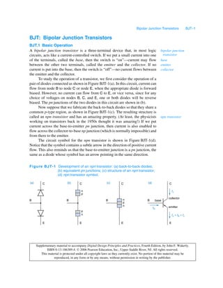
  • 1. Bipolar Junction Transistors BJT–1 BJT: Bipolar Junction Transistors BJT.1 Basic Operation A bipolar junction transistor is a three-terminal device that, in most logic bipolar junction circuits, acts like a current-controlled switch. If we put a small current into one transistor of the terminals, called the base, then the switch is “on”—current may flow base between the other two terminals, called the emitter and the collector. If no emitter current is put into the base, then the switch is “off”—no current flows between collector the emitter and the collector. To study the operation of a transistor, we first consider the operation of a pair of diodes connected as shown in Figure BJT-1(a). In this circuit, current can flow from node B to node C or node E, when the appropriate diode is forward biased. However, no current can flow from C to E, or vice versa, since for any choice of voltages on nodes B, C, and E, one or both diodes will be reverse biased. The pn junctions of the two diodes in this circuit are shown in (b). Now suppose that we fabricate the back-to-back diodes so that they share a common p-type region, as shown in Figure BJT-1(c). The resulting structure is called an npn transistor and has an amazing property. (At least, the physicists npn transistor working on transistors back in the 1950s thought it was amazing!) If we put current across the base-to-emitter pn junction, then current is also enabled to flow across the collector-to-base np junction (which is normally impossible) and from there to the emitter. The circuit symbol for the npn transistor is shown in Figure BJT-1(d). Notice that the symbol contains a subtle arrow in the direction of positive current flow. This also reminds us that the base-to-emitter junction is a pn junction, the same as a diode whose symbol has an arrow pointing in the same direction. Fig ur e BJ T-1 Development of an npn transistor: (a) back-to-back diodes; (b) equivalent pn junctions; (c) structure of an npn transistor; (d) npn transistor symbol. (a) C (b) C (c) C (d) C n Ic p collector B B B n B base p n emitter Ib p n Ie = Ib + Ic E E E E Supplementary material to accompany Digital Design Principles and Practices, Fourth Edition, by John F. Wakerly. ISBN 0-13-186389-4.  2006 Pearson Education, Inc., Upper Saddle River, NJ. All rights reserved. This material is protected under all copyright laws as they currently exist. No portion of this material may be reproduced, in any form or by any means, without permission in writing by the publisher.
  • 2. Bipolar Junction Transistors BJT–2 (a) E (b) E Ie = Ib + Ic p emitter B B base n p Fi gur e BJ T-2 Ib collector A pnp transistor: Ic (a) structure; (b) symbol. C C It is also possible to fabricate a pnp transistor, as shown in Figure BJT-2. pnp transistor However, pnp transistors are seldom used in digital circuits, so we won’t discuss them any further. The current Ie flowing out of the emitter of an npn transistor is the sum of the currents Ib and Ic flowing into the base and the collector. A transistor is often used as a signal amplifier, because over a certain operating range (the active amplifier region) the collector current is equal to a fixed constant times the base current active region (Ic = β ⋅ Ib). However, in digital circuits, we normally use a transistor as a simple switch that’s always fully “on” or fully “off,” as explained next. Figure BJT-3 shows the common-emitter configuration of an npn transis- common-emitter tor, which is most often used in digital switching applications. This configuration configuration uses two discrete resistors, R1 and R2, in addition to a single npn transistor. In this circuit, if VIN is 0 or negative, then the base-to-emitter diode junction is reverse biased, and no base current (Ib) can flow. If no base current flows, then no collector current (Ic) can flow, and the transistor is said to be cut cut off (OFF) off (OFF). VCC Fi gur e BJ T-3 Common-emitter R2 configuration of an npn transistor. Ic + R1 VIN VCE + Ib − VBE − Ie = Ib + Ic Supplementary material to accompany Digital Design Principles and Practices, Fourth Edition, by John F. Wakerly. ISBN 0-13-186389-4.  2006 Pearson Education, Inc., Upper Saddle River, NJ. All rights reserved. This material is protected under all copyright laws as they currently exist. No portion of this material may be reproduced, in any form or by any means, without permission in writing by the publisher.
  • 3. Bipolar Junction Transistors BJT–3 Since the base-to-emitter junction is a real diode, as opposed to an ideal one, VIN must reach at least +0.6 V (one diode-drop) before any base current can flow. Once this happens, Ohm’s law tells us that I b = ( V IN – 0.6 ) / R1 (We ignore the forward resistance Rf of the forward-biased base-to-emitter junction, which is usually small compared to the base resistor R1.) When base current flows, then collector current can flow in an amount proportional to Ib, that is, Ic = β ⋅ Ib The constant of proportionality, β, is called the gain of the transistor, and is in β the range of 10 to 100 for typical transistors. gain Although the base current Ib controls the collector current flow Ic , it also indirectly controls the voltage VCE across the collector-to-emitter junction, since VCE is just the supply voltage VCC minus the voltage drop across resistor R2: V CE = V CC – I c ⋅ R2 = V CC – β ⋅ I b ⋅ R2 = V CC – β ⋅ ( V IN – 0.6 ) ⋅ R2 / R1 However, in an ideal transistor VCE can never be less than zero (the transis- tor cannot just create a negative potential), and in a real transistor VCE can never be less than VCE(sat), a transistor parameter that is typically about 0.2 V. If the values of VIN, β, R1, and R2 are such that the above equation predicts a value of VCE that is less than VCE(sat), then the transistor cannot be operating in the active region and the equation does not apply. Instead, the transistor is operating in the saturation region, and is said to be saturated (ON). No matter saturation region how much current Ib we put into the base, VCE cannot drop below VCE(sat), and saturated (ON) the collector current Ic is determined mainly by the load resistor R2: I c = ( V CC – V CE(sat) ) / ( R2 + R CE(sat) ) Here, RCE(sat) is the saturation resistance of the transistor. Typically, RCE(sat) is saturation resistance 50 Ω or less and is insignificant compared with R2. Computer scientists might like to imagine an npn transistor as a device that transistor simulation continuously looks at its environment and executes the program in Table BJT-1 on the next page.. Supplementary material to accompany Digital Design Principles and Practices, Fourth Edition, by John F. Wakerly. ISBN 0-13-186389-4.  2006 Pearson Education, Inc., Upper Saddle River, NJ. All rights reserved. This material is protected under all copyright laws as they currently exist. No portion of this material may be reproduced, in any form or by any means, without permission in writing by the publisher.
  • 4. Bipolar Junction Transistors BJT–4 T ab le B JT- 1 A C program that simulates the function of an npn transistor in the common-emitter configuration. /* Transistor parameters */ #define DIODEDROP 0.6 /* volts */ #define BETA 10 #define VCE_SAT 0.2 /* volts */ #define RCE_SAT 50 /* ohms */ main() { float Vcc, Vin, R1, R2; /* circuit parameters */ float Ib, Ic, Vce; /* circuit conditions */ if (Vin < DIODEDROP) { /* cut off */ Ib = 0.0; Ic = 0.0; Vce = Vcc; } else { /* active or saturated */ Ib = (Vin - DIODEDROP) / R1; if ((Vcc - ((BETA * Ib) * R2)) >= VCE_SAT) { /* active */ Ic = BETA * Ib; Vce = Vcc - (Ic * R2); } else { /* saturated */ Vce = VCE_SAT; Ic = (Vcc - Vce) / (R2 + RCE_SAT); } } } Supplementary material to accompany Digital Design Principles and Practices, Fourth Edition, by John F. Wakerly. ISBN 0-13-186389-4.  2006 Pearson Education, Inc., Upper Saddle River, NJ. All rights reserved. This material is protected under all copyright laws as they currently exist. No portion of this material may be reproduced, in any form or by any means, without permission in writing by the publisher.
  • 5. Bipolar Junction Transistors BJT–5 VCC (a) (b) (c) VOUT IN OUT R2 VCC VOUT R1 VIN Q1 VCE(sat) VIN LOW undefined HIGH Fig ur e BJ T-4 Transistor inverter: (a) logic symbol; (b) circuit diagram; (c) transfer characteristic. BJT.2 Transistor Logic Inverter Figure BJT-4 shows that we can make a logic inverter from an npn transistor in the common-emitter configuration. When the input voltage is LOW, the output voltage is HIGH, and vice versa. In digital switching applications, bipolar transistors are often operated so they are always either cut off or saturated. That is, digital circuits such as the inverter in Figure BJT-4 are designed so that their transistors are always (well, almost always) in one of the states depicted in Figure BJT-5. When the input voltage VIN is LOW, it is low enough that Ib is zero and the transistor is cut off; the collector-emitter junction looks like an open circuit. When VIN is HIGH, Fig ur e BJ T-5 Normal states of an npn transistor in a digital switching circuit: (a) transistor symbol and currents; (b) equivalent circuit for a cut-off (OFF) transistor; (c) equivalent circuit for a saturated (ON) transistor. (a) C (b) C (c) C Ic Ic = 0 Ic > 0 B B B RCE(sat) Ib + Ib = 0 + Ib > 0 VCE(sat) = 0.2 V Ie = Ib + Ic VBE < 0.6 V Ie = 0 VBE = 0.6 V Ie = Ib + Ic − − E E E Supplementary material to accompany Digital Design Principles and Practices, Fourth Edition, by John F. Wakerly. ISBN 0-13-186389-4.  2006 Pearson Education, Inc., Upper Saddle River, NJ. All rights reserved. This material is protected under all copyright laws as they currently exist. No portion of this material may be reproduced, in any form or by any means, without permission in writing by the publisher.
  • 6. Bipolar Junction Transistors BJT–6 VCC = +5 V R VOUT VIN Switch is closed when VIN is HIGH. RCEsat Fi gur e BJ T-6 < 50 Ω Switch model for a VCEsat transistor inverter. ≈ 0.2 V it is high enough (and R1 is low enough and β is high enough) that the transistor will be saturated for any reasonable value of R2; the collector-emitter junction looks almost like a short circuit. Input voltages in the undefined region between LOW and HIGH are not normally encountered, except during transitions. This undefined region corresponds to the noise margin that we discussed with Figure 1-2 on page 8. Another way to visualize the operation of a transistor inverter is shown in Figure BJT-6. When VIN is HIGH, the transistor switch is closed, and the output terminal is connected to ground, definitely a LOW voltage. When VIN is LOW, the transistor switch is open and the output terminal is pulled to +5 V through a resistor; the output voltage is HIGH unless the output terminal is too heavily loaded (i.e., improperly connected through a low impedance to ground). Supplementary material to accompany Digital Design Principles and Practices, Fourth Edition, by John F. Wakerly. ISBN 0-13-186389-4.  2006 Pearson Education, Inc., Upper Saddle River, NJ. All rights reserved. This material is protected under all copyright laws as they currently exist. No portion of this material may be reproduced, in any form or by any means, without permission in writing by the publisher.
  • 7. Bipolar Junction Transistors BJT–7 Schottky diode Fi gur e BJ T-7 Schottky-clamped transistor: (a) circuit; collector collector base base (b) symbol. emitter emitter (a) (b) BJT.3 Schottky Transistors When the input of a saturated transistor is changed, the output does not change immediately; it takes extra time, called storage time, to come out of saturation. storage time In fact, storage time accounts for a significant portion of the propagation delay in the original TTL logic family. Storage time can be eliminated and propagation delay can be reduced by ensuring that transistors do not saturate in normal operation. Contemporary TTL logic families do this by placing a Schottky diode between the base and collector Schottky diode of each transistor that might saturate, as shown in Figure BJT-7. The resulting Schottky-clamped transistors, which do not saturate, are called Schottky-clamped transistors or transistor Schottky transistors for short. Schottky transistor When forward biased, a Schottky diode’s voltage drop is much less than a standard diode’s, 0.25 V vs. 0.6 V. In a standard saturated transistor, the base-to- collector voltage is 0.4 V, as shown in Figure BJT-8(a). In a Schottky transistor, the Schottky diode shunts current from the base into the collector before the transistor goes into saturation, as shown in (b). Figure BJT-9 is the circuit diagram of a simple inverter using a Schottky transistor. (a) (b) + 0.25 V − − − VBC = 0.4 V Ic Ic VBC = 0.25 V + + + + VCE = 0.2 V VCE = 0.35 V Ib + − Ib + − VBE = 0.6 V VBE = 0.6 V − − Fi gur e B J T-8 Operation of a transistor with large base current: (a) standard saturated transistor; (b) transistor with Schottky diode to prevent saturation. Supplementary material to accompany Digital Design Principles and Practices, Fourth Edition, by John F. Wakerly. ISBN 0-13-186389-4.  2006 Pearson Education, Inc., Upper Saddle River, NJ. All rights reserved. This material is protected under all copyright laws as they currently exist. No portion of this material may be reproduced, in any form or by any means, without permission in writing by the publisher.
  • 8. Bipolar Junction Transistors BJT–8 VCC F igu re BJ T-9 Inverter using Schottky transistor. R2 VOUT R1 VIN Q1 Supplementary material to accompany Digital Design Principles and Practices, Fourth Edition, by John F. Wakerly. ISBN 0-13-186389-4.  2006 Pearson Education, Inc., Upper Saddle River, NJ. All rights reserved. This material is protected under all copyright laws as they currently exist. No portion of this material may be reproduced, in any form or by any means, without permission in writing by the publisher.