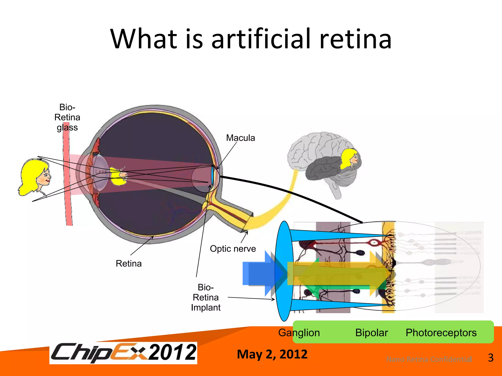
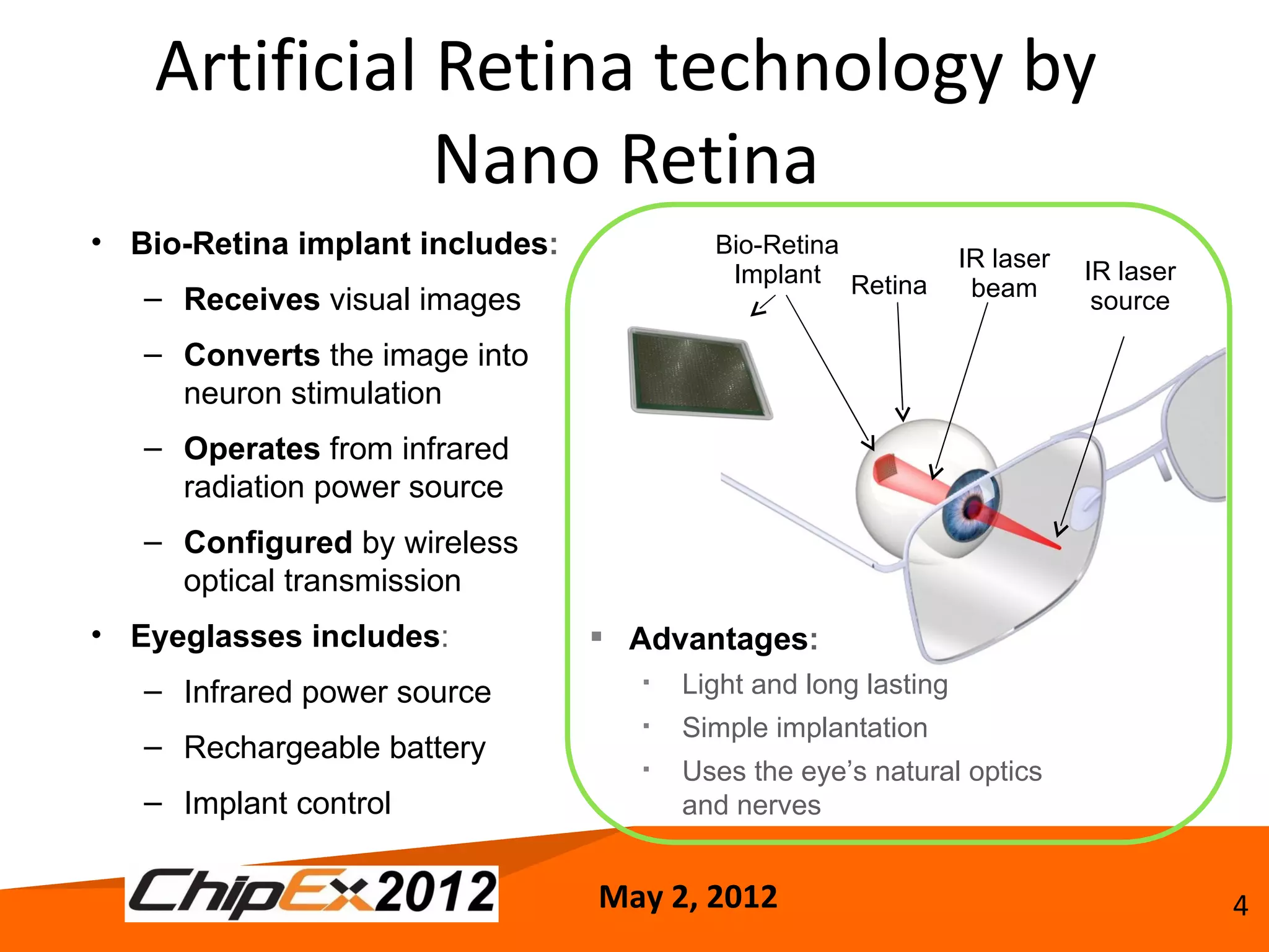
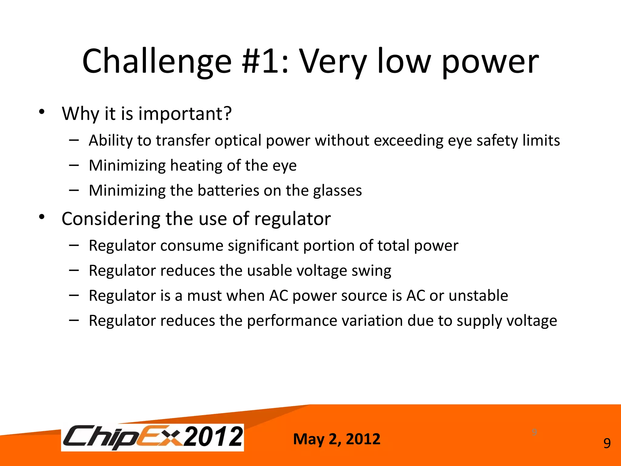
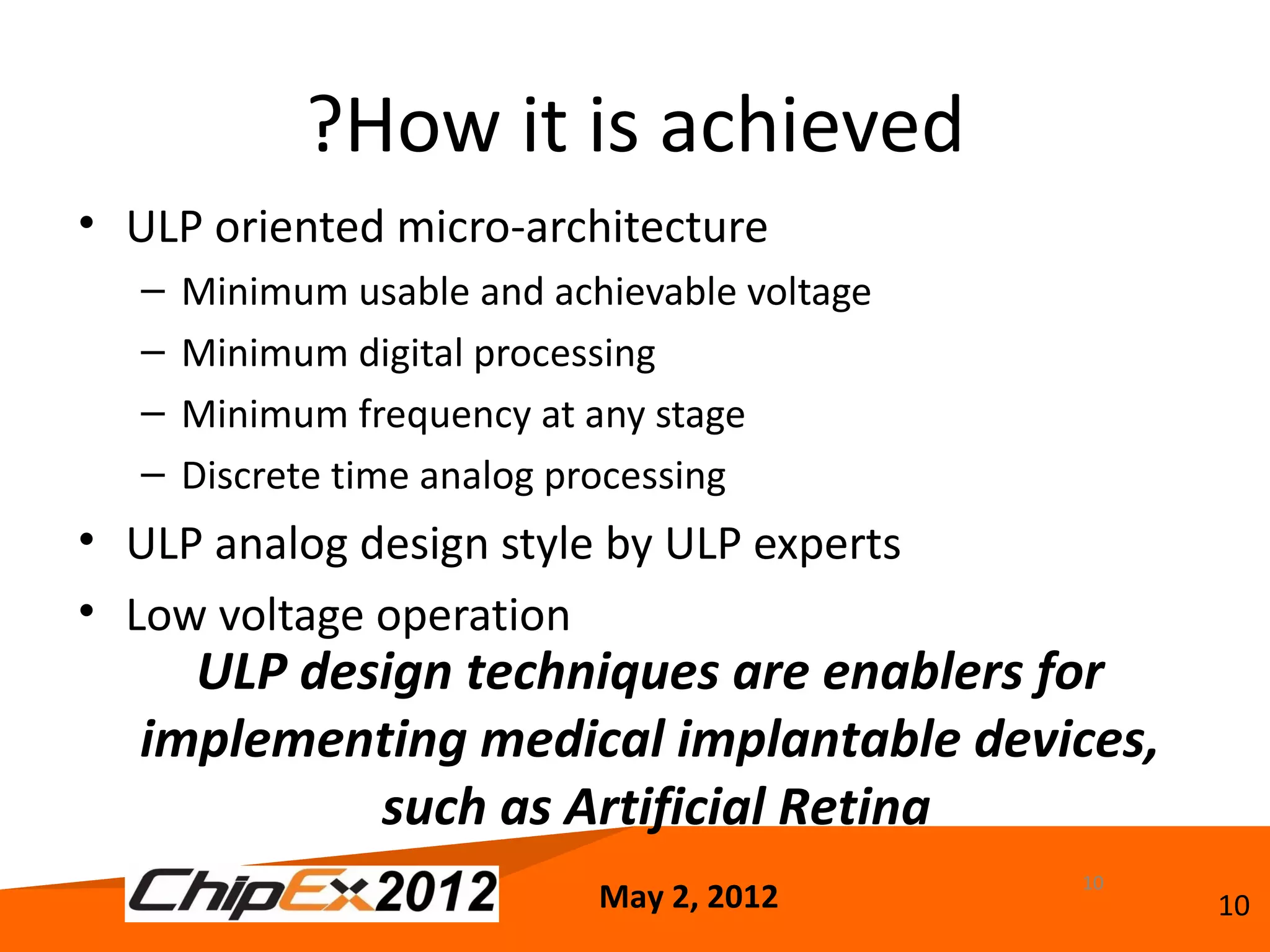
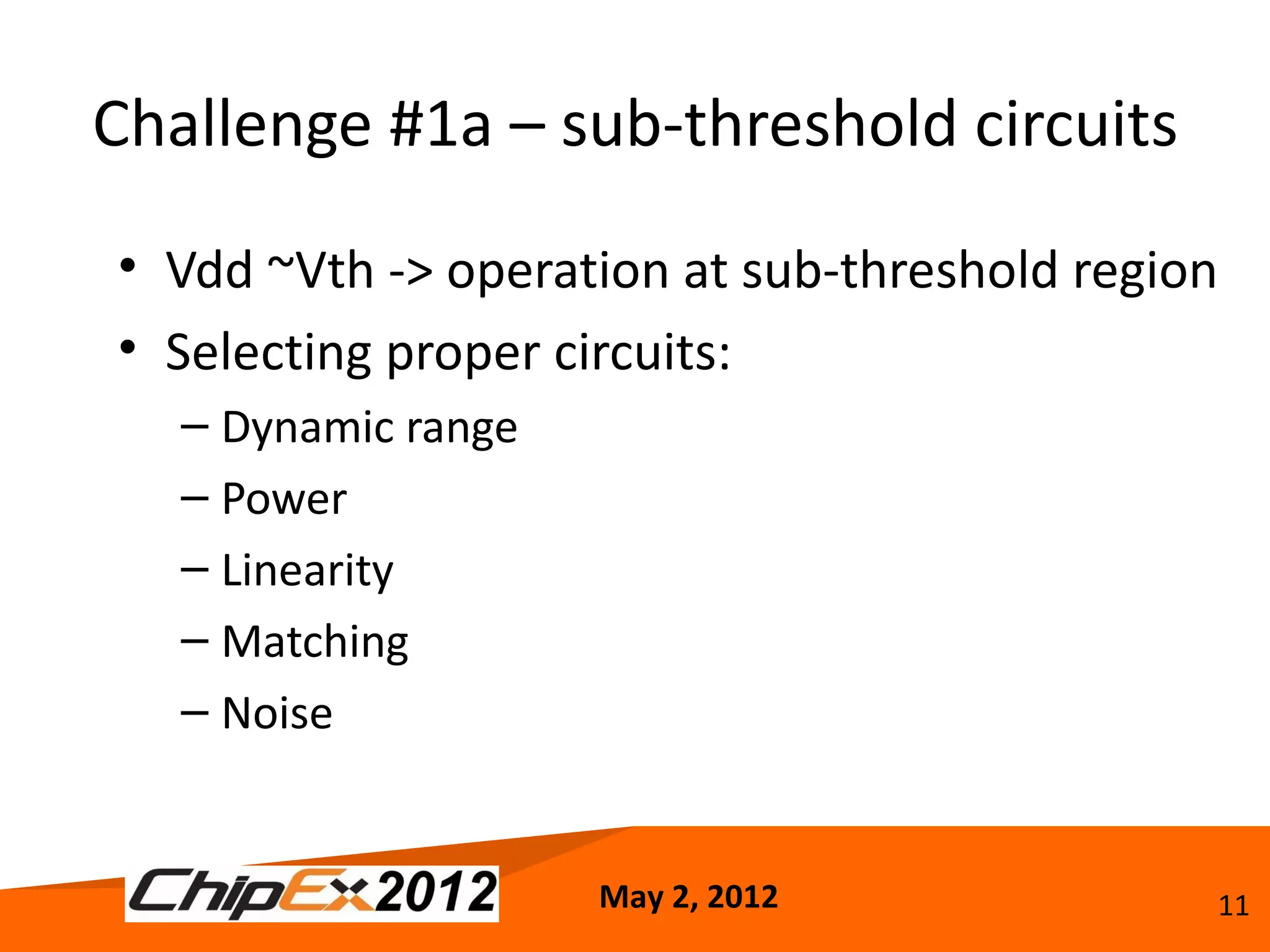
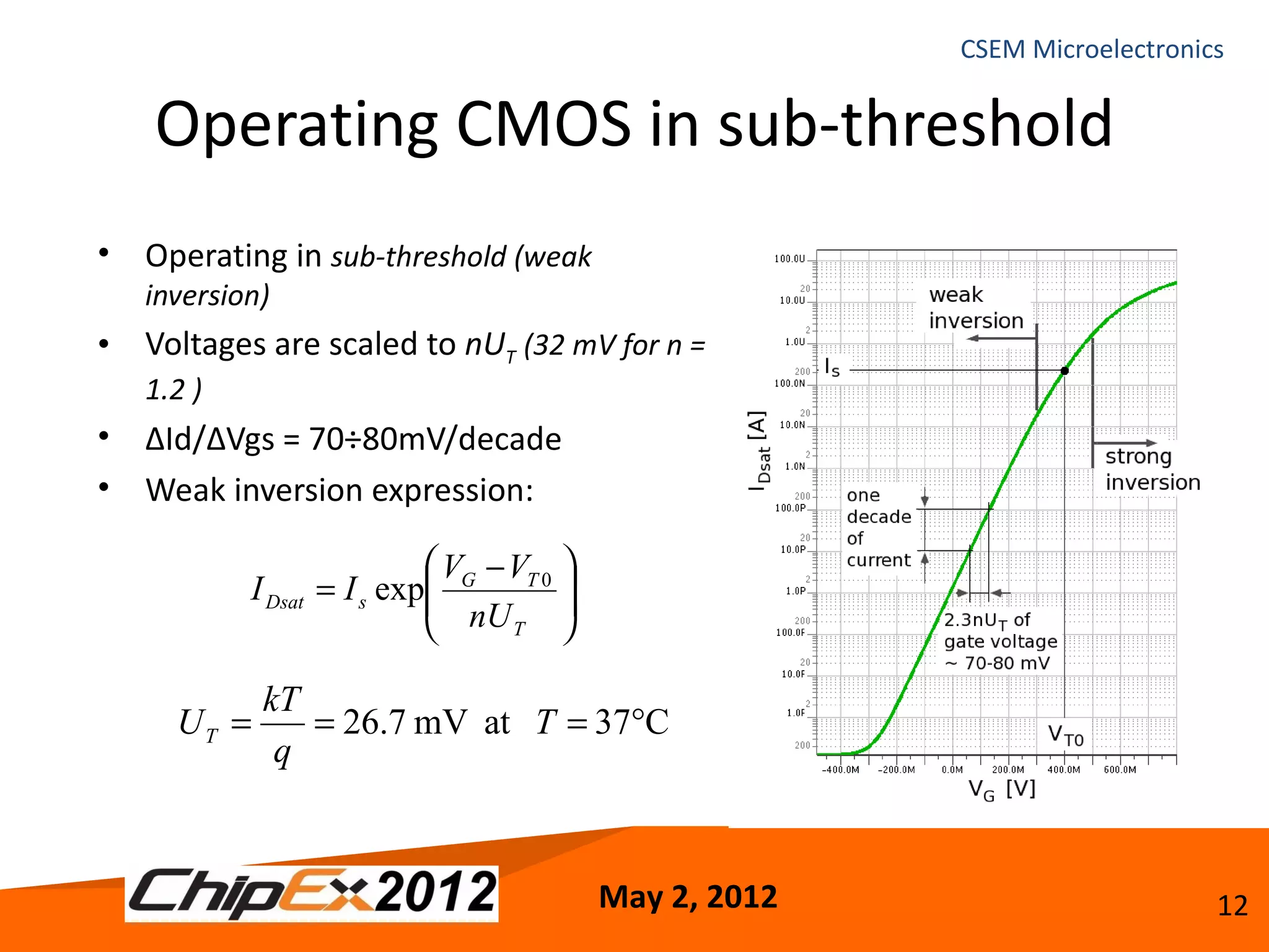
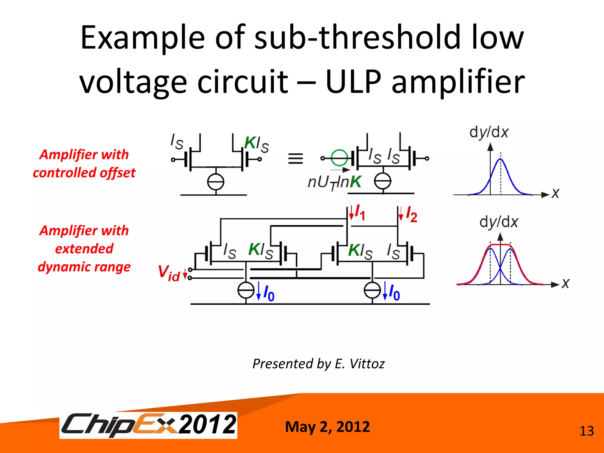
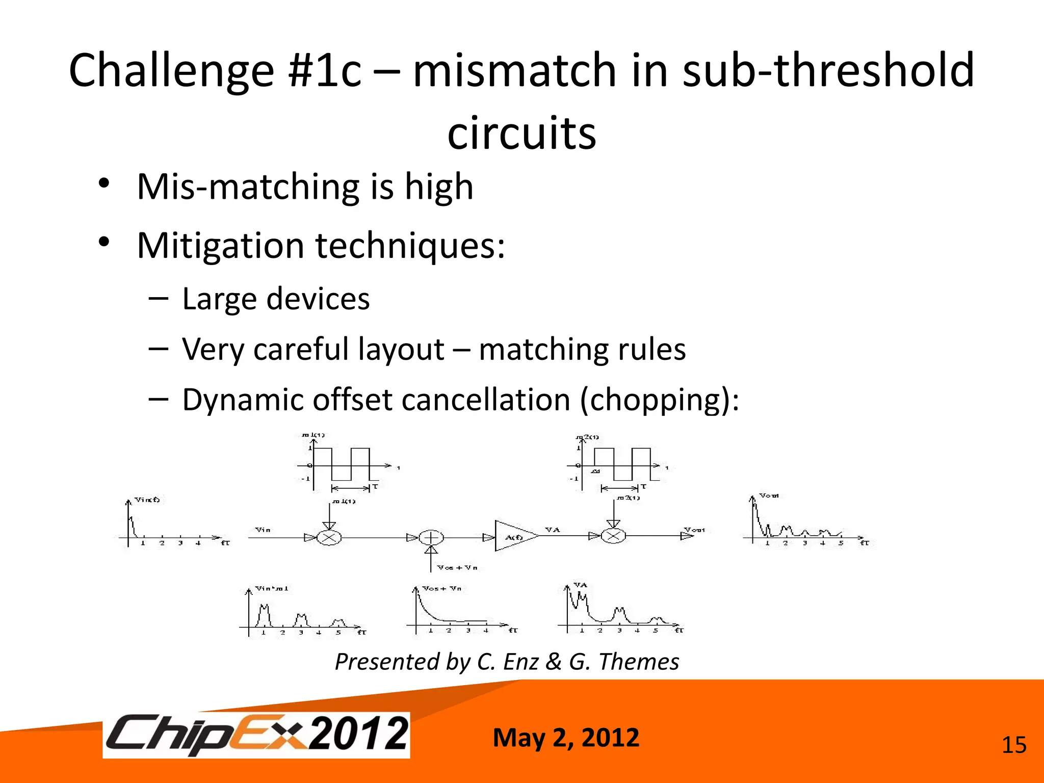
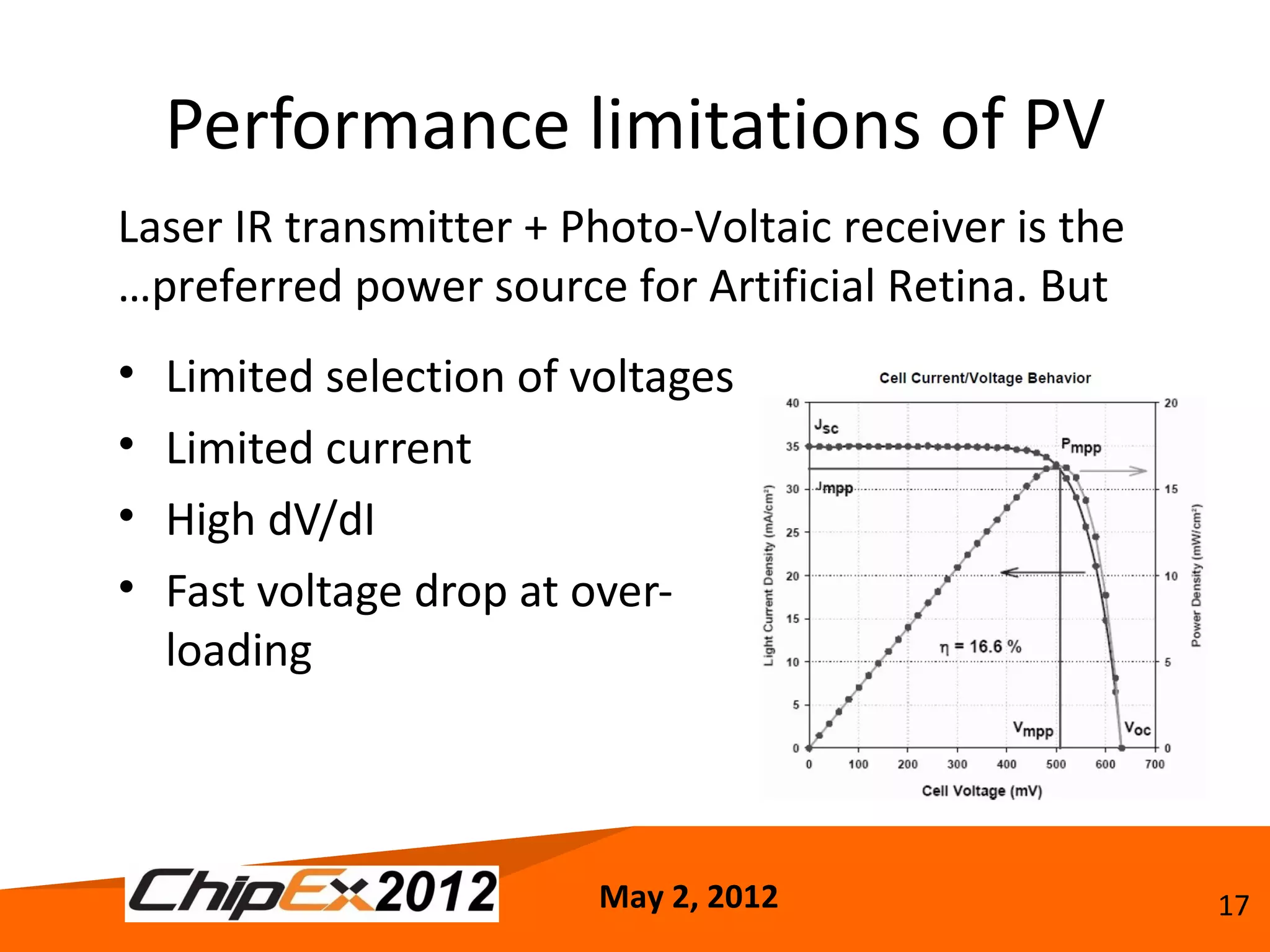
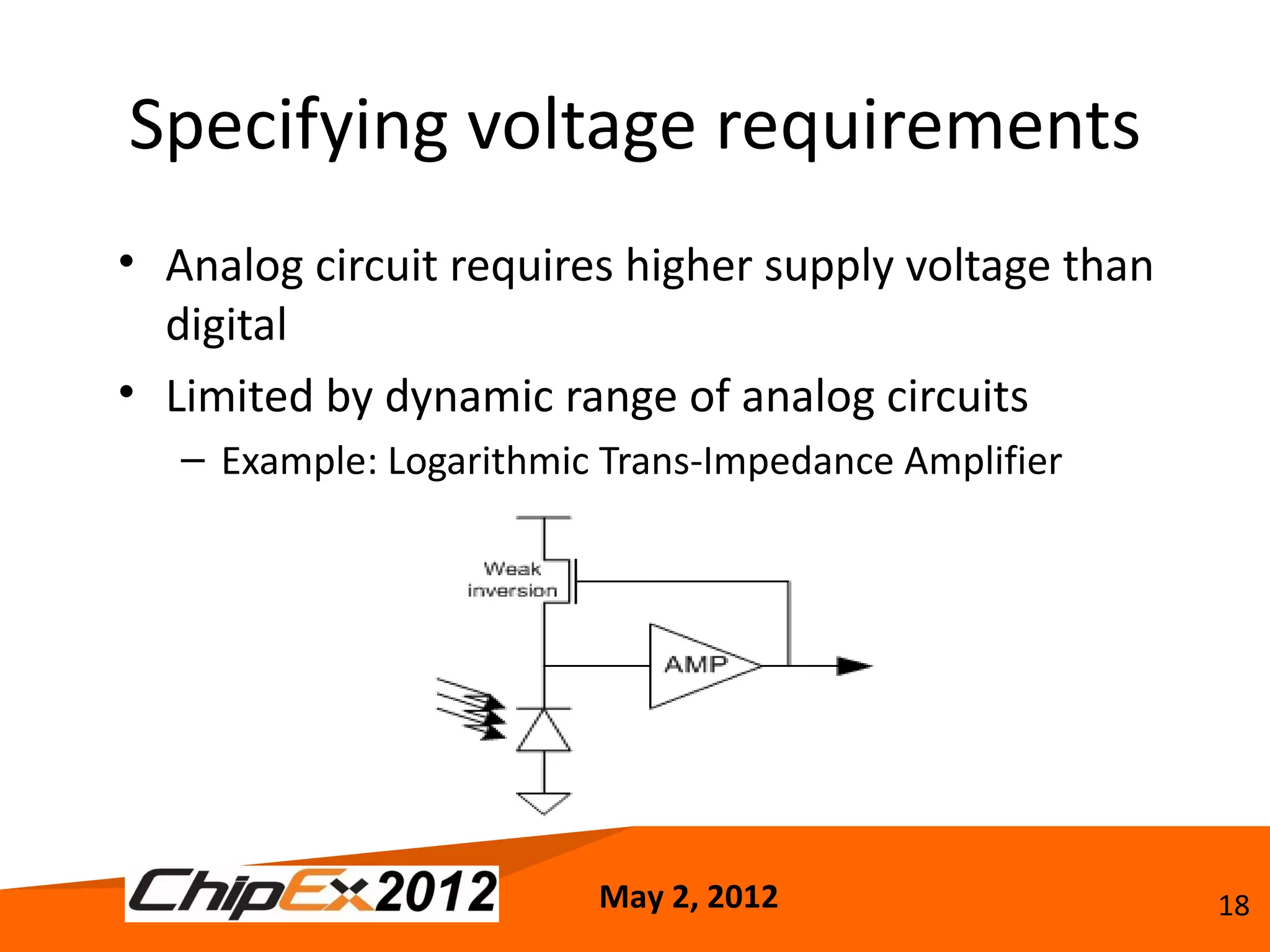
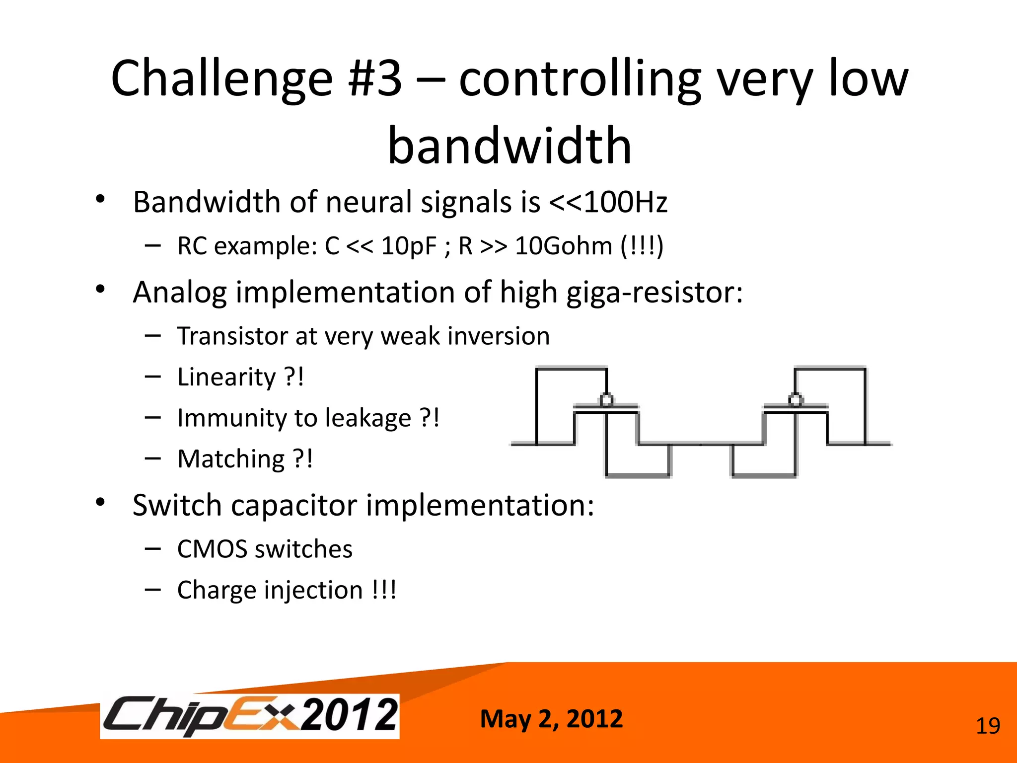
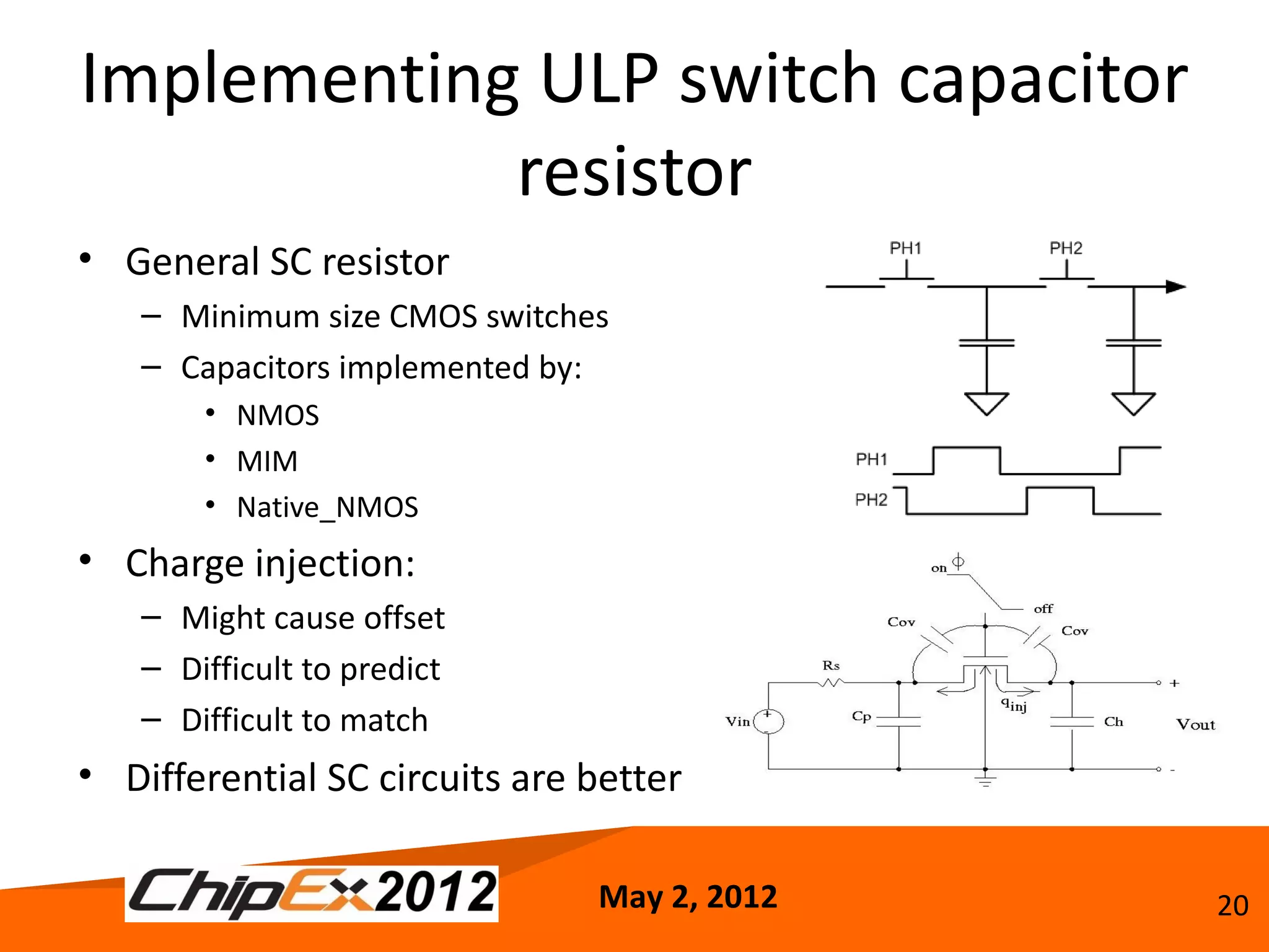
Practical issues and solutions in
Ultra Low Power design
  for Artificial Retina
             May 2, 2012

         Tuvia Liran
        Nano Retina Inc.


                May 2, 2012          1
Outline
•   What is Artificial Retina
•   Key technical challenges
•   Micro-architecture of Artificial Retina
•   Challenge #1 – power reduction
•   Challenge #2 – selection of supply source
•   Challenge #3 – controlling very low bandwidth
•   Summary


                           May 2, 2012              2
What is artificial retina
                              Vision Pathway with Bio-Retina

 Bio-
Retina
glass
                            Macula


                      Optic nerve
         Retina

                    Bio-
                   Retina
                  Implant

                                     Ganglion    Bipolar    Photoreceptors

                              May 2, 2012              Nano Retina Confidential
                                                                              3   3
Artificial Retina technology by
               Nano Retina
• Bio-Retina implant includes:           Bio-Retina
                                                                IR laser
                                          Implant Retina                   IR laser
   – Receives visual images                                      beam       source

   – Converts the image into
     neuron stimulation
   – Operates from infrared
     radiation power source
   – Configured by wireless
     optical transmission
• Eyeglasses includes:            Advantages:
   – Infrared power source            Light and long lasting
                                      Simple implantation
   – Rechargeable battery
                                      Uses the eye’s natural optics
   – Implant control                   and nerves


                                 May 2, 2012                                          4
Nano Retina technology


                         5
         May 2, 2012         5
Key technical challenges
•   Ultra low power (ULP) (<300uW)
•   Weak power source
•   Very low bandwidth (1÷40Hz)
•   Wide dynamic range (>5 decades = ~17 bits)
•   Sufficient resolution (~1000 pixels)
•   Wirelessly configurable (w/o antenna)
•   Very small device (<15mm2 including package)


                                                   6
                            May 2, 2012                6
Key development steps
• Phase 1: Providing proof of concept
   – Development of Micro-electrode array
     (MEA)
   – Defining process flow & vendors
   – Development of ULP test chip
   – Performing pre-clinical experiments
• Phase 2: Development of prototypes
   – Fully compliance for medical experiments
   – Full functionality
   – Complementary accessories


                                May 2, 2012     7
Micro architecture of Artificial Retina
    • Process: TSL018 CIS      • MEA: by NR
    • Power: GaAs PV           • Design: CSEM


8                           May 2, 2012         8
Challenge #1: Very low power
• Why it is important?
   – Ability to transfer optical power without exceeding eye safety limits
   – Minimizing heating of the eye
   – Minimizing the batteries on the glasses
• Considering the use of regulator
   –   Regulator consume significant portion of total power
   –   Regulator reduces the usable voltage swing
   –   Regulator is a must when AC power source is AC or unstable
   –   Regulator reduces the performance variation due to supply voltage


                                                                     9
                                   May 2, 2012                               9
?How it is achieved
• ULP oriented micro-architecture
   –   Minimum usable and achievable voltage
   –   Minimum digital processing
   –   Minimum frequency at any stage
   –   Discrete time analog processing
• ULP analog design style by ULP experts
• Low voltage operation
     ULP design techniques are enablers for
   implementing medical implantable devices,
            such as Artificial Retina
                                               10
                             May 2, 2012            10
Challenge #1a – sub-threshold circuits
• Vdd ~Vth -> operation at sub-threshold region
• Selecting proper circuits:
   – Dynamic range
   – Power
   – Linearity
   – Matching
   – Noise


                     May 2, 2012              11
CSEM Microelectronics


    Operating CMOS in sub-threshold
•   Operating in sub-threshold (weak
    inversion)
•   Voltages are scaled to nUT (32 mV for n =
    1.2 )
•   ∆Id/∆Vgs = 70÷80mV/decade
•   Weak inversion expression:

                               VG − VT 0 
            I Dsat   = I s exp
                               nU       
                                    T    

           kT
      UT =    = 26.7 mV at T = 37°C
            q


                                              May 2, 2012                       12
Example of sub-threshold low
       voltage circuit – ULP amplifier
 Amplifier with
controlled offset


Amplifier with
  extended
dynamic range


                    Presented by E. Vittoz


                         May 2, 2012         13
Challenge #1b – device modeling
• Conventional BSIM3/4 are not accurate at sub-
  threshold
• EKV models are more accurate (availability ?!)
• Need also accurate models for monte-carlo & noise


                      May 2, 2012                     14
Challenge #1c – mismatch in sub-threshold
                 circuits
 • Mis-matching is high
 • Mitigation techniques:
    – Large devices
    – Very careful layout – matching rules
    – Dynamic offset cancellation (chopping):


                Presented by C. Enz & G. Themes

                              May 2, 2012         15
Challenge #2 – Selection of power source
• Relevant power sources:
  – Battery
  – Energy harvesting
  – Electromagnetic power
  – Optical power transfer


                     May 2, 2012           16
Performance limitations of PV
Laser IR transmitter + Photo-Voltaic receiver is the
…preferred power source for Artificial Retina. But
•   Limited selection of voltages
•   Limited current
•   High dV/dI
•   Fast voltage drop at over-
    loading


                          May 2, 2012                  17
Specifying voltage requirements
• Analog circuit requires higher supply voltage than
  digital
• Limited by dynamic range of analog circuits
   – Example: Logarithmic Trans-Impedance Amplifier


                         May 2, 2012                   18
Challenge #3 – controlling very low
            bandwidth
• Bandwidth of neural signals is <<100Hz
   – RC example: C << 10pF ; R >> 10Gohm (!!!)
• Analog implementation of high giga-resistor:
   –   Transistor at very weak inversion
   –   Linearity ?!
   –   Immunity to leakage ?!
   –   Matching ?!
• Switch capacitor implementation:
   – CMOS switches
   – Charge injection !!!


                                 May 2, 2012     19
Implementing ULP switch capacitor
            resistor
• General SC resistor
   – Minimum size CMOS switches
   – Capacitors implemented by:
       • NMOS
       • MIM
       • Native_NMOS
• Charge injection:
   – Might cause offset
   – Difficult to predict
   – Difficult to match
• Differential SC circuits are better

                               May 2, 2012   20
Summary
• ULP is enabling technology for implantable medical devices,
  such as Artificial Retina
• ULP implementation is challenging but doable
• Key factors for successful design:
   –   Optimal micro-architecture
   –   Optimal selection of power sourcing
   –   Know-how in sub-threshold design
   –   Availability of EKV models
   –   Intensive monte-carlo simulations


                                 May 2, 2012                    21

Practical solutions in ultra low power design for artificial retina

  • 1.
    Practical issues andsolutions in Ultra Low Power design for Artificial Retina May 2, 2012 Tuvia Liran Nano Retina Inc. May 2, 2012 1
  • 2.
    Outline • What is Artificial Retina • Key technical challenges • Micro-architecture of Artificial Retina • Challenge #1 – power reduction • Challenge #2 – selection of supply source • Challenge #3 – controlling very low bandwidth • Summary May 2, 2012 2
  • 3.
    What is artificialretina Vision Pathway with Bio-Retina Bio- Retina glass Macula Optic nerve Retina Bio- Retina Implant Ganglion Bipolar Photoreceptors May 2, 2012 Nano Retina Confidential 3 3
  • 4.
    Artificial Retina technologyby Nano Retina • Bio-Retina implant includes: Bio-Retina IR laser Implant Retina IR laser – Receives visual images beam source – Converts the image into neuron stimulation – Operates from infrared radiation power source – Configured by wireless optical transmission • Eyeglasses includes:  Advantages: – Infrared power source  Light and long lasting  Simple implantation – Rechargeable battery  Uses the eye’s natural optics – Implant control and nerves May 2, 2012 4
  • 5.
    Nano Retina technology 5 May 2, 2012 5
  • 6.
    Key technical challenges • Ultra low power (ULP) (<300uW) • Weak power source • Very low bandwidth (1÷40Hz) • Wide dynamic range (>5 decades = ~17 bits) • Sufficient resolution (~1000 pixels) • Wirelessly configurable (w/o antenna) • Very small device (<15mm2 including package) 6 May 2, 2012 6
  • 7.
    Key development steps •Phase 1: Providing proof of concept – Development of Micro-electrode array (MEA) – Defining process flow & vendors – Development of ULP test chip – Performing pre-clinical experiments • Phase 2: Development of prototypes – Fully compliance for medical experiments – Full functionality – Complementary accessories May 2, 2012 7
  • 8.
    Micro architecture ofArtificial Retina • Process: TSL018 CIS • MEA: by NR • Power: GaAs PV • Design: CSEM 8 May 2, 2012 8
  • 9.
    Challenge #1: Verylow power • Why it is important? – Ability to transfer optical power without exceeding eye safety limits – Minimizing heating of the eye – Minimizing the batteries on the glasses • Considering the use of regulator – Regulator consume significant portion of total power – Regulator reduces the usable voltage swing – Regulator is a must when AC power source is AC or unstable – Regulator reduces the performance variation due to supply voltage 9 May 2, 2012 9
  • 10.
    ?How it isachieved • ULP oriented micro-architecture – Minimum usable and achievable voltage – Minimum digital processing – Minimum frequency at any stage – Discrete time analog processing • ULP analog design style by ULP experts • Low voltage operation ULP design techniques are enablers for implementing medical implantable devices, such as Artificial Retina 10 May 2, 2012 10
  • 11.
    Challenge #1a –sub-threshold circuits • Vdd ~Vth -> operation at sub-threshold region • Selecting proper circuits: – Dynamic range – Power – Linearity – Matching – Noise May 2, 2012 11
  • 12.
    CSEM Microelectronics Operating CMOS in sub-threshold • Operating in sub-threshold (weak inversion) • Voltages are scaled to nUT (32 mV for n = 1.2 ) • ∆Id/∆Vgs = 70÷80mV/decade • Weak inversion expression:  VG − VT 0  I Dsat = I s exp  nU    T  kT UT = = 26.7 mV at T = 37°C q May 2, 2012 12
  • 13.
    Example of sub-thresholdlow voltage circuit – ULP amplifier Amplifier with controlled offset Amplifier with extended dynamic range Presented by E. Vittoz May 2, 2012 13
  • 14.
    Challenge #1b –device modeling • Conventional BSIM3/4 are not accurate at sub- threshold • EKV models are more accurate (availability ?!) • Need also accurate models for monte-carlo & noise May 2, 2012 14
  • 15.
    Challenge #1c –mismatch in sub-threshold circuits • Mis-matching is high • Mitigation techniques: – Large devices – Very careful layout – matching rules – Dynamic offset cancellation (chopping): Presented by C. Enz & G. Themes May 2, 2012 15
  • 16.
    Challenge #2 –Selection of power source • Relevant power sources: – Battery – Energy harvesting – Electromagnetic power – Optical power transfer May 2, 2012 16
  • 17.
    Performance limitations ofPV Laser IR transmitter + Photo-Voltaic receiver is the …preferred power source for Artificial Retina. But • Limited selection of voltages • Limited current • High dV/dI • Fast voltage drop at over- loading May 2, 2012 17
  • 18.
    Specifying voltage requirements •Analog circuit requires higher supply voltage than digital • Limited by dynamic range of analog circuits – Example: Logarithmic Trans-Impedance Amplifier May 2, 2012 18
  • 19.
    Challenge #3 –controlling very low bandwidth • Bandwidth of neural signals is <<100Hz – RC example: C << 10pF ; R >> 10Gohm (!!!) • Analog implementation of high giga-resistor: – Transistor at very weak inversion – Linearity ?! – Immunity to leakage ?! – Matching ?! • Switch capacitor implementation: – CMOS switches – Charge injection !!! May 2, 2012 19
  • 20.
    Implementing ULP switchcapacitor resistor • General SC resistor – Minimum size CMOS switches – Capacitors implemented by: • NMOS • MIM • Native_NMOS • Charge injection: – Might cause offset – Difficult to predict – Difficult to match • Differential SC circuits are better May 2, 2012 20
  • 21.
    Summary • ULP isenabling technology for implantable medical devices, such as Artificial Retina • ULP implementation is challenging but doable • Key factors for successful design: – Optimal micro-architecture – Optimal selection of power sourcing – Know-how in sub-threshold design – Availability of EKV models – Intensive monte-carlo simulations May 2, 2012 21