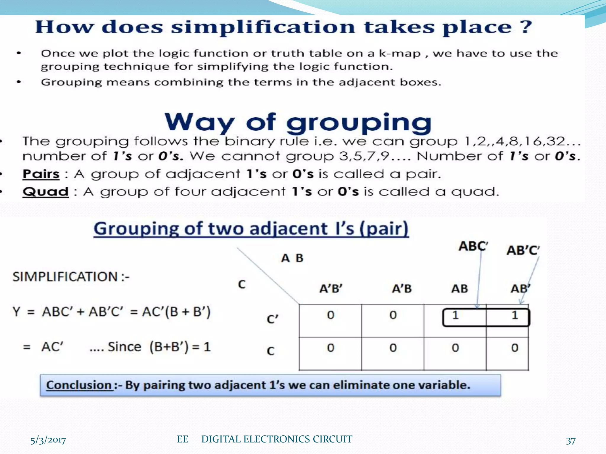
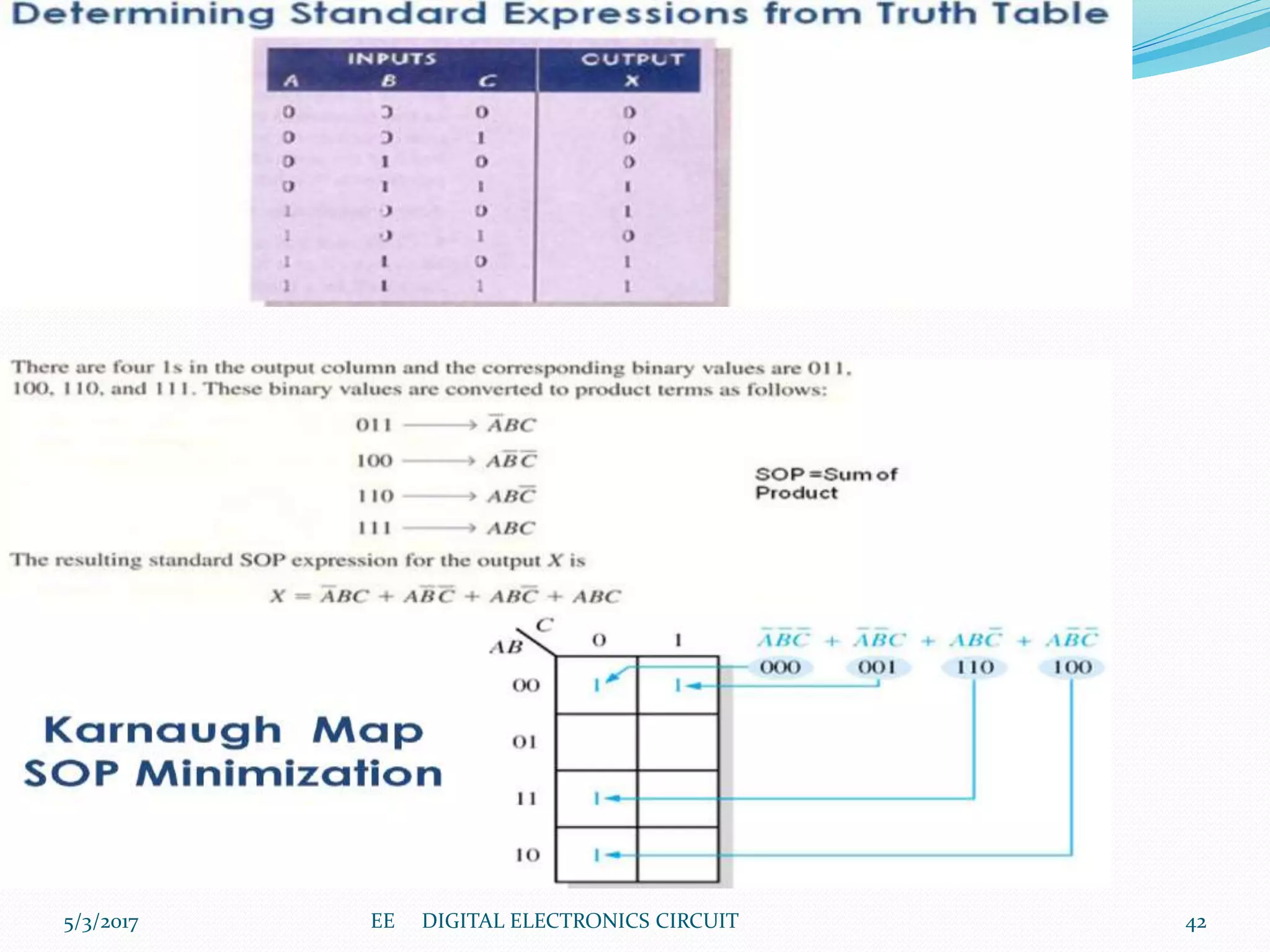
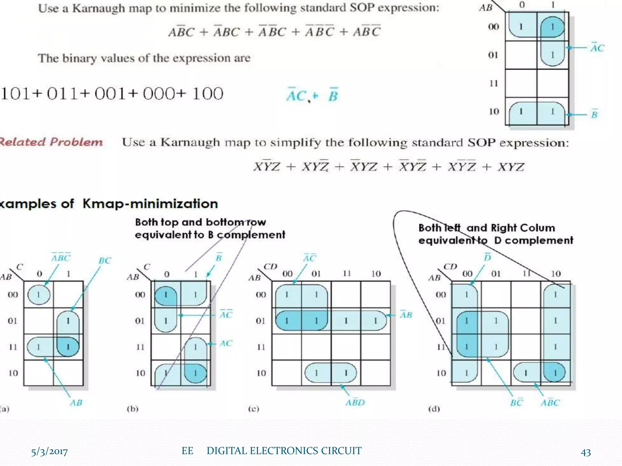
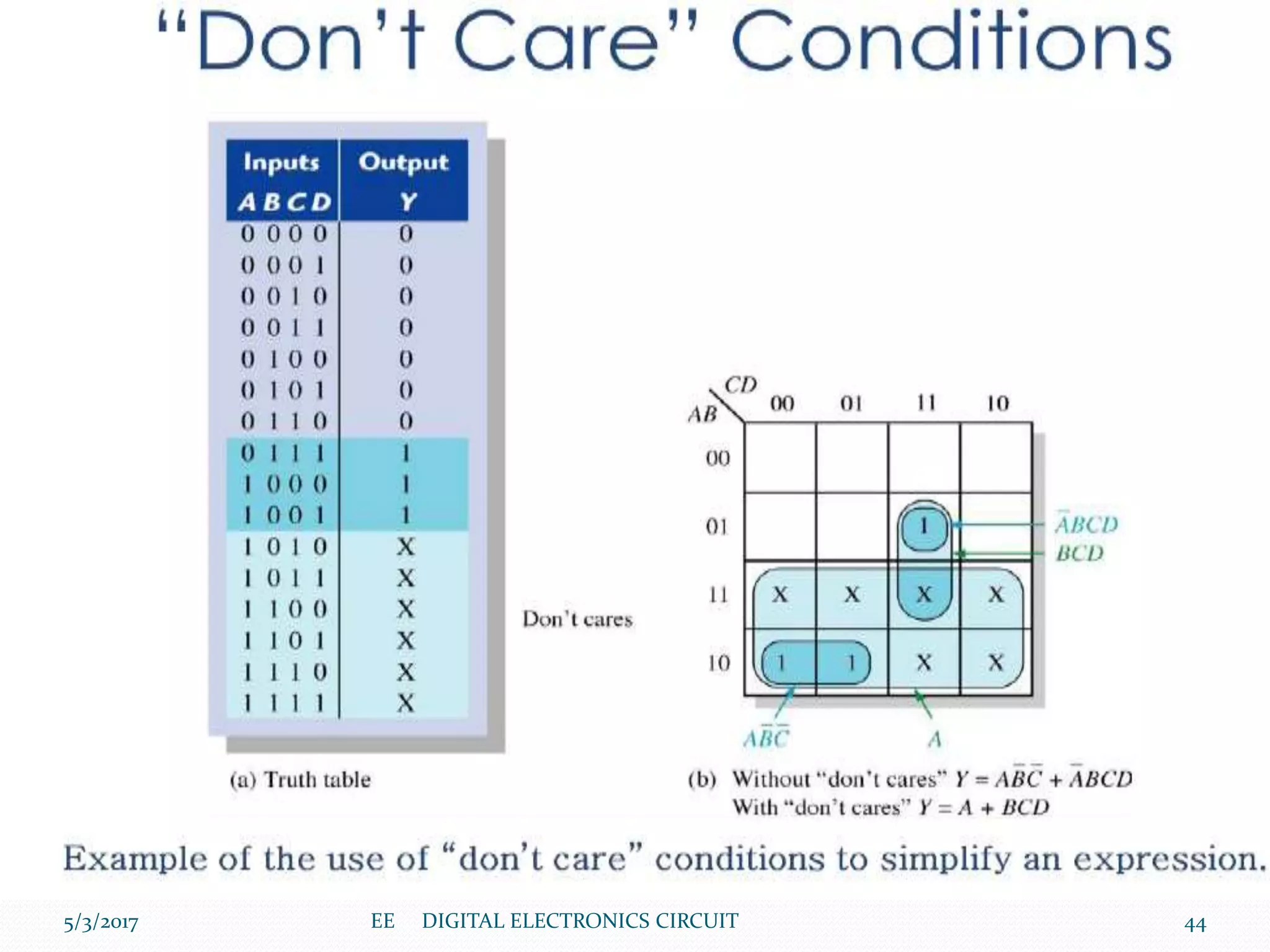
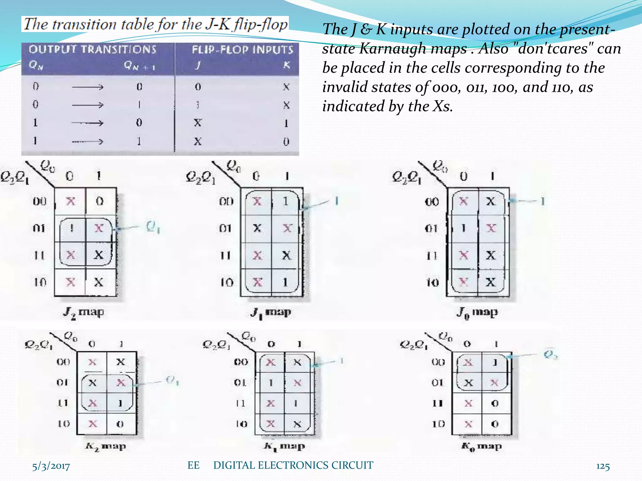
The document provides an overview of the course content for Digital Electronics Circuits. It is divided into three modules:
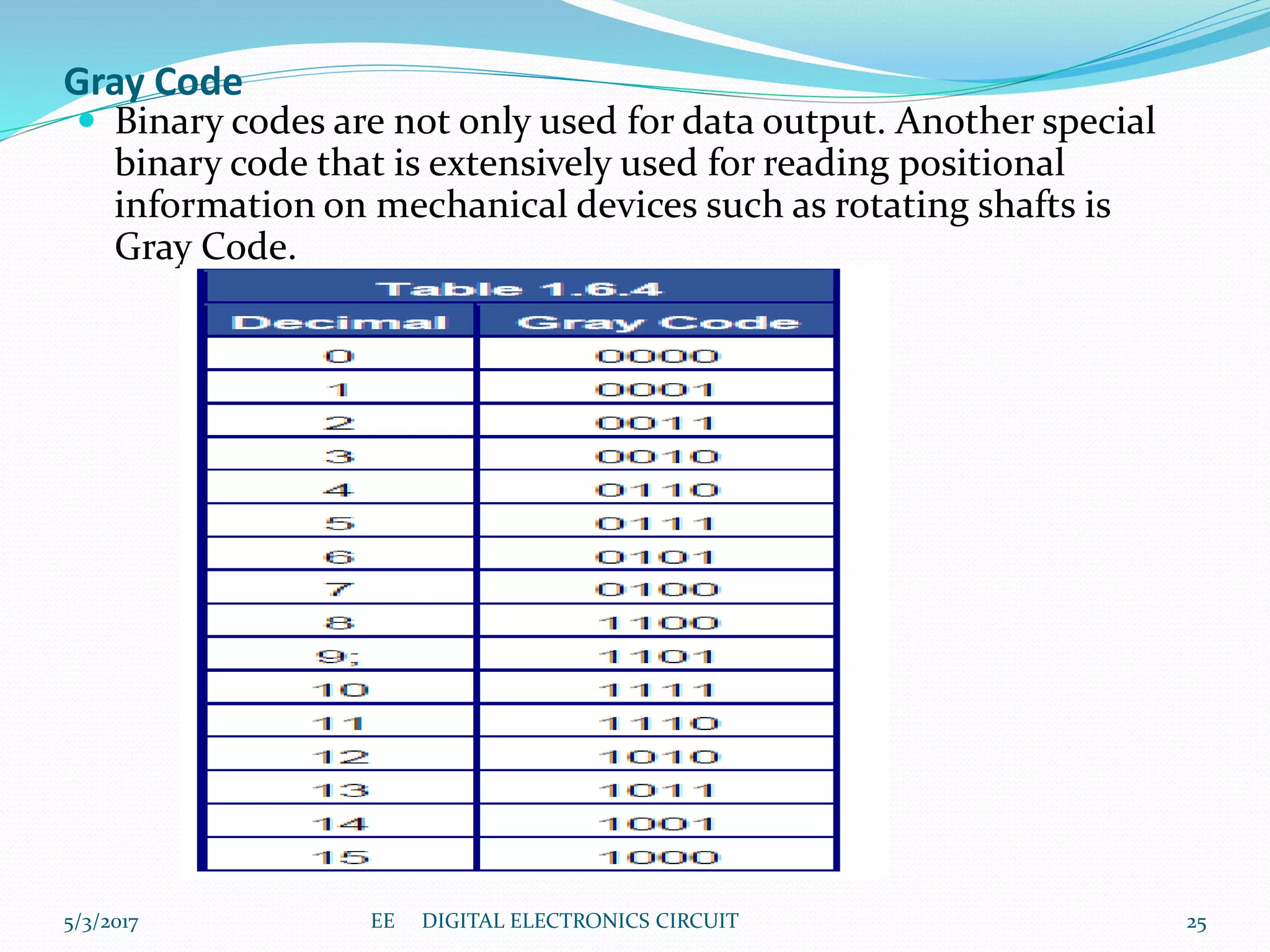
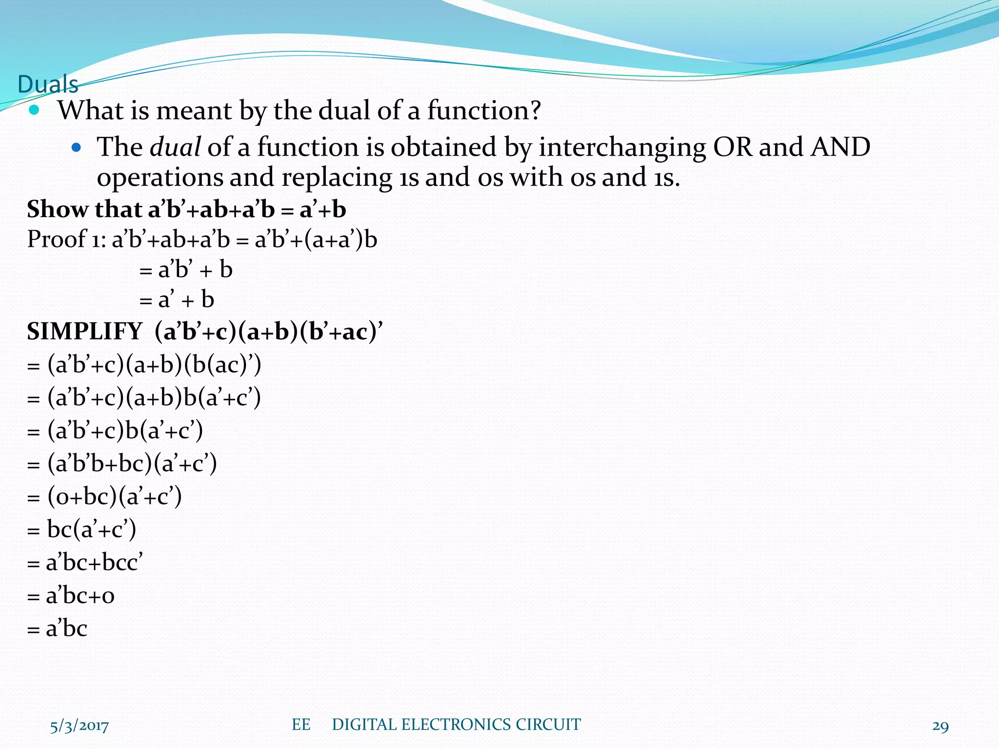
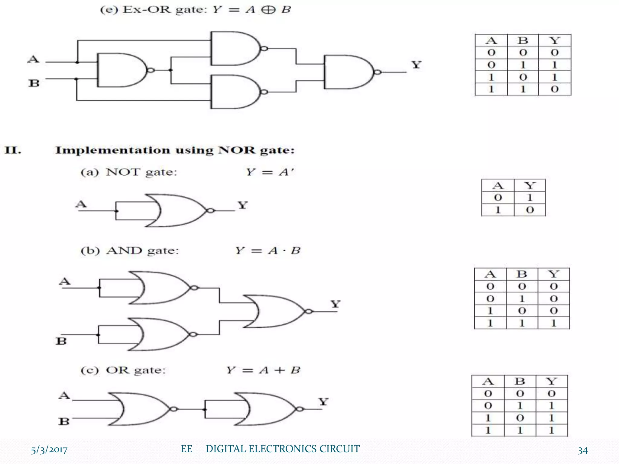
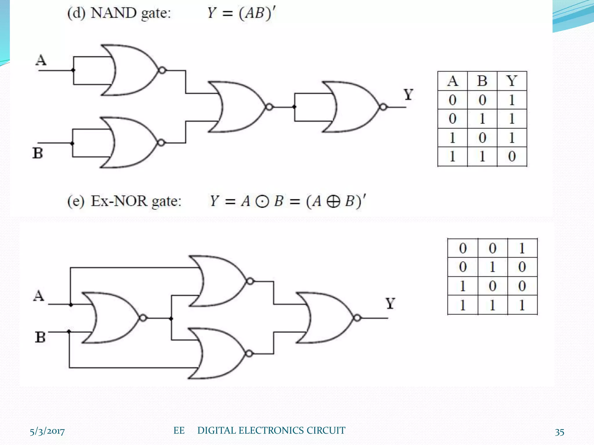
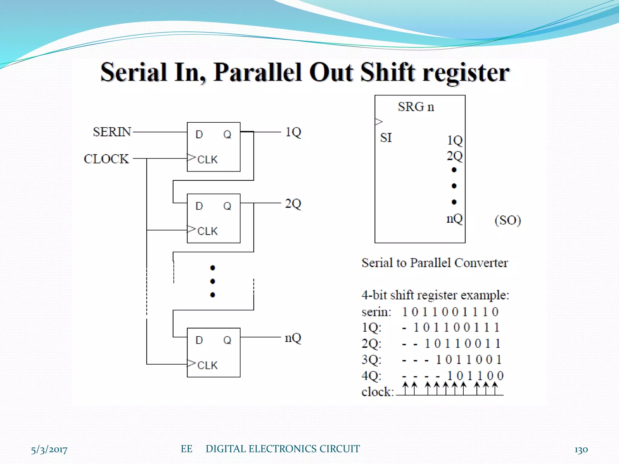
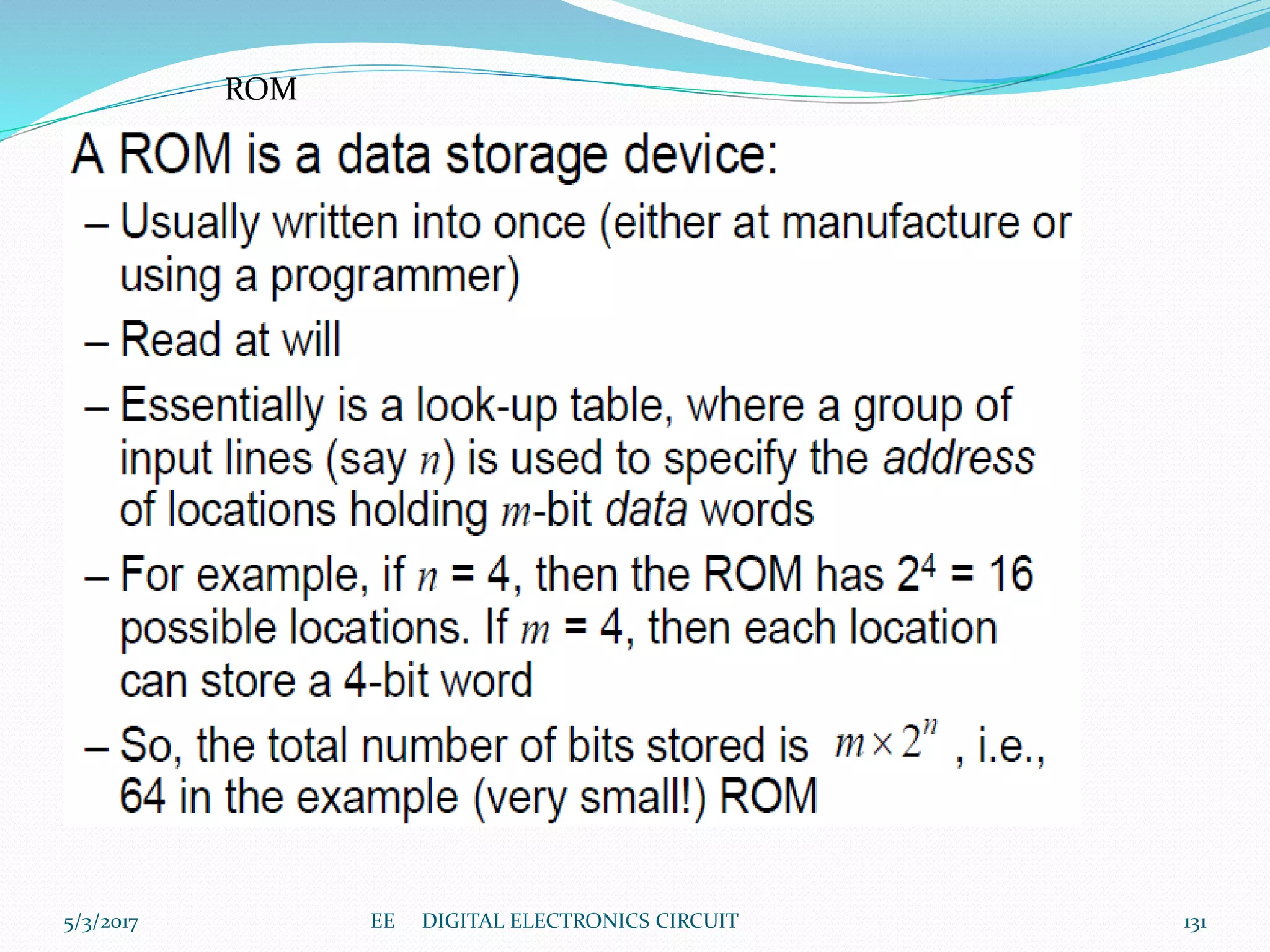
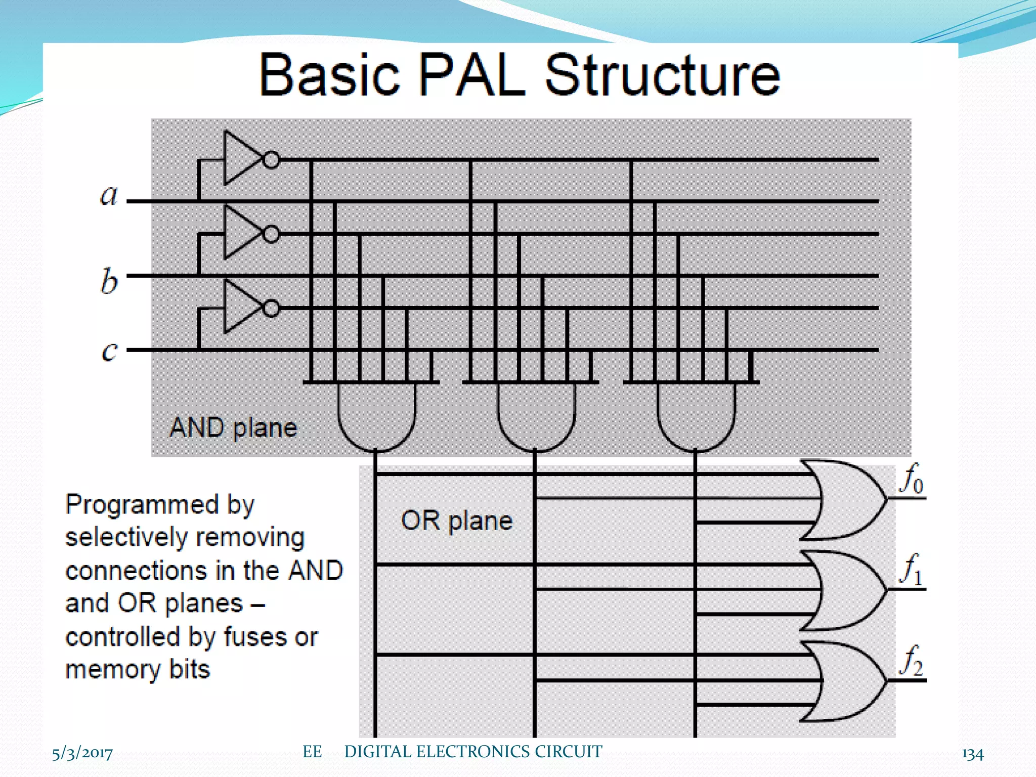
Module I covers number systems, binary codes, Boolean algebra, logic gates and truth tables. Module II focuses on combinational logic design including adders, encoders and multiplexers. Module III discusses sequential logic design, counters, shift registers, memory and programmable logic devices. The document lists common logic families and provides examples of number system conversions and Boolean logic simplifications. It is intended to outline the key topics that will be covered in the course.
Numbering system, binary number system, octal number system, decimal number system, hexadecimal number system.
Code conversion, Conversion from one number system to another, floating point numbers
Numbering system, binary number system, octal number system, decimal number system, hexadecimal number system.
Code conversion, Conversion from one number system to another, floating point numbers
BCS Certificate Level Examination. Computer and Network Technology (CNT) subject. Fundamentals of Computer Science. Data Representation in Computers. Learn about decimal, binary, octal and hexadecimal number systems and conversion between systems. Learn about binary addition and subtraction. For a complete subject coverage including Information Systems and Software Developments subjects, please visit to https://www.bcsonlinelectures.com/
To Download this click on the link below:-
http://www29.zippyshare.com/v/42478054/file.html
Number System
Decimal Number System
Binary Number System
Why Binary?
Octal Number System
Hexadecimal Number System
Relationship between Hexadecimal, Octal, Decimal, and Binary
Number Conversions
This is the second lesson of Computer and Network Technology subject of BCS HEQ Certificate Level exam.
Subject: Computer and Network Technology (CNT)
Chapter: Fundamentals
Lesson: Data Representation in Computers
This lesson discuss about how integers, floating point numbers and characters are handled by modern computers.
For more lessons please visit https://www.bcsonlinelectures.com website.
The binary number system and digital codes are fundamental to computers and to digital electronics in general. You will learn Binary addition, subtraction, multiplication, and Division.
The manual introduces the reader to the logic of arithmetic operations in computers, the logics of Boolean and Zhegalkin, the logic of decomposition, research and minimization of Boolean functions, the logic of temporal and recurrent Boolean functions, the theory of automata and regular operations, and on their basis the logic of building various computers computer circuits. Considerable attention is paid to the correct application of precise notations, definitions, simplified proof of theorems, logic and algorithms for building computer circuits.
References:
"Digital Systems Principles And Application"
Sixth Edition, Ronald J. Tocci.
"Digital Systems Fundamentals"
P.W Chandana Prasad, Lau Siong Hoe,
Dr. Ashutosh Kumar Singh, Muhammad Suryanata.
Number System
Number System Conversions
Boolean Algebra
Switching Algebra
Logic Gates with their Truth table and logic symbols and Expression
Boolean Expression
Boolean Function
Basic Identities of Boolean Algebra
THIS ANALOG ELECTRONICS CIRCUIT PPT COVER ALL PORTION OF THIS SUBJECT.MODULE 1 DC ANALYSIS OF BJT AND FET ,D.C LOAD LINE,STABILIZATION TECHNIQUE
MODULE-2 AC ANALYSIS OF BJT
MODULE-3 OPERATIONAL AMPLIFIER,FEEDBACK TOPOLOGY,OSCILLATOR
THIS PPT i.e Analog Electronic Circuit (AEC) covered all the module i.e all the portion of this subject,module 1 all biasing technique of BJT And FET D.C. Analysis,stabilization technique,
Module 2 Ac analysis
Module 3 Operational Amplifier (OPAMP),Oscillator,Feedback concept
NO1 Uk best vashikaran specialist in delhi vashikaran baba near me online vas...Amil Baba Dawood bangali
Contact with Dawood Bhai Just call on +92322-6382012 and we'll help you. We'll solve all your problems within 12 to 24 hours and with 101% guarantee and with astrology systematic. If you want to take any personal or professional advice then also you can call us on +92322-6382012 , ONLINE LOVE PROBLEM & Other all types of Daily Life Problem's.Then CALL or WHATSAPP us on +92322-6382012 and Get all these problems solutions here by Amil Baba DAWOOD BANGALI
#vashikaranspecialist #astrologer #palmistry #amliyaat #taweez #manpasandshadi #horoscope #spiritual #lovelife #lovespell #marriagespell#aamilbabainpakistan #amilbabainkarachi #powerfullblackmagicspell #kalajadumantarspecialist #realamilbaba #AmilbabainPakistan #astrologerincanada #astrologerindubai #lovespellsmaster #kalajaduspecialist #lovespellsthatwork #aamilbabainlahore#blackmagicformarriage #aamilbaba #kalajadu #kalailam #taweez #wazifaexpert #jadumantar #vashikaranspecialist #astrologer #palmistry #amliyaat #taweez #manpasandshadi #horoscope #spiritual #lovelife #lovespell #marriagespell#aamilbabainpakistan #amilbabainkarachi #powerfullblackmagicspell #kalajadumantarspecialist #realamilbaba #AmilbabainPakistan #astrologerincanada #astrologerindubai #lovespellsmaster #kalajaduspecialist #lovespellsthatwork #aamilbabainlahore #blackmagicforlove #blackmagicformarriage #aamilbaba #kalajadu #kalailam #taweez #wazifaexpert #jadumantar #vashikaranspecialist #astrologer #palmistry #amliyaat #taweez #manpasandshadi #horoscope #spiritual #lovelife #lovespell #marriagespell#aamilbabainpakistan #amilbabainkarachi #powerfullblackmagicspell #kalajadumantarspecialist #realamilbaba #AmilbabainPakistan #astrologerincanada #astrologerindubai #lovespellsmaster #kalajaduspecialist #lovespellsthatwork #aamilbabainlahore #Amilbabainuk #amilbabainspain #amilbabaindubai #Amilbabainnorway #amilbabainkrachi #amilbabainlahore #amilbabaingujranwalan #amilbabainislamabad
Forklift Classes Overview by Intella PartsIntella Parts
Discover the different forklift classes and their specific applications. Learn how to choose the right forklift for your needs to ensure safety, efficiency, and compliance in your operations.
For more technical information, visit our website https://intellaparts.com
Cosmetic shop management system project report.pdfKamal Acharya
Buying new cosmetic products is difficult. It can even be scary for those who have sensitive skin and are prone to skin trouble. The information needed to alleviate this problem is on the back of each product, but it's thought to interpret those ingredient lists unless you have a background in chemistry.
Instead of buying and hoping for the best, we can use data science to help us predict which products may be good fits for us. It includes various function programs to do the above mentioned tasks.
Data file handling has been effectively used in the program.
The automated cosmetic shop management system should deal with the automation of general workflow and administration process of the shop. The main processes of the system focus on customer's request where the system is able to search the most appropriate products and deliver it to the customers. It should help the employees to quickly identify the list of cosmetic product that have reached the minimum quantity and also keep a track of expired date for each cosmetic product. It should help the employees to find the rack number in which the product is placed.It is also Faster and more efficient way.
Immunizing Image Classifiers Against Localized Adversary Attacksgerogepatton
This paper addresses the vulnerability of deep learning models, particularly convolutional neural networks
(CNN)s, to adversarial attacks and presents a proactive training technique designed to counter them. We
introduce a novel volumization algorithm, which transforms 2D images into 3D volumetric representations.
When combined with 3D convolution and deep curriculum learning optimization (CLO), itsignificantly improves
the immunity of models against localized universal attacks by up to 40%. We evaluate our proposed approach
using contemporary CNN architectures and the modified Canadian Institute for Advanced Research (CIFAR-10
and CIFAR-100) and ImageNet Large Scale Visual Recognition Challenge (ILSVRC12) datasets, showcasing
accuracy improvements over previous techniques. The results indicate that the combination of the volumetric
input and curriculum learning holds significant promise for mitigating adversarial attacks without necessitating
adversary training.
HEAP SORT ILLUSTRATED WITH HEAPIFY, BUILD HEAP FOR DYNAMIC ARRAYS.
Heap sort is a comparison-based sorting technique based on Binary Heap data structure. It is similar to the selection sort where we first find the minimum element and place the minimum element at the beginning. Repeat the same process for the remaining elements.
Hybrid optimization of pumped hydro system and solar- Engr. Abdul-Azeez.pdffxintegritypublishin
Advancements in technology unveil a myriad of electrical and electronic breakthroughs geared towards efficiently harnessing limited resources to meet human energy demands. The optimization of hybrid solar PV panels and pumped hydro energy supply systems plays a pivotal role in utilizing natural resources effectively. This initiative not only benefits humanity but also fosters environmental sustainability. The study investigated the design optimization of these hybrid systems, focusing on understanding solar radiation patterns, identifying geographical influences on solar radiation, formulating a mathematical model for system optimization, and determining the optimal configuration of PV panels and pumped hydro storage. Through a comparative analysis approach and eight weeks of data collection, the study addressed key research questions related to solar radiation patterns and optimal system design. The findings highlighted regions with heightened solar radiation levels, showcasing substantial potential for power generation and emphasizing the system's efficiency. Optimizing system design significantly boosted power generation, promoted renewable energy utilization, and enhanced energy storage capacity. The study underscored the benefits of optimizing hybrid solar PV panels and pumped hydro energy supply systems for sustainable energy usage. Optimizing the design of solar PV panels and pumped hydro energy supply systems as examined across diverse climatic conditions in a developing country, not only enhances power generation but also improves the integration of renewable energy sources and boosts energy storage capacities, particularly beneficial for less economically prosperous regions. Additionally, the study provides valuable insights for advancing energy research in economically viable areas. Recommendations included conducting site-specific assessments, utilizing advanced modeling tools, implementing regular maintenance protocols, and enhancing communication among system components.
RAT: Retrieval Augmented Thoughts Elicit Context-Aware Reasoning in Long-Hori...
Pptdec2
1. PREPARED BY
MS.SHANKHA MITRA SUNANI
ASSISTANT PROF.IN THE DEPARTMENT OF ETC
P.M.E.C GOVT. ENGINEERING COLLEGE BERHAMPUR
5/3/2017 1EE DIGITAL ELECTRONICS CIRCUIT
2. CONTENT
MODULE – I
Number System:
Introduction to various number systems and their Conversion
Arithmetic Operation using 1’s and 2`s Compliments,
Signed Binary number
Introduction to Binary codes and their applications.
Boolean algebra and identities, Complete Logic set
logic gates and truth tables
Universal logic gates, NAND and NOR Logic Implementations
Algebraic Reductionand realization using logic gates
Canonical Logic Forms, Extracting Canonical Forms
K-Maps: Two, Three and Four variable K-maps,
MODULE – II
COMBINATIONAL LOGIC DESIGN
Concept of Digital Components
HALF ADDER,FULL ADDER,HALF SUBSTRACTOR,FULL SUBSTRACTOR
BINARY MULTIPLIER,MAGNITUDE COMPARATOR
Line Decoder, encoders
Multiplexers and De-multiplexers
5/3/2017 2EE DIGITAL ELECTRONICS CIRCUIT
3. Synchronous Sequential logic Design
Latches (SR, D)
Flip-Flops
characteristics equation and state diagram of each FFs
Conversion of Flip-Flops
Analysis of Clocked Sequential circuits and Mealy and Moore Models of Finite State
Machines
COUNTERS
Binary Counters :Introduction
Principle and design of synchronous counters
Principle and design of asynchronous counters
Design of MOD-N counters
Ring counters. Decade counters
State Diagram of binary counters
MODULE – III
Shift resistors
Principle of 4-bit shift resistors
Shifting principle, Timing Diagram
SISO, SIPO ,PISO and PIPO resistors.
5/3/2017 3EE DIGITAL ELECTRONICS CIRCUIT
4. Memory and Programmable Logic
Types of Memories, Memory Decoding, error detection and correction),
RAM and ROMs. Programmable Logic Array, Programmable Array Logic, Sequential
Programmable Devices.
IC Logic Families
Properties DTL, RTL, TTL, I2L and CMOS and its gate level implementation
A/D converters and D/A converters
Recommended Text Books
1. Digital Design, 3rd Edition, Moris M. Mano, Pearson Education.
2. Fundamentals of digital circuits, 8th edition, A. Anand Kumar,
PHI
3. Digital Fundamentals, 5th Edition, T.L. Floyd and R.P. Jain,
Pearson Education, New
Delhi
4. A First Course in Digital System Design: An Integrated
Approach, India Edition, John
P. Uyemura, PWS Publishing Company, a division of Thomson
Learning Inc.5/3/2017 4EE DIGITAL ELECTRONICS CIRCUIT
5. NUMBER SYSTEM
number systems commonly used in digital electronics have different base values to
the decimalsystem, they look less familiar, but work in essentially the same way.
Decimal, (base 10)
Decimal has ten values 0 − 9. If larger values than 9 are needed, extra columns are
added to the left.Each column value is ten times the value of the column to its right.
For example the decimal value twelve is written 12 (1 ten + 2 ones).
Binary, (base 2)
Binary has only two values 0 − 1. If larger values than 1 are needed, extra columns are
added to the left. Each column value is now twice the value of the column to its
right. For example the decimal value three is written 11 in binary (1 two + 1 one).
Octal, (base 8)
Octal has eight values 0 − 7. If larger values than 7 are needed, extra columns are
added to the left. Each column value is now 8 times the value of the column to its
right. For example the decimal value eleven is written 13 in octal (1 eight + 3 ones).
Hexadecimal, (base 16)
Hexadecimal has sixteen values 0 − 15, but to keep all these values in a single column,
the 16 values (0 to 15) are written as 0 to F, using the letters A to F to represent
numbers 10 to 15, so avoiding the use of a second column. Again, if higher values
than 15 (F in hexadecimal) are needed, extra columns to the left are used. Each
column value is sixteen times that of the column to its right.
5/3/2017 5EE DIGITAL ELECTRONICS CIRCUIT
6. BINARY TO DECIMAL CONVERSION
5/3/2017 6EE DIGITAL ELECTRONICS CIRCUIT
10. Converting Between Number Systems
Conversion from any system to decimal.
The number of values that can be expressed by a single
digit in any number system is called the system radix,
and any value can be expressed in terms of its system
radix.
For example the system radix of octal is 8, since any of
the 8 values from 0 to 7 can be written as a single digit.
Using the values of each column, (which in an octal
integer are powers of 8) the octal value 1268 can also be
written as:
5/3/2017 10EE DIGITAL ELECTRONICS CIRCUIT
18. Signed Binary Arithmetic
Adding Positive Numbers in Signed Binary
Adding Positive & Negative Numbers in Signed Binary
the negative number −5 is added to +7, the
same action in fact as SUBTRACTING 5 from
7which means that subtraction should be
possible by merely adding a negative number
to a positive number.
5/3/2017 18EE DIGITAL ELECTRONICS CIRCUIT
19. Ones and Twos Complement
Ones Complement
The complement (or opposite) of +5 is −5. When representing
positive and negative numbers in 8-bit ones complement binary
form, the positive numbers are the same as in signed binary
notation.ones complement of a numbers are represented by
‘complementing’ each 1 bit of the positive binary number to 0
and each 0 to 1
For example:
Adding Positive & Negative Numbers in Ones Complement
In this case a negative number can be represented by ones complement of
positive numer in the given exa,mple -4 is a negative number so it is 1’s
complement of positive number +4
+4=00000100, so -4= 11111011
In 1’s complement substraction if carry present then that carry is added
with LSB of the result,again take the recomplement and the result is
taken to be positive
If there is no carry then the result is negative an again take the
recomplement of the magnituda part
5/3/2017 19EE DIGITAL ELECTRONICS CIRCUIT
20. negative numbers −4 and −3. are added using 1’s complement
method
-4 =11111011
-3+ =11111100
111110111
+ 1
11111000
Again take the recomplement so result is 00000111 that is -7
5/3/2017 20EE DIGITAL ELECTRONICS CIRCUIT
21. Twos Complement Notation
Negative number is the 2’s complement of positive number
If there is a carry present result is positive and neglect the carry
If there is no carry the result is negative and again take the
recomplement of magnitude part
5/3/2017 21EE DIGITAL ELECTRONICS CIRCUIT
22. Binary Codes
BCD Codes
BCD8421 code is so called because each of the four bits is given a
‘weighting’ according to its column value in the binary system.
The least significant bit (lsb) has the weight or value 1, the next bit, going
left, the value 2. The next bit has the value 4, and the most significant bit
(msb) the value 8
So the 8421BCD code for the decimal number 6 is 0110
5/3/2017 22EE DIGITAL ELECTRONICS CIRCUIT
24. EXCESS-3 CODE
Excess 3 code, 310 is added to the original BCD value and this makes
the code ‘reflexive’, that is the top half of the code is a mirror image and
the complement of the bottom half. Other codes are designed to
improve error detection in specific systems
5/3/2017 24EE DIGITAL ELECTRONICS CIRCUIT
25. Gray Code
Binary codes are not only used for data output. Another special
binary code that is extensively used for reading positional
information on mechanical devices such as rotating shafts is
Gray Code.
5/3/2017 25EE DIGITAL ELECTRONICS CIRCUIT
27. Boolean Algebra
George Boole 2 November 1815 Lincoln Lincolnshire, England – 8 December 1864 Ballintemple,
Ireland Professor at Queens College, Cork, Ireland.spring of 1847 that he put his ideas into the
pamphlet called Mathematical Analysis of Logic.” from wikipedia.com he developed boolean
algebra.
Theorems & Proofs
Theorem 1: a+b = b+a, ab=ba (commutative)
Theorem 2: a+bc = (a+b)(a+c) (distributive)
Theorem3 a(b+c) = ab + ac
Theorem 4: a+0=a, a1 = a (identity)
Theorem 5: a+a’=1, a a’= 0 (complement) X + X’ = 1 X · X’ = 0
Associative X+(Y+Z)=(X+Y)+Z
Theorem 6 (Involution Laws):
For every element a in , (a')' = a
Proof: a is one complement of a'.
The complement of a' is unique
Thus a = (a')'
Theorem 7 (Absorption Law): For every pair a,b in a·(a+b) = a; a + a·b = a.
Proof: a(a+b)
= (a+0)(a+b)
= a+0·b
= a + 0
= a
5/3/2017 EE DIGITAL ELECTRONICS CIRCUIT 27
28. Theorem 8
For every pair a, b in B
a + a’*b = a + b; a*(a’ + b) = a*b
Proof: a + a’*b
= (a + a’)*(a + b)
= (1)*(a + b)
= (a + b)
Theorem 9: De Morgan’s Law
• (X + Y)’ = X’ ·
Y’
• (XY)’ = X’ + Y’
Simplify
F=X’YZ+X’YZ’+XZ
5/3/2017 28EE DIGITAL ELECTRONICS CIRCUIT
29. Duals
What is meant by the dual of a function?
The dual of a function is obtained by interchanging OR and AND
operations and replacing 1s and 0s with 0s and 1s.
Show that a’b’+ab+a’b = a’+b
Proof 1: a’b’+ab+a’b = a’b’+(a+a’)b
= a’b’ + b
= a’ + b
SIMPLIFY (a’b’+c)(a+b)(b’+ac)’
= (a’b’+c)(a+b)(b(ac)’)
= (a’b’+c)(a+b)b(a’+c’)
= (a’b’+c)b(a’+c’)
= (a’b’b+bc)(a’+c’)
= (0+bc)(a’+c’)
= bc(a’+c’)
= a’bc+bcc’
= a’bc+0
= a’bc
EE DIGITAL ELECTRONICS CIRCUIT 295/3/2017
30. LOGIC Gates
The most basic digital devices are called gates.
Gates got their name from their function of allowing or blocking (gating) the
flow of digital information.
A gate has one or more inputs and produces an output depending on the
input(s).
A gate is called a combinational circuit.
Three most important gates are: AND, OR, NOT
5/3/2017 30EE DIGITAL ELECTRONICS CIRCUIT
31. Exclusive-OR Gate X Y Z
X
Y
Z
0 0 0
0 1 1
1 0 1
1 1 0
X
Y
Z X Y Z
0 0 1
0 1 0
1 0 0
1 1 1
5/3/2017 31EE DIGITAL ELECTRONICS CIRCUIT
32. UNIVERSAL GATE
A universal gate is a gate which can implement any Boolean function without need to
use any other gate type.
The NAND and NOR gates are universal gates.
In practice, this is advantageous since NAND and NOR gates are economical and
easier to fabricate and are the basic gates used in all IC digital logic families.
In fact, an AND gate is typically implemented as a NAND gate followed by an inverter
not the other way around!!
Likewise, an OR gate is typically implemented as a NOR gate followed by an inverter
not the other way around!!
NAND Gate is a Universal Gate:
To prove that any Boolean function can be implemented using only NAND gates, we will
show that the AND, OR, and NOT operations can be performed using only these
gates.
Implementing an Inverter Using only NAND Gate
The figure shows two ways in which a NAND gate can be used as an inverter (NOT
gate).
All NAND input pins connect to the input signal A gives an output A’.
5/3/2017 32EE DIGITAL ELECTRONICS CIRCUIT
36. Karnaugh Maps
• K-Maps are a convenient way to simplify Boolean
Expressions.They can be used for up to 4 (or 5) variables.They
are a visual representation of a truth table.Expression are most
commonly expressed in sum of products form.
5/3/2017 36EE DIGITAL ELECTRONICS CIRCUIT
46. Combinational circuit is a circuit in which the output of
circuit at any instant of time, depends only on the levels
present at input terminals.
The combinational circuit do not use any memory. The
previous state of input does not have any effect on the
present state of the circuit.
A combinational circuit can have an n number of inputs
and m number of outputs.
COMBINATIONAL LOGIC CIRCUIT
5/3/2017 46EE DIGITAL ELECTRONICS CIRCUIT
48. 2.FULL ADDER
It is a combinational logic circuit which performs the
addition of three bits ,it has three input and two
output
5/3/2017 48EE DIGITAL ELECTRONICS CIRCUIT
52. Half Subtractors
Half subtractor is a combination circuit with two inputs and two outputs
differenceandborrow. It produces the difference between the two binary bits at
the input and also produces an output Borrow to indicate if a 1 has been
borrowed. In the subtraction A − B, A is called as Minuend bit and B is called as
Subtrahend bit.
Truth Table
5/3/2017 52EE DIGITAL ELECTRONICS CIRCUIT
53. Full Subtractors
The disadvantage of a half subtractor is overcome by full subtractor. The full subtractor
is a
combinational circuit with three inputs A,B,C and two output D and C'. A is the
'minuend', B is 'subtrahend', C is the 'borrow' produced by the previous stage, D is the
difference output and C' isthe borrow outputTruth
Table
5/3/2017 53EE DIGITAL ELECTRONICS CIRCUIT
56. Adder/Subtractor-2
Full Adder
A B
C
0 0
1
0
Full Adder
A B
C
1 1
2
1
Full Adder
A B
C
2 2
3
2
Full Adder
A B
C SD
3 3
4 3 SD SD SD
E
E = 0: 4-bit adder
E = 1: 4-bit subtractor
5/3/2017 56EE DIGITAL ELECTRONICS CIRCUIT
57. 4-bit Subtractor: E = 1
Full Adder
A B
C
0 0
1
0
Full Adder
A B
C
1 1
2
1
Full Adder
A B
C
2 2
3
2
Full Adder
A B
C SD
3 3
4 3 SD SD SD
E
+1
Add A to !B (one’s complement) plus 1
That is, add A to two’s complement of B
D = A - B
5/3/2017 57EE DIGITAL ELECTRONICS CIRCUIT
58. Comparators
Compare the magnitude of two binary numbers for the purpose
of establishing whether one is greater than, equal to, or less than
the other.
5/3/2017 58EE DIGITAL ELECTRONICS CIRCUIT
61. Decoders
● A decoder is a combinational circuit. It has
– n inputs
– 2n outputs
● A decoder selects one of 2n outputs by decoding the binary value on the n inputs.
● The decoder generates all of the minterms of the n input variables. Exactly one output
will be active for each combination of the inputs.
Block diagram
5/3/2017 61EE DIGITAL ELECTRONICS CIRCUIT
63. • If an active-LOW output (74138, one of the output will
low and the rest will be high) is required for each
decoded number, the entire decoder can be
implemented with
1. NAND gates
2. Inverters
• If an active-HIGH output (74139, one of the output
will high and the rest will be low) is required for each
decoded number, the entire decoder can be
implemented with
• AND gates
• Inverters
5/3/2017 63EE DIGITAL ELECTRONICS CIRCUIT
64. 3 t0 8 LINE DECODER
Logic Diagram
Truth Table
Symbol
5/3/2017 64EE DIGITAL ELECTRONICS CIRCUIT
65. Implementing a Decoder using NAND
Logic Diagram
Truth Table
Symbol
5/3/2017 65EE DIGITAL ELECTRONICS CIRCUIT
66. Decoders with an Enable Input
Logic Diagram
Truth Table
Symbol
5/3/2017 66EE DIGITAL ELECTRONICS CIRCUIT
67. Decoders with enable inputs
When disabled, all outputs of the decoder can either
be at logic-0 or logic-1.
Enable input provides the decoder with additional
flexibility. Idea: data is applied to the enable input.
Process is known as demultiplexing.
Enable inputs are useful when constructing larger
decoders from smaller decoders.
Data
𝑥0 𝑥1 𝐸
If 𝑥0 = 0, 𝑥1 = 0 then
data appears on line
𝑧0.
5/3/2017 67EE DIGITAL ELECTRONICS CIRCUIT
68. Constructing 4 TO 16 LINEDECODER USING 2 TO 4 LINE
DECODER Decoders
5/3/2017 68EE DIGITAL ELECTRONICS CIRCUIT
72. When w=0, the top decoder is enabled and the other is disabled. The bottom decoder
outputs are all 0’s , and the top eight outputs generate min-terms 0000 to 0111.
When w=1, the enable conditions are reversed. The bottom decoder outputs generate min-
terms 1000 to 1111, while the outputs of the top decoder are all 0’s.
5/3/2017 72EE DIGITAL ELECTRONICS CIRCUIT
73. BCD -to- Decimal decoders
73
•The BCD- to-decimal decoder converts each BCD code
into one of Ten Positionable decimal digit indications. It is
frequently referred as a 4-line -to- 10 line decoder
•The method of implementation is that only ten decoding
gates are required because the BCD code represents only
the ten decimal digits 0 through 9.
•Each of these decoding functions is implemented with
NAND gates to provide active -LOW outputs. If an active
HIGH output is required, AND gates are used for decoding
5/3/2017 EE DIGITAL ELECTRONICS CIRCUIT
74. Logic diagram of BCD - decimal decoder
(Active LOW output)
745/3/2017 EE DIGITAL ELECTRONICS CIRCUIT
75. BCD-7segment decoders/drivers
75
Most digital equipment has some means
for displaying information in a form that
can be understood by the user. This
information is often numerical data but
also be alphanumeric.
One of the simplest and most popular
methods for displaying numerical digits
uses a 7-segment configuration to form
digital characters 0 to 9 and some times
the hex characters A to F
5/3/2017 EE DIGITAL ELECTRONICS CIRCUIT
76. 76
One common arrangements uses light-emitting diodes
(LED's) for each segment. By controlling the current thru
each LED, some segments will be light and others will be
dark so that desired character pattern will be generated
Figure shows the segment pattern that are used to display the
various digits. For example, to display a “6” the segments a,c,d,e,f
and g are made bright while segment b is dark
•A BCD-7 segment decoder/driver is used to take four-bit BCD input and provide the
outputs that will pass current through the appropriate segments to display the decimal
digit.
•The logic for this decoder is more complicated than the logic of decoders of earlier case,
because each output is activated for more than one combination of inputs.
5/3/2017 EE DIGITAL ELECTRONICS CIRCUIT
77. Combinational Logic Circuit Implementation using a Decoder
Any combinational logic circuit with n inputs and m outputs can be
implemented with an n-to-2n-line decoder and m OR gates.
Procedure:
Express the given Boolean function in sum of min-terms
Choose a decoder to generate all the min-terms of the input
variables.
Select the inputs to each OR gate from the decoder outputs
according to the list of min-term for each function.
775/3/2017 EE DIGITAL ELECTRONICS CIRCUIT
78. Combinational Logic Circuit Implementation using a
Decoder - An example (1)
From the truth table of the full adder,
the functions can be expressed in sum of min-terms.
S(x,y,z) = m(1,2,4,7)
C(x,y,z) = m(3,5,6,7)
where indicates sum, m indicates min-term and the number in
brackets indicate the decimal equivalent
78
x y Z C S
0 0 0 0 0
0 0 1 0 1
0 1 0 0 1
0 1 1 1 0
1 0 0 0 1
1 0 1 1 0
1 1 0 1 0
1 1 1 1 1
5/3/2017 EE DIGITAL ELECTRONICS CIRCUIT
79. Combinational Logic Circuit Implementation using a
Decoder - An example (2)
Since there are three inputs and a total of eight min-
terms, we need a 3-to-8 line decoder.
The decoder generates the eight min-terms for x,y,z
The OR gate for output S forms the logical sum of
min-terms 1,2,4, and 7.
The OR gates for output C forms the logical sum of
min-terms 3,5,6, and 7
795/3/2017 EE DIGITAL ELECTRONICS CIRCUIT
80. Combinational Logic Circuit Implementation using a Decoder -
example (3)
80
Implementation of a Full Adder with a Decoder
5/3/2017 EE DIGITAL ELECTRONICS CIRCUIT
81. Encoders
Encoders provide for the conversion of binary
information from one form to another.
Encoders are essentially the inverse of decoders.
2 𝑛
-to-𝑛-line encoder in which an assertive logic value
on one of its 2 𝑛
-input lines causes the corresponding
binary code to appear at the output lines.
5/3/2017 81EE DIGITAL ELECTRONICS CIRCUIT
82. 4 TO 2 LINE ENCODER
5/3/2017 82EE DIGITAL ELECTRONICS CIRCUIT
86. Implementing Digital Functions:
by using a Multiplexer: Example 1
Implementation of F(A,B,C,D)=∑ (m(1,3,5,7,8,10,12,13,14), d(4,6,15))
By using a 16-to-1 multiplexer:
86
F
I0
0
0
1
0
NOTE: 4,6 and 15 MAY BE
CONNECTED to either 0 or 1
I1
I2
I3
I4
I5
I8
I6
I9
I7
I11
I10
I13
I12
I14
I15
0
0
0
0
1
1
1
1
1
1
1
1
S3 S2 S1 S0
5/3/2017 EE DIGITAL ELECTRONICS CIRCUIT
87. Implementing Digital Functions:
by using a Multiplexer: Example 2 ….2
In a canonic form:
F = x’.y’.z+ x’.y.z’+x.y’.z’ +x.y.z …… (1)
One Possible Solution:
Assume that x = S1 , y = S0 .
If F is to be obtained from the output of a 4-to-1 MUX,
F =S’1. S’0. I0 + S’1. S0. I1 + S1. S’0. I2 + S1. S0. I3 ….(2)
From (1) and (2),
I0 = I3 =Z I1 = I2 =Z’
875/3/2017 EE DIGITAL ELECTRONICS CIRCUIT
89. Implementing Digital Functions:
by using a Multiplexer: Example 2 ….4
Another Possible Solution:
Assume that z = S1 , x = S0 .
If F is to be obtained from the output of a 4-to-1 MUX,
F = S’0 .I0 . S1 + S’0 .I1 . S’1 + S0 .I2 . S’1 + S0 .I3 . S1 ………… (3)
From (1) and (2),
I0 = y’ = I2
I1 = y = I3
895/3/2017 EE DIGITAL ELECTRONICS CIRCUIT
93. SEQUENTIAL LOGIC CIRCUIT
An output depends on the current input state and past input state
(thus past output state)
An output(s) can remain stable (constant) even after the input
Latches and Flip-Flops
Latches and flip-flops are the basic elements for storing information.
One latch or flip-flop can store one bit of information. The main
difference between latches and flip-flops is that for latches, their
outputs are constantly affected by their inputs as long as the enable
signal is asserted. In other words, when they are enabled, their content
changes immediately when their inputs change. Flip-flops, on the
other hand, have their content change only either at the rising or falling
edge of the enable signal. This enable signal is usually the controlling
clock signal. After the rising or falling edge of the clock, the flip-flop
content remains constant even if the input changes.
There are basically four main types of latches and flip-flops: SR, D, JK,
and T. The major differences in these flip-flop types are the number of
inputs they have and how they change state. For each type, there are
also different variations that enhance their operations. In this chapter,
we will look at the operations of the various latches and flipflops.
5/3/2017 93EE DIGITAL ELECTRONICS CIRCUIT
95. S-R LATCHES WITH CONTROL
INPUT
5/3/2017 95EE DIGITAL ELECTRONICS CIRCUIT
96. Flip-Flops
• Flip-flops are the fundamental element of sequential circuits
– bistable
– (gates are the fundamental element for combinational
circuits)
• Flip-flops are essentially 1-bit storage devices
– outputs can be set to store either 0 or 1 depending on the inputs
– even when the inputs are de-asserted, the outputs retain their prescribed
value
• Flip-flops have (normally) 2 complimentary outputs
• four main types of flip-flop
– R-S J-K D-type T type
5/3/2017 96EE DIGITAL ELECTRONICS CIRCUIT
97. SR Flip-Flop
Like SR latches, SR flip-flops are useful in control applications where we want to be able
to set or reset the data bit. However, unlike SR latches, SR flip-flops change their content
only at the active edge of the clock signal. Similar to SR latches, SR flip-flops can enter an
undefined state when both inputs are asserted simultaneously.
Characteristic Table
The characteristic table is just the truth table but usually written in a shorter format.
Characteristic Equation
The characteristic equation is the functional Boolean equation that is derived from the
characteristic table. This equation formally describes the functional behavior of the flip-
flop. Like the characteristic table, it specifies the flipflop’s next state as a function of its
current state and inputs
The characteristic equation can also be obtained from the truth table using the K-map
method as follows for the SR flip-flop:
5/3/2017 97EE DIGITAL ELECTRONICS CIRCUIT
98. S-R FLIPFLOP OR SET CLEAR
FLIPFLOP
5/3/2017 98EE DIGITAL ELECTRONICS CIRCUIT
99. STATE DIAGRAM AND EXCITATION TABLE
A state diagram is a graph that shows the flip-flop’s operations in terms of how
it transitions from one state to another. The nodes are labeled with the states
and the directed arcs are labeled with the input signals that cause the transition
to go from one state to the next.
For example, to go from state Q = 0 to the state Q = 1, the two inputs S and R
have to be 1 and 0 respectively. Similarly, if the current state is Q = 0 and we want
to remain in that state, then SR need to be 00 or 01.
Excitation Table
The excitation table gives the value of the flip-flop’s inputs that are necessary to
change the flip-flop’s current state to the desired next state at the next active edge
of the clock signal. The excitation table answers the question of what should the
inputs be when given the current state that the flip-flop is in and the next state
that we want the flipflop to go to. This table is used in the synthesis of sequential
circuits.
5/3/2017 99EE DIGITAL ELECTRONICS CIRCUIT
103. IMPLEMENTATION J-K FLIP FLOP USING D FLIP FLOP
Step to conversion of flip flop
Write the state table of J-K flip flop
Write the excitation table of D flip flop using the state table of J-K flip flop
Simplify the D input by using boolean expression or K-Map
J K Q Qnext D D=JQ’+K’Q
0 0 0 0 0
0 0 1 1 1
0 1 0 0 0
0 1 1 0 0
1 0 0 1 1
1 0 1 1 1
1 1 0 1 1
1 1 1 0 0
5/3/2017 103EE DIGITAL ELECTRONICS CIRCUIT
104. CONVERSION OF T FLIPFLOP FROM D FLIP FLOP
WHERE D=TQ’+QT’
5/3/2017 104EE DIGITAL ELECTRONICS CIRCUIT
105. COUNTER
Counter is a sequential logic circuitwhich count the binary sequence.
Counter is divided in to two types
1)synchronous counter-in this counter the clock pulse is triggered to all
flipflop
2)Asynchronous counter -in this counter the clock pulse is triggered to first
flipflop and the output of first flipflop is triggered to second flip flop and
so on
According the counting sequence counter is divided in to two types
Up counter-this counter counts the binary sequence in ascending order
and so on
Down counter-this counter count the binary sequence in decending order
If n=number of fip flop and N= number of states then N<=2n
It is also known as MOD N counter or n bit counter
5/3/2017 105EE DIGITAL ELECTRONICS CIRCUIT
106. It has 3 bits and 8 states i.e Decimal 0 through 7. state changes on every clock edge
State diagram
Three bit asynchronous counter or MOD8
COUNTER
5/3/2017 106EE DIGITAL ELECTRONICS CIRCUIT
110. BCD Asynchronous counter
The modulus is the number of unique states through which
the counter will sequence. Themaximum possible number of
states of a counter is 2n where n is the number of flip-flops.
Counters can be designed to have a number of states in their
sequence that is less than the maximum of 2n. This type of
sequence is called a truncated sequence. One common
modulus for counters with truncated sequences is 10
(Modules10). A decade counter with a count sequence of zero
(0000) through 9 (1001) is a BCD decade counter because its
10-state sequence produces the BCD code. To obtain a
truncated sequence, it is necessary to force the counter to
recycle before going through all of its possible states. A decade
counter requires 4 flip-flops. One way to make the counter
recycle after the count of 9 (1001) is to decode count10 (1010)
with a NAND gate and connect the output of the NAND gate
to the clear (CLR) inputs of the flip-flops, only Q1 & Q3 are
connected to the NAND gate inputs.
5/3/2017 110EE DIGITAL ELECTRONICS CIRCUIT
112. MOD 12 Asynchronous counter
4 flip-flops are required to produce any modulus greater than 8 but less
than orequal to 16. When the counter gets to its last state.1011, it must
recycle back to 0000 rather than going to its normal next state of 1100,
as illustrated in the following sequence chart:
Observe that Q0 & Q1 both go to 0 anyway, but Q2 & Q3 must be forced to 0 on
the 12 clock pulse. Fig shows the modulus-12 counter. The NAND gate partially
decodes count 12 (1100) and resets flip-flop2 & flip-flop 3. Thus, on the 12 clock
pulse, the counter is forced to recycle from count 11 to count 0, as shown in the
timing diagram of fig.
5/3/2017 112EE DIGITAL ELECTRONICS CIRCUIT
114. SYNCHRONOUS COUNTER
In synchronous counters, the clock input is connected to all of the flip-
flops so that they are clocked simultaneously. The term synchronous
refers to events that have a fixed time relationship with each other.
First, when the positive edge of the first clock pulse is applied, FF0 will
toggle and Q0 will therefore go HIGH. When FF1at the positive-going
edge of CLK1 inputs J1 & K1 are both LOW because Q0 has not yet gone
HIGH. So, J1=0 & K1=0 . This is a no-change condition, and therefore
FF1 does not change state. When the leading edge of CLK2 occurs, FF0
will toggle and Q0 will go LOW and Q1 goes HIGH. Thus, after CLK2,
Q0=0 & Q1=1 .When the leading edge of CLK3 occurs, FF0 again
toggles to the SET state (Q0= 1), and FF1remains SET (Q1=1 . After this
triggering edge, Q0 =1 & Q1 =1.at the leading edge of CLK4, Q0 & Q1 go
LOW
5/3/2017 114EE DIGITAL ELECTRONICS CIRCUIT
115. 3 BIT SYNCHRONOUS COUNTER
5/3/2017 115EE DIGITAL ELECTRONICS CIRCUIT
116. 4 BIT SYNCHRONOUS COUNTER
5/3/2017 116EE DIGITAL ELECTRONICS CIRCUIT
117. 4 BIT SYNCHRONOUS DECADE COUNTER
5/3/2017 117EE DIGITAL ELECTRONICS CIRCUIT
120. Design of synchronous counters
General Model of a Sequential Circuit
In general, these steps can be applied to any sequential
circuit:
1. Specify the counter sequence and draw a state diagram.
2. Derive a next-state table from the state diagram.
3. Develop a transition table showing the flip-flop inputs
required for each transition, The transition table is always
the same for a given type of flip-flop.
4. Transfer the J & K states from the transition table to
Karnaugh maps. There is a Karnaugh map for each input of
each flip-flop.
5. Group the Karnaugh map cells to generate and derive the
logic expression for each flipflopinput.
6. implement the expressions with combinational logic, and
combine with the flip-flops to create the counter
5/3/2017 120EE DIGITAL ELECTRONICS CIRCUIT
121. 3 BIT GRAY COUNTER
5/3/2017 121EE DIGITAL ELECTRONICS CIRCUIT
124. Design a counter with the binary count sequence shown in the state
diagram Use J-K flip-flops
Step 1: Although there are only 4 states, a 3-bit counter is
required to implement this sequence because the maximum
binary count is 7. Since the required sequence dues not include all
the possible binary, states, the invalid states (0, 3, 4, & 6) can be
treated as "don't
cares" in the design. However, if the counter should erroneollsly
get into an invalid state, you must make sure that it goes back to a
valid state.
Step 2: The next-state table is developed from the state
diagram and is given in Table
5/3/2017 124EE DIGITAL ELECTRONICS CIRCUIT
125. The J & K inputs are plotted on the present-
state Karnaugh maps . Also "don'tcares" can
be placed in the cells corresponding to the
invalid states of 000, 011, 100, and 110, as
indicated by the Xs.
5/3/2017 125EE DIGITAL ELECTRONICS CIRCUIT
127. Shift register
A register is a memory device that can be used to store more
than one bit of information.A register is usually realized as
several flip-flops with common control signals that control the
movement of data to and from the register.
Common refers to the property that the control signals
apply to all flip-flops in the same way
A register is a generalization of a flip-flop. Where a flipflop
stores one bit, a register stores several bits
The main operations on a register are the same as for any
storage devices, namely
Load or Store: Put new data into the register
Read: Retrieve the data stored in the register (usually without
changing the stored data
5/3/2017 127EE DIGITAL ELECTRONICS CIRCUIT
128. Shift Registers are divided into four types
– Serial in, serial out shift register
– Serial in, parallel out shift register
– Parallel in, serial out shift register
– Parallel in, parallel out shift register
An n-bit register is a collection of n D flip-flops with a
common clock used to store n related bits.
Multi-bit register that moves stored data bits left/right ( 1
bit position per clock cycle)
5/3/2017 128EE DIGITAL ELECTRONICS CIRCUIT
136. Digital Logic Families
Digital logic has evolved over the year and this process has led to the
development of a variety of family of digital integrated circuit.each
family has its own advantages and limitation.
The main logic family are DL,RTL,DTL,TTL,ECL,CMOS and BICMOS
Integration Levels
Gate/transistor ratio is roughly 1/10
5/3/2017 136EE DIGITAL ELECTRONICS CIRCUIT