Downloaded 1,556 times

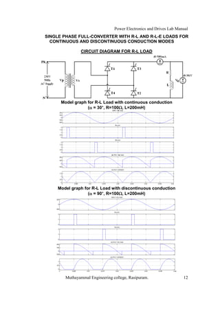
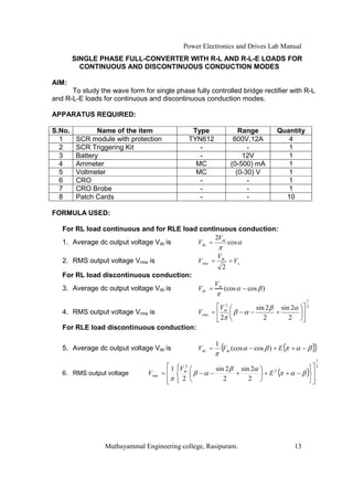
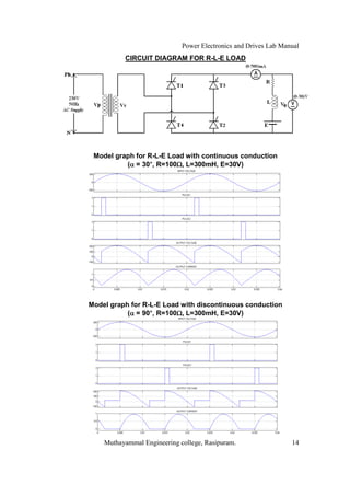
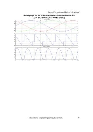
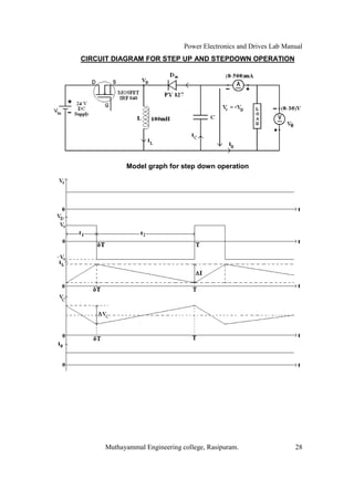
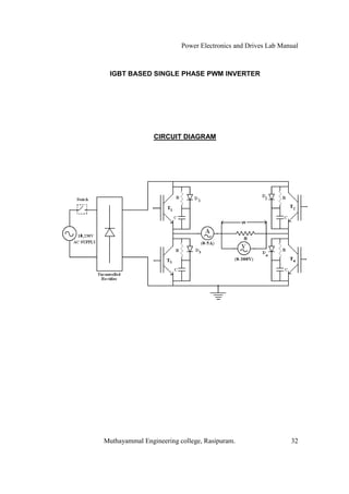
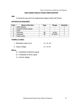
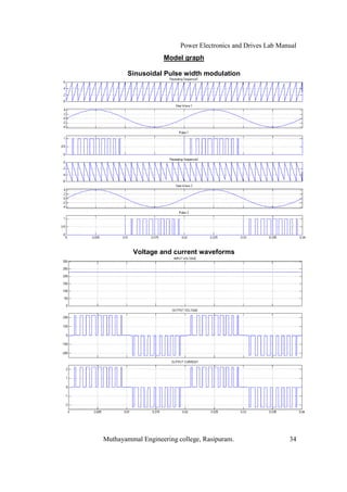
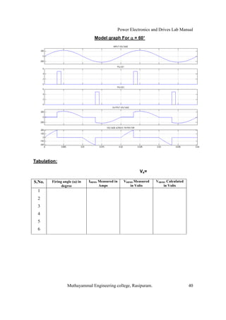

The document is a laboratory manual for power electronics and drives at Muthayammal Engineering College, detailing safety protocols, experimental procedures, and required apparatus for various experiments in the field. It includes instructions for conducting experiments on single-phase and three-phase converters, MOSFETs, and AC voltage controllers, with emphasis on observation, calculations, and record-keeping. Additionally, the manual contains specific circuit diagrams, formulas, and tabulation methods for recording experimental results.