This document provides information about the 8086 microprocessor system architecture including:
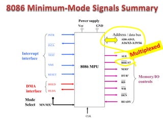
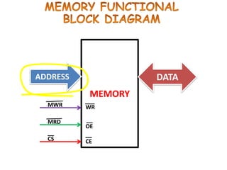
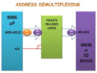
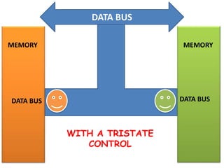
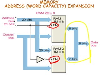
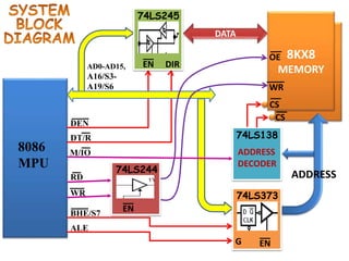
1. Block diagrams showing the connections between the 8086 MPU, memory, I/O devices and support chips.
2. Descriptions of the address/data bus, control signals, and memory/I/O interfacing.
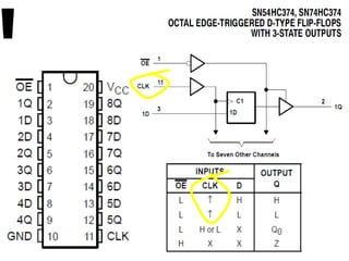
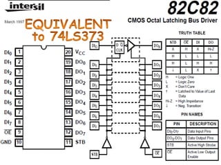
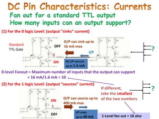
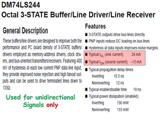
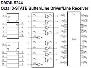
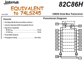
3. Explanations of logic voltage levels, fan-out specifications and tri-state buffers for interfacing TTL devices to the 8086.