1. 32 High Frequency Electronics
Power Amps
Linear Power Amplifiers for
Point-to-Point Radio
Applications
By Sushil Kumar, Kent Story, Ron Kielmeyer, Tariq Lodhi, and Ian Hardcastle—mmW
Solutions Team, RFMD
Microwave links in
the range of 10 – 27 GHz
are commonly used for
point-to-point (P2P) con-
nectivity. With the phe-
nomenal increase of cell
phone users and demand
for high data rates, link
traffic is getting congested. Since available
channel bandwidth is limited and fixed, link
manufacturers are addressing this traffic
congestion by increasing spectral efficiency
and are using a complex modulation scheme
such as 4 – 1024 QAM.
In order to support this high order modu-
lation scheme, there is a need to develop a
new generation of highly linear, high fre-
quency chipsets starting from baseband to
antenna for Tx path and from antenna to
baseband for Rx path.
RFMD has developed a new generation of
chipsets as shown in Figure 1 in the frequen-
cy range of 10 – 27 GHz to address the grow-
ing issue of traffic congestion.
This portfolio includes voltage-
control oscillators (VCOs) featur-
ing state-of-the-art phase noise,
upconverters with best IP3, noise
figure (NF), and LO leakage over
30 dB gain control range, and
downconverters that have
achieved very low NF and high
IIP3 together in their class.
A key to the success of the Tx
chain at a high frequency compo-
nent level is the power amplifier.
As the modulation rate is
increased, the PA’s output power
is backed-off, or in other words, PA output
power is dynamically adjusted during link
operation. The PA should be capable of main-
taining a high level of intermod suppression
(C/I3) at varied output power. In addition, it
needs to have a decent noise figure to mini-
mize error vector magnitude, (EVM), espe-
cially when the PA input signal contains
higher order modulations.
All RFMD PAs referenced in this article
have been designed with these constraints and
limitations in mind and they are packaged in a
6 x 6 QFN package. RFMD’s 10 – 13 GHz lin-
ear PA (RFPA1002) covers 10, 11, and 13 GHz
bands of point-to-point (P2P) link. This PA has
a small signal gain of 26±1 dB, OIP3=37 dBm
at 28 dBm/DCL (Vd=4V, 982mA) and 42 dBm
(at Vd=7V, 1A). The P1dB of this PA is ~+33
dBm. It can also be used as a VGA by adjusting
the gate control voltage. For gain dynamic
range of 15 dB, Pdiss varies from 1.25 W to 6.0
W, worst case IM3 for entire gain dynamic
range is >46 dBc at Pin = -15dBm.
There is a need to
develop a new
generation of highly
linear, high frequency
chipsets to address
traffic congestion.
High Frequency Design
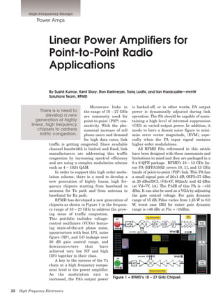
Figure 1 • RFMD’s 10 – 27 GHz Chipset.
2. 34 High Frequency Electronics
High Frequency Design
The RFPA1003 is a 14.4 - 15.4 GHz high linearity PA
and it has been designed for 15 GHz band P2P link. It
has 25 dB gain, IM3=50dBc at POUT
=20dBm/DCL and
35dBc at POUT
=28dBm/DCL. P1dB of this PA is +32.5
dBm and OIP3=42.5 dBm at POUT
=28dBm/DCL.
The RFPA1702 is a 17.7 - 19.7 GHz linear PA. It is
designed for 18 GHz P2P link. It has 25 dB gain,
IM3=52dBc at POUT
=20dBm/DCL and 32.5dBc at
POUT
=27dBm/DCL. P1dB of this PA is +31.0 dBm and
OIP3=41dBm at POUT
=28dBm/DCL. Its power dissipa-
tion is ~7.0 W and NF~7.0 dB. With over 15 dB gain
control, it consumes 2 to 6W dc power and OIP3 varies
from 20 to 40 dBm. The minimum IM3 is >55dBc for
Pin=-15dBm/DCL. All of these PAs have been internally
fabricated using 0.25µm PHEMT technology and pack-
aged in a 6 x 6 QFN package.
Circuit Design
The key to circuit design is the device model. This
model should be able to accurately predict small and
large signal behavior including
P1dB and IM3. The model, which is
developed using DC-IV and
[S]-parameter over various bias
voltages, accurately predicts DC,
[S]-parameters, P1dB and Psat per-
formance. Such models usually
over predict IM3, and its contours
are sometimes severely dislocated
on the Smith Chart compared to
measured contours. RFMD’s PAs
are designed based on a combina-
tion of measured load-pull data and
modified device models to properly
incorporate IM3 behavior and
device scaling based on IM3.
A good technique to PA design is
to partition the spec into number of
stages and then decide the device
size for each stage that should pro-
vide required gain, power, and IM3
per stage and inter-stage drive
ratio. To design a linear power
amplifier one should look for high
gain and best possible IM3 for spec-
ified output power and each device
should be biased for a little higher
Idss compared a saturated power
amplifier design. Normally a satu-
rated power amplifier is biased
close to deep class AB condition.
Agilent’s ADS and Momentum have
been used to design power amplifi-
ers discussed here. Voltage and cur-
rent probes have been used at all
parallel nodes feeding and combin-
ing signal and power to active
device. This helped to determine to
maintain close to identical imped-
ances at all similar nodes and thus
minimize odd-mode problem. Due
to inter-coupling among feed net-
work, impedance mismatch occurs
that cause odd-mode stability
issues. To suppress odd-mode insta-
Power Amps
3. 36 High Frequency Electronics
High Frequency Design
bility, proper value resistors have been added at gates
and drains. ADS S-probe method has been used to check
inter-stage stability. Figure 2 is an example of the
design steps used for design of these PAs. Figure 3a
shows die photographs of 10, 11, 13, 15, and 18 GHz
band PAs. Figure 3b shows PA
outline package drawing. The
main objective of PA design was
to get the best possible IM3 per-
formance at POUT
(total) =28
dBm. Better BW or Psat can be
achieved if IM3 is not the main
design criterion.
Performance of 9.8 - 13.3 GHz
Linear Power Amplifier
(RFPA1002)
Figures 4a - 4f show mea-
suredperformanceofRFPA1002.
This PA covers 10, 11, and 13
GHz bands of P2P application.
All the measurements are taken
at Vd=6.5, Id (total) =1.07A
unless otherwise noted. Figures
4d - 4f show some of the impor-
tant performance plots of this
PA. Figure 4a shows gain ver-
sus frequency behavior over
temperature and Figure 4b
shows OIP3 versus frequency at
drain voltage from 4 to 7V, 0.5
step for single carrier level
(SCL) POUT
= 17dBm (or 20 dBm
total power).
Table 1 shows DC power dis-
sipation corresponding to
Figure 4b. Figure 4c shows
OIP3 improvement with the
increase in DC power dissipa-
tion from 6.8 W to 8.5 W, it
shows > 1.5 dBm improvement
in OIP3 especially at lower fre-
quency and for POUT
= 25dBm/
SCL. The main reason for this
improvement could be due to
slightly mismatched IM3 load-
line between simulation and
measured device output load.
Figures 4d - 4f show measured
performance of the PA as a
VGA. PA gain has been varied
using gate bias. Figure 4d shows
variation of OIP3 versus gain,
total gain was varied about 15
dB and OIP3 was measured at
constant input power=-15dBm/DCL. Figure 4e shows
how gain varies with Vg. A >15dB gain dynamic range
has been achieved by adjusting gate bias. Figure 4f
shows change in DC power dissipation with variation of
Power Amps
4. 38 High Frequency Electronics
High Frequency Design
gain or drain current. Since Vg is varied to get VGA
function, drain current varies with Vg.
Performance of 14.4 - 15.4 GHz Linear Power Amplifier
(RFPA1003)
Figures 5a - 5f show measured performance of
RFPA1003. This is designed for 15 GHz band applica-
tions. All the measurements are taken at Vd=7.5, Id
(total) =1.05A unless otherwise noted. Figure 5a shows
gain versus frequency performance and for entire band
~25dB gain has been achieved. Figure 5b shows IM3
plots with frequency for POUT
= 17/22 and 25dBm SCL.
This PA demonstrates very high IM3 ~50dBc at POUT
=
17dBm/SCL and >32dBc at POUT
= 25dBm/SCL, which is
a key parameter for a linear PA. Figure 5c shows OIP3
versus frequency at POUT
=17/22/25dBm/SCL. Figure 5d
is a plot of P1dB and P3dB versus frequency for PA
when PA bias was tuned for best IM3 or OIP3. If the PA
Power Amps
5. 40 High Frequency Electronics
High Frequency Design
Power Amps
needs to be used as a saturated amplifier, P1dB and
P3dB performance can be improved by tuning bias con-
dition as a saturated amplifier. Figures 5e and 5f show
performance of the PA as a VGA. PA gain has been var-
ied using gate bias.
Performance of 17.7 - 19.7 GHz Linear Power Amplifier
(RFPA1702)
Figures 6a - 6f show measured performance
RFPA1702. This PA covers 18 GHz band of P2P radio
application. All the measurements are taken at Vd=5.5,
Id (total) =1.3A unless otherwise noted. Figures 6a - 6c
show the PAs gain and OIP3 (at POUT
=+15 and +24dBm/
SCL) versus frequency behavior over temperature.
Figure 6c shows P1dB and P3dB behavior of the PA
when biased to achieve best IM3 performance. Figures
6e - 6f show performance of the PA as a VGA. PA gain
has been varied using gate bias.
Conclusion
The performance of RFMD’s linear power
amplifiers is summarized in Table 2. These PAs
demonstrate high gain and high IM3/OIP3 val-
ues at high POUT
(total) = 28 dBm for 10, 11, 13,
and 15 GHz band applications. For 18, 23, and
26 GHz bands, the IM3/OIP3 was measured at
POUT
(total) = 27 and 26 dBm. These PAs show
very good performance as VGAs and, by adjust-
ing gate bias, a gain dynamic range of >15 dB
can be achieved. These PAs maintain decent
IM3/OIP3 performance, a much desired feature
to dynamically adjust power consumption of a
PA. IM5 performance of the PAs is >60 dBc at
POUT
= 22/21 and 20
dBm for the various
bands. P1dB and
Psat was measured
under best IM3 tuned
case, if the amp needs
to be used as a satu-
rated amplifier a dif-
ferent biasing scheme
can be used for better
POUT
performance at
the cost of IM3/OIP3.
All PA designs incor-
porate on-chip pack-
age compensation
networks for good I/O
match and are pack-
aged in a low-cost 6 x
6 ceramic package for
better thermal per-
formance. Due to
superior IM3/OIP3
performance of these PAs, they are well suited for high
data rate and complex modulation systems.
About the Authors:
The authors work at RFMD, where Sushil Kumar is
Director, Engineering; Kent Story is a Staff Design
Engineer; Ron Kielmeyer is a Staff Design Engineer;
Tariq Lodhi is a Senior Design Engineer; and Ian
Hardcastle is a Staff Design Engineer.
References:
1. http://www.rfmd.com/CS/Documents/
RFPA1002DS.pdf
2. http://www.rfmd.com/CS/Documents/
RFPA1003DS.pdf
3. http://www.rfmd.com/CS/Documents/
RFPA1702DS.pdf
Table 2 • Summary of RFMD’s Linear Power Amplifiers.

![34 High Frequency Electronics
High Frequency Design
The RFPA1003 is a 14.4 - 15.4 GHz high linearity PA
and it has been designed for 15 GHz band P2P link. It
has 25 dB gain, IM3=50dBc at POUT
=20dBm/DCL and
35dBc at POUT
=28dBm/DCL. P1dB of this PA is +32.5
dBm and OIP3=42.5 dBm at POUT
=28dBm/DCL.
The RFPA1702 is a 17.7 - 19.7 GHz linear PA. It is
designed for 18 GHz P2P link. It has 25 dB gain,
IM3=52dBc at POUT
=20dBm/DCL and 32.5dBc at
POUT
=27dBm/DCL. P1dB of this PA is +31.0 dBm and
OIP3=41dBm at POUT
=28dBm/DCL. Its power dissipa-
tion is ~7.0 W and NF~7.0 dB. With over 15 dB gain
control, it consumes 2 to 6W dc power and OIP3 varies
from 20 to 40 dBm. The minimum IM3 is >55dBc for
Pin=-15dBm/DCL. All of these PAs have been internally
fabricated using 0.25µm PHEMT technology and pack-
aged in a 6 x 6 QFN package.
Circuit Design
The key to circuit design is the device model. This
model should be able to accurately predict small and
large signal behavior including
P1dB and IM3. The model, which is
developed using DC-IV and
[S]-parameter over various bias
voltages, accurately predicts DC,
[S]-parameters, P1dB and Psat per-
formance. Such models usually
over predict IM3, and its contours
are sometimes severely dislocated
on the Smith Chart compared to
measured contours. RFMD’s PAs
are designed based on a combina-
tion of measured load-pull data and
modified device models to properly
incorporate IM3 behavior and
device scaling based on IM3.
A good technique to PA design is
to partition the spec into number of
stages and then decide the device
size for each stage that should pro-
vide required gain, power, and IM3
per stage and inter-stage drive
ratio. To design a linear power
amplifier one should look for high
gain and best possible IM3 for spec-
ified output power and each device
should be biased for a little higher
Idss compared a saturated power
amplifier design. Normally a satu-
rated power amplifier is biased
close to deep class AB condition.
Agilent’s ADS and Momentum have
been used to design power amplifi-
ers discussed here. Voltage and cur-
rent probes have been used at all
parallel nodes feeding and combin-
ing signal and power to active
device. This helped to determine to
maintain close to identical imped-
ances at all similar nodes and thus
minimize odd-mode problem. Due
to inter-coupling among feed net-
work, impedance mismatch occurs
that cause odd-mode stability
issues. To suppress odd-mode insta-
Power Amps](data:image/gif;base64,R0lGODlhAQABAIAAAAAAAP///yH5BAEAAAAALAAAAAABAAEAAAIBRAA7)