Download to read offline


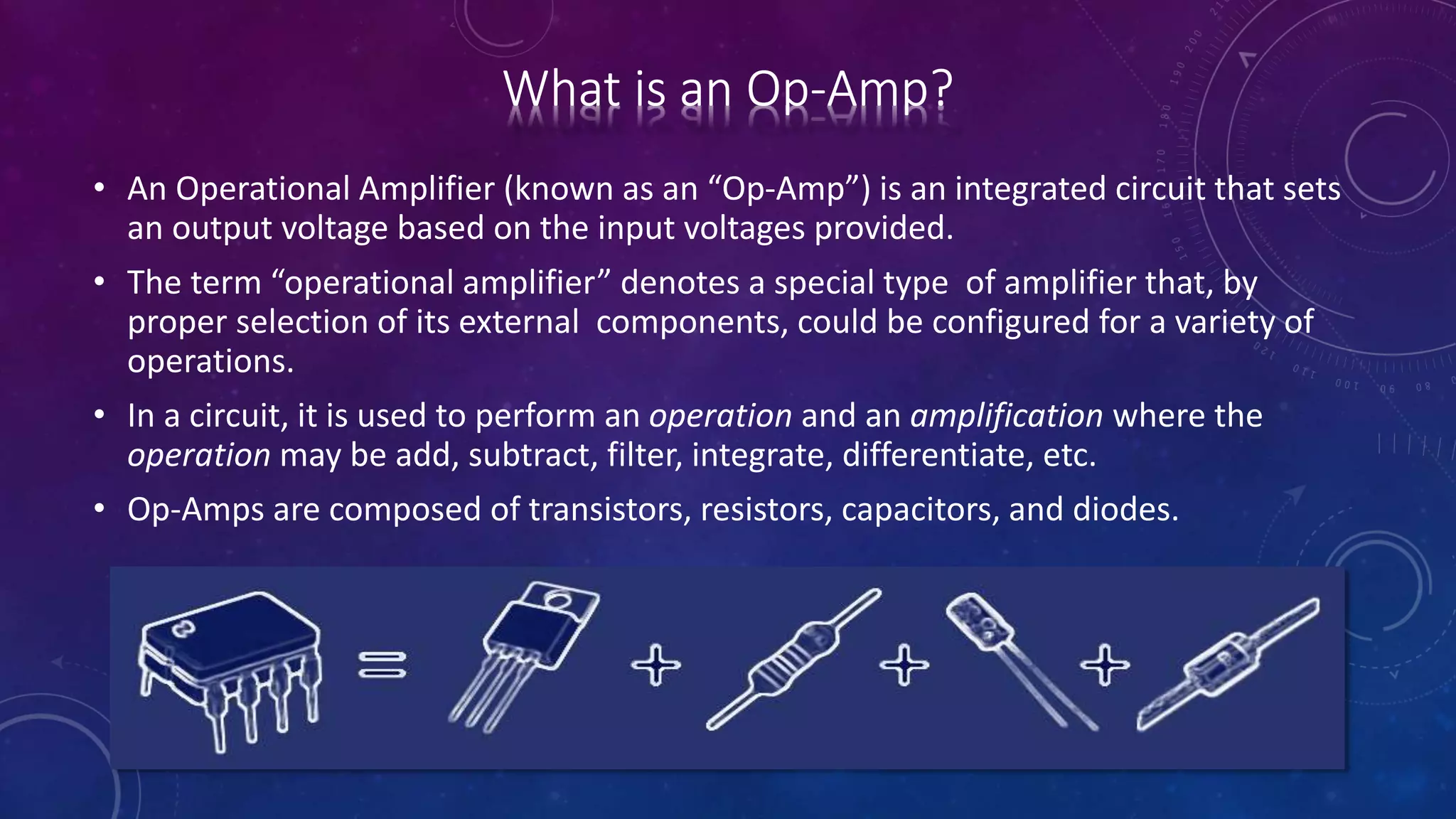


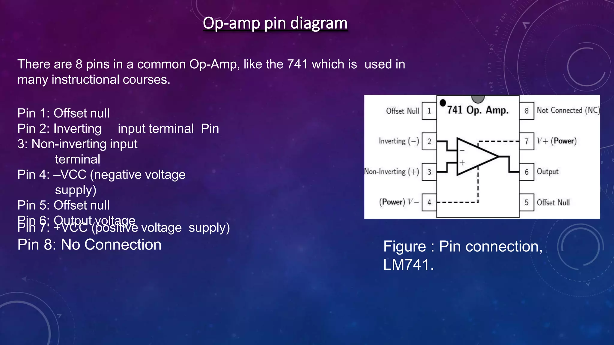


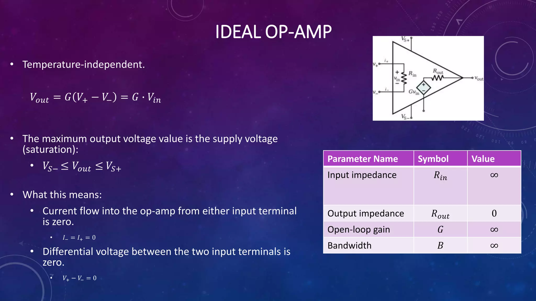
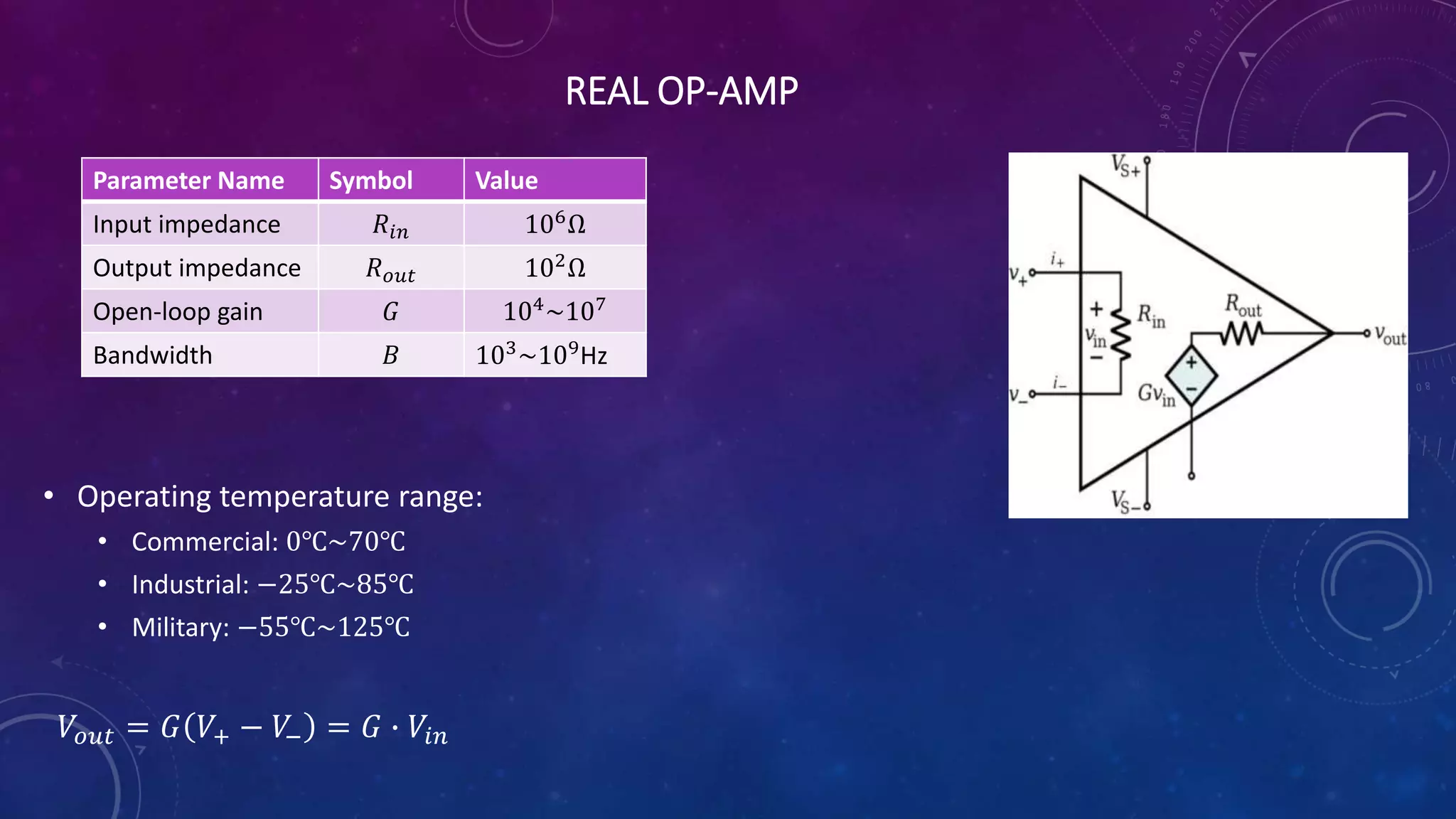


The document provides a comprehensive overview of operational amplifiers (op-amps), detailing their history, characteristics, applications, advantages, and disadvantages. It traces the development of op-amps from their inception in 1941 to their current advanced forms and discusses ideal versus real op-amp parameters, highlighting their universal application in analog tasks. Additionally, it outlines specific uses such as A/D converters and zero crossing detectors, along with the challenges faced by conventional op-amps.