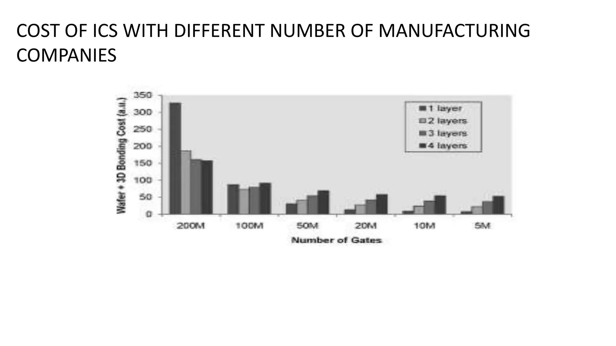
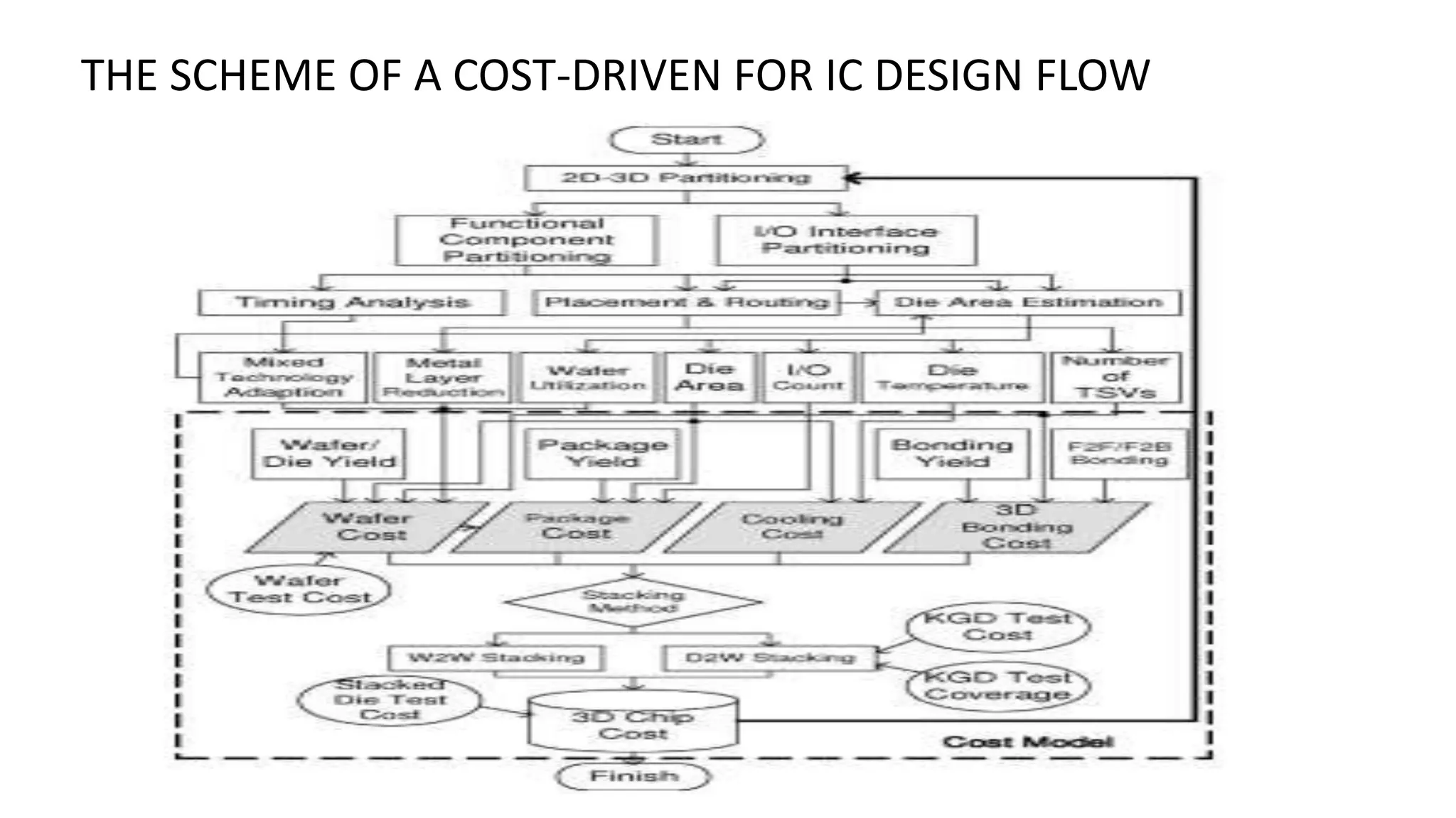
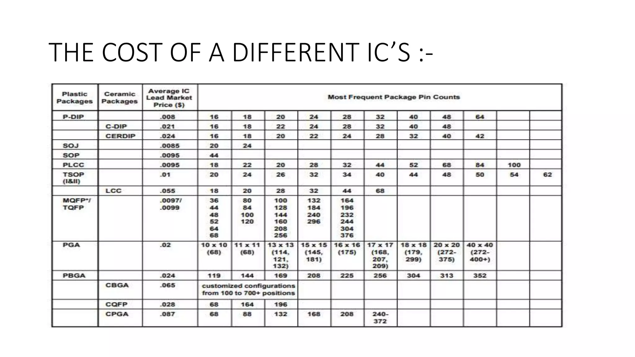
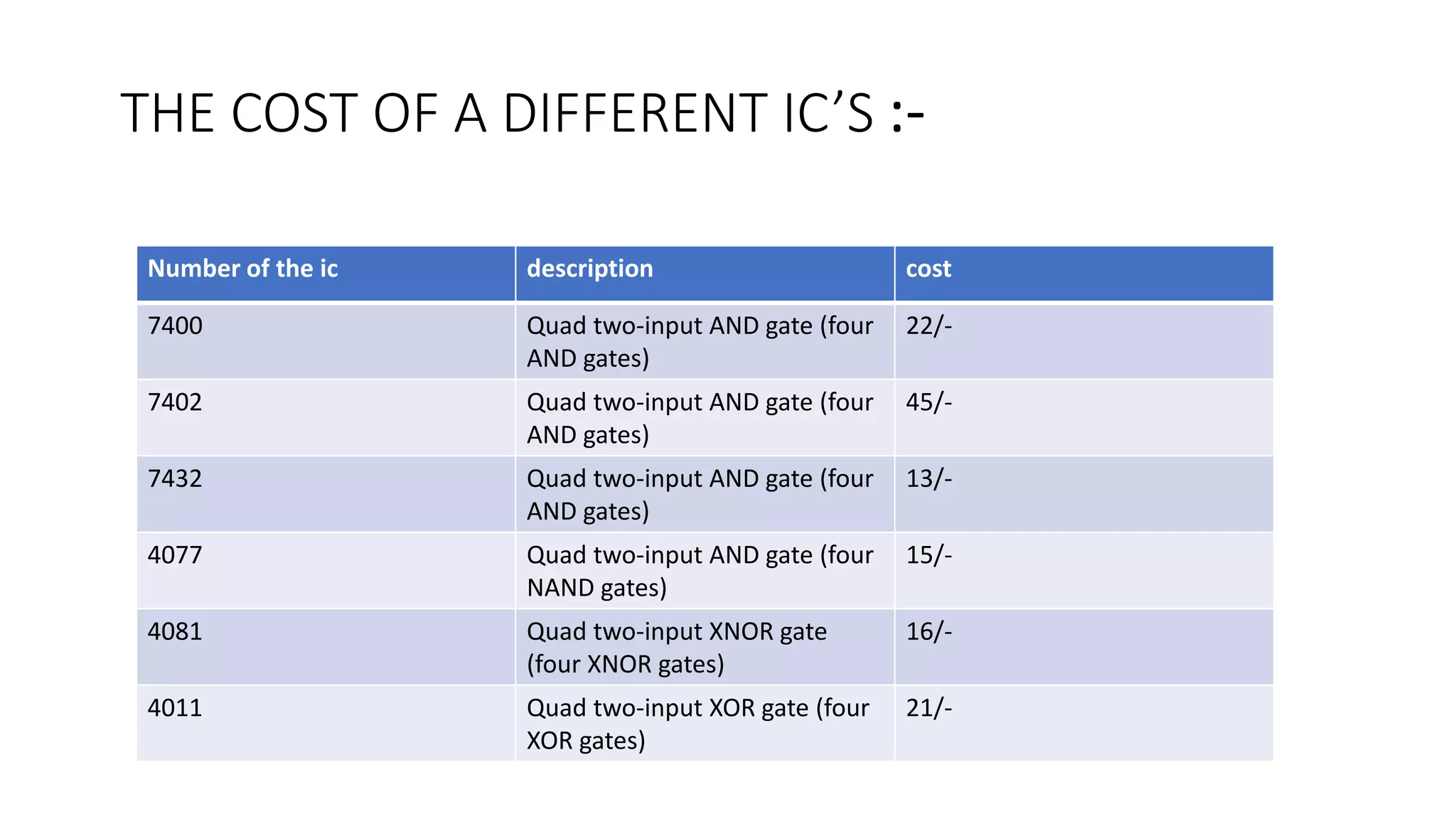
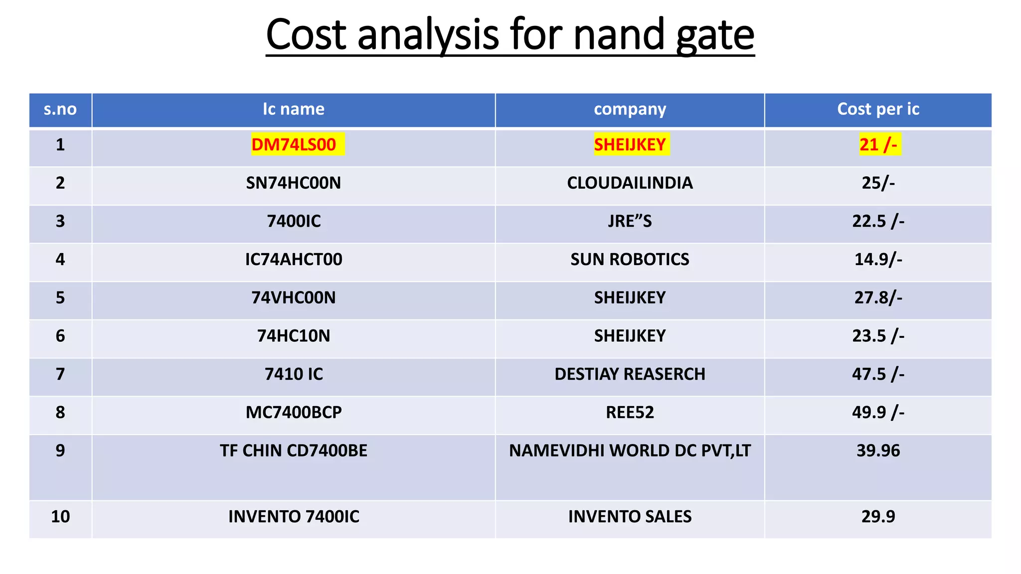
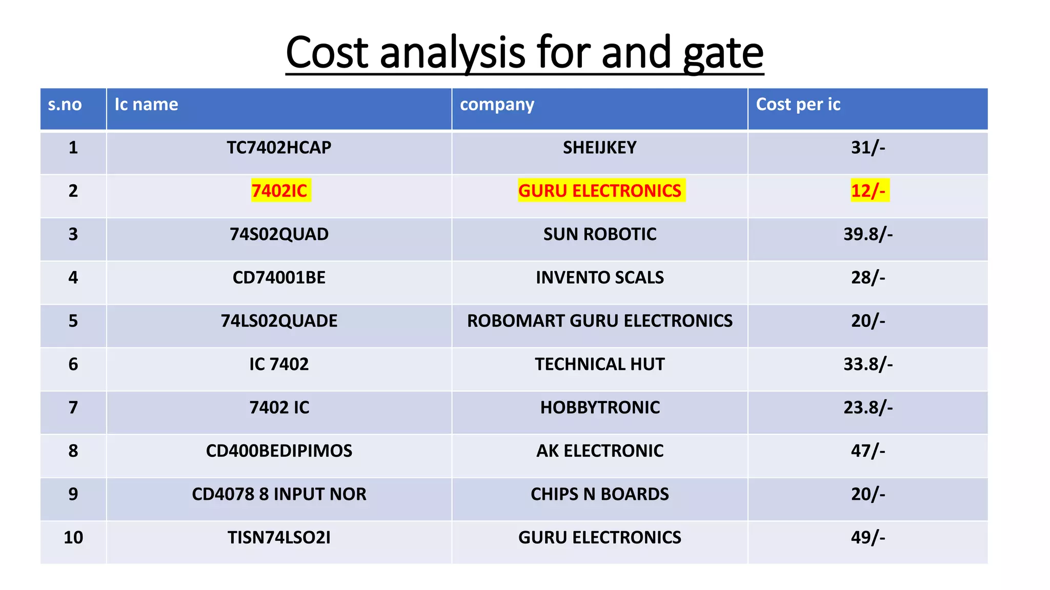
A sequential circuit is formed from a combinational circuit and storage elements. The circuit's state is defined by the information stored at any given time. The next state depends on the current inputs and state. A synchronous sequential circuit's behavior can be described at discrete time instances. It was designed as a Moore state machine to detect the "1101" sequence, with the output associated with the state. VHDL code implements it with a process changing the state variable based on the present state and input to determine the next state and output.
Shift registers are digital circuits composed of flip-flops that can shift data from one stage to the next. They can be configured for serial-in serial-out, serial-in parallel-out, parallel-in serial-out, or parallel-in parallel-out data movement. Common applications include converting between serial and parallel data, temporary data storage, and implementing counters. MSI shift registers like the 74LS164 and 74LS166 provide 8-bit shift register functionality.
This document discusses latches and flip flops, which are types of sequential logic circuits. It describes the basic components and functioning of latches like SR latches, D latches, and gated latches. For flip flops, it covers SR flip flops, D flip flops, JK flip flops, and master-slave flip flops. The key differences between latches and flip flops are that latches do not have a clock input while flip flops are edge-triggered by a clock signal. Latches and flip flops are used as basic storage elements in more complex sequential circuits and in computer components like registers and RAM.
This document provides information about different types of counters, including asynchronous counters, synchronous counters, MSI counters, and specific counter integrated circuits. It defines counters and describes their basic characteristics. It discusses asynchronous ripple counters and their timing. It provides examples of decade and binary counters. It describes synchronous counters and MSI counters like the 74LS163 4-bit synchronous counter. Finally, it provides truth tables, logic diagrams, and application information for common counter ICs like the 7490, 7492, 7493, and 74LS163.
Sequential circuits consist of combinational logic and memory elements like latches and flip-flops. There are different types of latches and flip-flops that differ in their trigger mechanisms and outputs, including SR latches, D latches, and edge-triggered flip-flops like SR, D, and JK flip-flops. Asynchronous inputs can directly set or reset flip-flop outputs independent of the clock signal.
This document provides examples of VHDL code for modeling basic logic gates and multiplexers. It begins with syntax for VHDL programs and then provides behavioral VHDL code for modeling common logic gates like AND, OR, NOR, NAND, XOR and XNOR gates. It also provides code for half adder, full adder, half subtractor and full subtractor. The document further contains VHDL code examples to model a 4-to-1 multiplexer and 1-to-4 demultiplexer using different types of statements like if-else, case, when-else and with-select.
Project report on the Digital clock using RTC and microcontroller 8051Maulik Sanchela
1. The document describes a project report for a digital clock circuit with time and alarm functions. The circuit uses an RTC chip to accurately display the time and date. It can set the time and alarm and displays it on an LCD.
2. The circuit diagram shows how the RTC connects to the microcontroller and how it continuously reads the RTC data and processes it to display the correct time on the LCD. It uses buttons to set the time and alarm.
3. The project aims to design an accurate digital clock with functions to set the time and alarm using common electronic components like a microcontroller, RTC, LCD, and buttons.
Presentation knock door bell project by namitNamit Sood
knock to ring bell project ppt by namit easily explained
contact me for all kinds of electronics project and web development,other software related problem
Registers are used to store binary numbers and consist of groups of flip flops, with one flip flop per bit. There are four basic types of registers: serial in serial out, serial in parallel out, parallel in serial out, and parallel in parallel out. Shift registers are groups of flip flops connected to allow data to be entered and shifted. Data can be shifted either serially or in parallel. Common integrated circuits used include the 74164 for serial in parallel out and 74191 for serial in serial out.
The document discusses the 8051 microcontroller. It describes the basic components of the 8051 including 4K bytes of internal ROM, 128 bytes of internal RAM, four 8-bit I/O ports, two 16-bit timers/counters, and one serial interface. It also provides details on the block diagram, important pins like ports and serial interface pins, and how to connect an external clock source to the 8051.
1. The 8254 contains three independent 16-bit counters/timers that can be programmed to operate in different modes.
2. Each counter can be programmed to count from 1 to 65535 and has a programmable control word to select the operating mode.
3. The 8254 supports various timer modes like one-shot, continuous square wave, event counter, and software/hardware triggered one-shot for applications like timing, delay generation, and pulse width modulation.
The document provides an overview of the Analog and Digital Electronics course taught at Matoshri College of Engineering & Research Centre. It includes information about the course's teaching scheme, examination scheme, objectives, and outcomes. The objectives are to design logical, sequential and combinational digital circuits using K-maps and to develop concepts related to operational amplifiers and rectifiers. The document also provides details of the topics to be covered in the first unit including Boolean algebra, K-maps, and the design of combinational circuits. It introduces concepts such as logic gates, number systems, and digital signals.
This document discusses different logic families including Resistor Transistor Logic (RTL), Diode Transistor Logic (DTL), Transistor-Transistor Logic (TTL), and Emitter Coupled Logic (ECL). It provides circuit diagrams and explanations of the working principles for each logic family. Key characteristics like fan-in, fan-out, propagation delay, noise immunity, and power dissipation are compared for each logic family.
Programmable logic devices (PLDs) allow users to implement digital logic designs on a single chip. PLDs have advantages over traditional integrated circuits like lower costs for lower production volumes and shorter design times. Common types of PLDs include simple programmable logic devices like PALs, GALs, and CPLDs. PLDs are configured using memory like SRAM, EPROM, EEPROM, or flash to store the programmed logic pattern. Reprogrammability allows PLDs to be reused for different logic functions.
This document describes an R-2R ladder digital-to-analog converter (DAC). It explains that an R-2R ladder DAC uses only two resistor values, R and 2R, to convert a binary input signal into an analog output voltage. The circuit diagram and working of the R-2R ladder is provided. A 4-bit R-2R ladder DAC is simulated showing the output combinations. Advantages like only needing two resistor values and ability to expand bits are discussed. Applications like audio amplifiers and motor control are also listed.
Group members for the project are Falah Hassan, Maidah Malik, and Maria Khan. The document discusses half adders and full adders. A half adder adds two binary digits and produces a sum and carry output. It is built from two logic gates. A full adder accepts two input bits and a carry input, and produces a sum and carry output. It is implemented using two half adders joined by an OR gate. The main difference between a half adder and full adder is that a full adder has three inputs and two outputs, allowing multiple adders to be chained to add more bits.
The document contains a list of 23 microprocessor lab programs and 6 interfacing programs for an electronics and communication course. The programs cover topics like data transfer, arithmetic operations, sorting, prime number generation, string operations, matrix multiplication and more. The document provides contents, program descriptions and assembly language code for some of the programs.
The document discusses interrupts for the PIC18 microcontroller. It explains that interrupts allow the microcontroller to instantly respond to events like pin changes or timer overflows. When an interrupt occurs, the microcontroller stops executing the main program and jumps to the interrupt service routine (ISR) to handle the interrupt. It provides details on enabling and disabling interrupts, the interrupt vector table, and examples of using interrupts for external pins, timers, and serial communication.
The 8051 microcontroller has an 8-bit CPU, 4K ROM, 128 bytes RAM, two 16-bit timers, 32 I/O lines, and serial port. It uses an accumulator, B register, program status word and stack pointer along with arithmetic logic unit and instruction decoder to perform operations. The memory includes internal ROM, RAM, and external memory accessed via a 16-bit data pointer and program counter.
This document discusses digital to analog converters (DACs). It explains that a DAC converts digital numbers into analog voltages or currents. The key components of a DAC are its digital input, analog output, and conversion process. Common DAC types include binary weighted resistor DACs and R-2R ladder DACs, which use resistors and switches to implement the conversion. Important DAC specifications are also outlined such as reference voltage, resolution, speed, settling time, and linearity. Common applications of DACs include function generators, digital oscilloscopes, and converting digital video signals to analog formats for display.
This document discusses different types of flip-flops including edge-triggered flip-flops like the S-R, D, and J-K flip-flops. It describes their characteristics such as how their output changes depending on the input and clock signal. The S-R flip-flop can be set or reset. The D flip-flop copies its input to the output on the clock edge. The J-K flip-flop can toggle its output. The T flip-flop is a single-input version of the J-K flip-flop that toggles its output. Flip-flops have applications in data transfer and frequency division.
A microcontroller is a single-chip microprocessor system consisting of a CPU, memory, and input/output ports. It can be considered a complete computer on a single chip. The 8051 was an early microcontroller developed by Intel for use in embedded systems. It had 4KB of program memory, 128 bytes of data memory, timers, counters, and I/O ports. The 8051 has separate memory spaces for program and data memory and its CPU, registers, timers and I/O ports allow it to monitor and control external devices.
Shift registers are constructed using flip-flops connected in a way to store and transfer digital data. Data is stored at the Q output of D flip-flops during a clock pulse. Shift registers allow data to be transferred between flip-flops upon a clock edge. There are four types of data movement: serial in serial out, serial in parallel out, parallel in serial out, and parallel in parallel out. Shift registers can be loaded serially or in parallel and are used in applications like pseudo random pattern generators, ring counters, and Johnson counters.
This document provides an introduction and overview of microcontrollers. It begins by defining a microcontroller as a single-chip computer containing a CPU, RAM, ROM, I/O ports, and other peripherals. It then discusses the 8051 microcontroller in more detail, outlining its addressing modes, block diagram, operation, features, applications, and advantages over microprocessors. Finally, it provides a pin description and diagram of the 8051 microcontroller.
Synchronous loadable up and down counter is a very important block in any complex digital system design. It is not just used for counting, it is also used for phase signal generation, clock division and for initiation of a process.
Microcontroller 8051 and its interfacingAnkur Mahajan
The document discusses microcontrollers and interfacing. It begins with definitions of microprocessors and microcontrollers, comparing their differences. It then focuses on the 8051 microcontroller, describing its features, block diagram, manufacturers, and addressing modes. The document outlines how to write programs for the 8051 and discusses real-world interfacing examples like LCDs, ADCs, relays, motors. It concludes with applications of the 8051 and contact information.
HDT Italia produces EDA tools for signal integrity, hardware modeling, and EMC/EMI analysis and validation. Their main product is PRESTO, which uses the SPRINT simulation engine to enable fast, exhaustive simulation of entire printed circuit boards. PRESTO can analyze signal integrity issues, EMC/EMI compliance, and validate design functionality. It produces detailed reports and can interface with measurement equipment for validation. HDT also provides consulting services and the EmiR tool for predicting radiated emissions from PCB designs.
EMCLO PROJECT: EMC DESIGN METHODOLOGY FOR LAYOUT OPTIMIZATIONPiero Belforte
This project aimed to develop and validate a prototype EMC simulation tool called PRESTO_CNT. The tool allows predictive analysis of EMC problems on PCBs and optimization of critical tracks through simulation. It was tested on a lights control PCB from Magneti Marelli, comparing simulations of injected noise to measurements. The results demonstrated the viability of the tool and showed good agreement between simulation and measurement. The tool and EMC modeling methodology developed in this project could help improve PCB design processes and reduce product development time at Magneti Marelli.
Optimization of Threshold Voltage for 65nm PMOS Transistor using Silvaco TCAD...IOSR Journals
This document summarizes research optimizing the threshold voltage (VTH) for a 65nm PMOS transistor using Silvaco TCAD simulation tools. The researchers varied three fabrication factors - gate oxide thickness, channel doping concentration, and channel implantation concentration - in the simulation. The simulation results showed a VTH value of -2.55427V for a 65nm PMOS transistor with a gate oxide thickness of 0.0025um, boron channel doping of 2x10¹⁵, and phosphorus implantation of 3.5x10¹³ atom/cm-1. Thicker gate oxides, higher channel doping, and increased implantation concentrations each caused higher VTH values in the simulation, consistent with theoretical expectations.
MERITA PROJECT:METHODOLOGY TO EVALUATE RADIATED EMISSION FROM HIGH DENSITY MU...Piero Belforte
1) The document describes a methodology for evaluating radiated emissions from multilayer printed circuit boards using a software tool called PRESTO_POWER.
2) PRESTO_POWER simulates high-speed PCBs taking into account electromagnetic compatibility phenomena like bouncing on power planes and evaluating power current loops.
3) It allows modeling of power and signal planes through a gridding algorithm to identify current loops and evaluate their impact on radiated emissions.
wireless charging of an electrical vechicle 4hari prasad
This presentation discusses wireless power transfer for electric vehicle charging systems. It introduces various wireless power transfer methods like electromagnetic induction and microwave radiation. Electromagnetic induction involves using a transmitter coil to generate a magnetic field that induces a voltage in a receiver coil. The presentation compares different techniques and outlines a project to design a wireless charging system using an inverter, transmitter and receiver coils, and rectifier. It also discusses components like ICs, Arduino, and coil design considerations. The expected outcomes are wireless battery charging for applications like pacemakers to eliminate regular operations and enabling electric vehicles to charge safely at regular distances.
IRJET- A Novel Design of Flip Flop and its Application in Up CounterIRJET Journal
1) The document proposes a novel design of flip flops and a 4-bit up counter using Quantum-Dot Cellular Automata (QCA) technology. QCA is an emerging nanotechnology that could overcome scaling limitations of CMOS.
2) In QCA, logic states are represented by the position of electrons in quantum dots rather than voltage as in CMOS. Basic logic gates like inverters and majority gates are constructed using QCA cells.
3) The document designs various flip flops like SR, JK, D, and T flip flops in QCA and uses them to build a 4-bit up counter. Power consumption is shown to be lower for the QCA designs compared to
Programmable ac power control system newAman Bharti
This document describes a student project to create a programmable AC power control system. It includes a list of components needed for the circuit as well as the modes of operation for the project, which involve controlling the speed and power output to a bulb. It also describes interfacing the system with sensors to detect over voltage and temperature problems and trigger alerts or automatic responses. The project aims to demonstrate concepts of power control, energy saving, and industrial automation using a microcontroller.
IBIS MODELING FOR WIDEBAND EMC APPLICATIONSPiero Belforte
1) The document discusses electrical modeling techniques for predicting signal integrity (SI) and electromagnetic emissions from printed circuit boards. Accurate models of device I/O characteristics are needed that consider minimum and maximum parameter values.
2) Measuring the dynamic transfer function (DTF) of device I/O using a time domain reflectometer is important for modeling the high frequency behavior that influences electromagnetic emissions, even for low speed circuits.
3) With an accurate DTF measurement and statistical ranges for key parameters, the models can correctly simulate signals and match measured emission levels, validating the modeling approach for design stage EMC predictions.
This document contains the lab manual for a digital electronics course. It outlines 10 experiments involving logic gates and circuits, including studying logic gates, universal gates, half and full adders/subtractors using logic gates, and designing 4-bit adders and subtractors using the IC 7483. The experiments are meant to help students learn about basic digital logic components and how to design circuits using gates to perform arithmetic operations like addition and subtraction.
In digital logic and computing, a counter is a device which stores the number of times a particular event or process has occurred, often in relationship to a clock signal. CMOS devices are designed for high noise immunity and low static power consumption. CMOS accomplishes current reduction by complementing every nMOSFET with a pMOSFET and connecting both gates and both drains together. A high voltage on the gates will cause the nMOSFET to conduct and the pMOSFET to not conduct, while a low voltage on the gate causes the reverse. This arrangement greatly reduces power consumption and heat generation .Finally we proposed counter using SRAM model, provides the best resolution, high output current and good output-input current linearity.
DEVELOP A SOUND SENSOR USING LM 324 AND MICROPHONE.pptxAshish Sadavarti
The document describes a microproject seminar on developing a sound sensor using an LM324 integrated circuit and microphone. It was guided by Miss Rita Pawade and involved team members Pritosh Khanwe, Rahul Warade, Shital Ganeshkar, Rohan Meshram, and Ruchika Bangale from the Electronics and Telecommunication Engineering department of NIT Polytechnic Nagpur. The objectives were to understand how a sound detector works and develop technical skills. The circuit diagram and working of the sound sensor are provided, along with applications such as security systems and skills developed like problem solving.
This document outlines the course Digital Electronics & Logic Design taught by Dr. Vivek Garg at S. V. National Institute of Technology. The course covers topics such as shift registers, counters, sequential circuit analysis, state reduction, and sequential circuit design. Shift registers are arrays of flip flops that can store bits in serial or parallel configurations. Counters are used to count clock pulses and for applications like frequency division. Sequential circuit analysis involves obtaining the state table or diagram. State reduction aims to minimize the number of states and flip flops. The design process for sequential circuits specifies the states and derives the logic diagram.
Implementing Electrical and Simulation Rule Checks to ensure Signal QualityEMA Design Automation
Join Matthew Harms as he discusses a unique multi-tiered strategy to board analysis & verification designed to enable designers of all skill levels to analyze their PCB designs early in the development cycle when the cost of change is the lowest. Matthew will show how Cadence has created a multi-tier analysis environment that lets designers start with a set of pre-defined Electrical Rule Checks (ERC) that can be run on the board to quickly identify areas of interest or concern all without the need for any complex models or configurations. Based on these initial 1st order results Matthew will show how design teams can then effectively target critical nets with 2nd order (Simulation Rule Checks) and 3rd order (Power Aware Signal Integrity) analysis as needed to simulate with greater detail and achieve complete electrical design signoff.
This document discusses the design and implementation of a sequential state machine using integrated circuit techniques. It begins with an introduction that provides an overview of digital systems and sequential system design. It then discusses various logic design techniques for implementing sequential circuits, including programmable logic devices (PLDs), gate arrays, and standard cell-based systems. The rest of the document will discuss the design process for a sequential state machine and its implementation using these techniques.
IRJET- Review on Performance of OTA StructureIRJET Journal
This document reviews several studies on operational transconductance amplifier (OTA) based analog filter circuits. It discusses OTA based single input single output, multi input single output, and single input multi output filter circuit topologies. It also summarizes key contributions from several papers that proposed new OTA based filter circuits, including biquad filters, oscillators, and rectifiers. The proposed circuits aim to achieve features like independently tunable frequency and quality factor responses, low component counts, and suitability for integrated circuit implementation. PSPICE simulation results confirming the theoretical analyses are also mentioned.
The document describes a PC-based oscilloscope that can display input waveforms on a computer screen. It includes a block diagram of the circuit which conditions input signals below 1 kHz and converts them to digital format for interfacing with a PC. Software written in Turbo C acquires and displays the data. The PC-based oscilloscope costs less than traditional models, can store multiple waveforms, and allows viewing on multiple PCs over a network. However, it has limitations such as low input frequency and voltage range and lacks multi-channel capability.
This document discusses limitations of traditional serial scan design for testing integrated circuits and proposes an alternative called Random Access Scan (RAS). RAS addresses three key limitations of serial scan: 1) test data volume, 2) test application time, and 3) test power. In RAS, flip-flops act as addressable memory elements during test mode, reducing time to set and observe flip-flop states compared to serial scan. While RAS requires more gates and test pins than serial scan, it significantly reduces switching activity and power consumption during testing.
Implementation of Reversable Logic Based Design using Submicron TechnologySai Viswanath
Reversible logic has emerged as a computing paradigm having application in low power CMOS, quantum and optical computing. Design of reversible logic gate is reversible operation, when we say reversible it performing computation in such a way that any previous state can be reconstructed at given a description of the current state. The classical set of gates such as AND, OR, and XOR are not reversible.
This presentation is a design of reversible logic gate used for reversible operation. When we say reversible computing, we mean performing computation in such a way that any previous state of the computation can always be reconstructed given a description of the current state. The classical set of gates such as AND, OR, and EXOR are not reversible. This paper also includes simulation results of forward & backward computation of reversible FREDKIN gate and TSG gate.
The document describes a student project on an automatic railway gate control system. It includes a declaration signed by four students stating that the work is original. It also includes an acknowledgements section thanking their supervisor and institution for support and resources. The abstract provides a brief overview of the system, which uses sensors to automatically open and close railway gates based on a train's proximity.
Automatic Power Factor Corrector Using Arduino reportSelf-employed
This document describes an automatic power factor corrector system using an Arduino microcontroller. The system measures the power factor of a load by determining the phase difference between the line voltage and current signals. It then calculates the required compensation and switches capacitors from a capacitor bank to normalize the power factor close to unity. This improves the efficiency of the power system by reducing losses. The automatic correction allows for varying loads by adjusting the capacitors proportionately.
Similar to digital electronics Design of 101 sequence detector without overlapping for mealy FSM and Perform cost analysis (20)
THIS DOCUMENT IS MAINLY PREPARED ON THE TIME RESPONSE OF A SECOND ORDER SYSTEM AND IN THIS DOCUMENT WE ALSO DONE THE SIMULATION BY USING MATLAB AND HERE WE ALSO DONE THE THEORETICAL MATHEMATICAL CALCULATIONS TO SHOW HOW THE SYSTEM IS BEHAVING IN DIFFERENT CONDITIONS AND HERE WE ALSO DONE THE MATLAB CODING AND THE RESULTS ARE ALSO PLOTTED IN THE DOCUMENT
THIS PPT IS DONE ON THE MICROGRID. IN THIS PPT WE DISCUSSED THE USES OF MICROGRIDS AND THEIR REAL-LIFE APPLICATIONS AND HOW THEY ARE INTERCONNECTED TO EACH OTHER AND THE MAJOR DIFFERENCE BETWEEN THE CONVENTIONAL GRIDS AND THE MICROGRIDS AND THEIR USES, ADVANTAGES ARE ALSO DISCUSSED IN THIS PRESENTATION AND USES IN FUTURE ALSO AND THIS PPT IS SO USEFUL TO MANY STUDENTS
THIS IS A PROJECT DONE BY USING SMALL ELECTRONICS COMPONENTS AND BY DOING THIS WE CAN SEE THE FADING OF LED BY UP AND DOWN AND FOR THIS WE MADE REPORT IN A SPECIFIED WAY AND IN THIS IS WE SHOWN EVERY STEP BRIEFLY HOW TO DO THE PROJECT AND THE RESULTS ARE ALSO COMING AND THIS PROJECT IS USEFUL FOR MANY TO DO PROJECTS
THIS DOCUMENT MAINLY CONTAINS THE HOW TO MODLE DC SERVO MOTOR BY USING THE MATLAB SIMULINK AND HOW IT WILL BEHAVE IS SHOWN IN THE MATHEMATICAL EQUATIONS AND THE PLOTTINGS ARE ALSO KEPT IN THIS DOCUMENT SO BY THIS IT IS USEFUL TO STUDY THE CHARACTRISTICS OF A DC SERVO MOTOR
THIS PPT IS MAINLY BASED ON HOW THE ELCTRONIC FUEL INJECTION SYSTEMS IN DIFFERENT VEHICLES AND IN THIS WE HAVE DISCUSSED DIFFERENT TECHNIQUES IN DIFFERENT VEHIOCLEWS AND THEIR MODELS ALSO AND THEIR SYSTEMS ALSO IN THE VEHICLES AND THEIR COMPONENTS AND THEIR USES ARE ALSO MENTIONED IN THIS PPT SO IT IS USEFUL FOR BOTH MECHANICAL AND ELECTRONICS STUDENTS
THIS PPT IS MAINLY CONTAINS THE GREEN ENERGY TECHNIQUES AND THE USES OF USING RENEWABLE ENERGY RESOURCES AND IN THIS WE ALSO DISCUSSED THE VARIOUS TYPES OF ENERGIES AVAILABLE AND THEIR REQUIREMENTS IN THE FUTURE AND IT IS USEFUL
THIS DOCUMENT CONTAINS THE DIGITAL ELECTRONICS DESIGN OF 3 BIT MAJORITY CIRCUIT. IN THIS DOCUMENT THERE IS A BRIEF EXPLANATION ABOUT THE CIRCUIT HOW TO DESIGN AND IMPLEMENTATION OF CIRCUIT AND THE THEORETICAL CALCULATIONS,TRUTH TABLES ARE ALSO DONE IN THIS DOCUMENT AND THIS IS USEFUL FOR THE ELECTRONICS STUDENTS
THIS PPT IS MAINLY BASED ON ELECTRICAL CIRCUIT ANALYSIS PROBLEM AND THIS PPT ALSO SOLVED THEORETICALLY AND SOLVED BY USING THE MATLAB SOFTWARE AND THIS ALSO CONTAINS THE CODE AND RESULTS ARE ALSO THERE.SO THIS IS USEFUL
power systems ppt on Arc welding and Electric welding equipment and compariso...sanjay kumar pediredla
this ppt is mainly based on the power systems related topic and in this ppt mainly consists of ac and dc weldings and which welding is used mainly and the importance of arc welding and electric welding and the techniques are also discussed in this and it is so helpful .and the safety requirements and the equipment used is also discussed in this topic
CONTROL SYSTEM PPT ON DETERMINATION OF SABILITY OF SYSTEM USING NYQUIST PLOT ...sanjay kumar pediredla
This document discusses using the Nyquist plot to determine the stability of a control system. It provides an example of a stable system where the Nyquist plot does not encircle the -1 point, indicating no zeros in the right half plane and stability. An unstable example is also given where the plot encircles the -1 point twice, indicating two zeros in the right half plane and instability. The behavior of the Nyquist plot at high frequencies is explained. MATLAB is referenced for generating Nyquist plots from transfer functions.
CONTROL SYSTEMS PPT ON A UNIT STEP RESPONSE OF A SERIES RLC CIRCUIT sanjay kumar pediredla
THIS PPT IS SO USEFUL TO KNOW ABOUT THE SERIES RLC CIRCUIT AND IN THIS WE CAN ALSO HOW THE RESPONSE WILL BE THERE FOR A UNIT STEP RESPONSE AND I ALSO KEPT A MATLAB CODING AND GRAPHS FOR THE SERIES RLC CIRCUIT
DESIGN OF CIRCUIT DEBITS THE GIVEN VALUE TO THE DEFAULT VALUE WITH COST ANAL...sanjay kumar pediredla
THIS REPORT IS BASED ON THE DESIGN OF CIRCUIT DEBITS THE GIVEN VALUE TO THE DEFAULT VALUE WITH COST ANALYSIS AND DEBIT RANGE IS (0-7) AND DEFAULT VALUE “11". AND BY SEEING THIS REPORT WE CAN GET A IDEA ABOUT THE ELECTRONIC CIRCUITS HOW TO DESIGN THE CIRCUITS AND BY USING THE COSTING TECHNIQUES WE CAN KNOW ABOUT HOW TO DESIGN THE CIRCUITS BY LOW-COST ANALYSIS SO IN THIS REPORT WE CAN SEE THAT THE COST ANALYSIS OF THE IC'S ALSO SO THIS REPORT IS ALSO USEFUL FOR THE ENGINEERING STUDENTS THOSE WHO ARE DESIGNING THE CIRCUITS AND HOW TO DO THE COSTING ANALYSIS ON THE CIRCUITS
This document is a project report submitted as part of an undergraduate electrical engineering curriculum. It investigates solving a problem involving the mutual inductance of a coupled circuit. The objective is to determine and plot the voltage v1(t) and v2(t) across the inductors. Theoretical calculations are shown using equations relating the voltages and currents based on the self and mutual inductances. A MATLAB simulation is also presented, showing the results match the theoretical calculations.
THIS REPORT IS BASED ON THE SIMULATION OF DC SERIES MOTOR CHARACTERISTICS AND THIS REPORT IS PREPARED WELL ACCORDING TO THE NORMS AND THE REPORT ALSO CONTAINS A MATLAB SIMULINK OF THE DC MOTOR DESIGN AND THE RESULTS ARE ALSO PLOTTED IN THIS REPORT AND THE DESCRIPTION ALSO ABOUT THE REPORT IS ALSO PREPARED WELL IN THIS REPORT AND THIS IS USEFUL FOR THE ENGINEERING STUDENTS
THIS REPORT IS BASED ON THE GREEN ENERGY ELECTRIC POWER CONVERTER AND THIS REPORT IS PREPARED ON THE BASE OF FORMAT WHICH IS STANDARD AND THIS REPORT ALSO CONTAINS DIFFERENT ENERGY SOURCES WHICH IS RENEWABLE SOURCES SO THIS USEFUL FOR ENGINEERING STUDENTS
THIS REPORT IS BASED ON THE POWER FACTOR CORRECTION ON THE POWERPLANT AND IN THIS REPORT IS PREPARED BASED ON THE REPORT MAKING AND THIS REPORT IS USEFUL TO SUBMIT THE REPORTS IN THIS FORMAT AND THIS FORMAT IS ALSO GOOD
THIS PPT IS ABOUT THE ANALYZE THE STABILITY OF DC SERVO MOTOR USING NYQUIST PLOT AND IN THIS PPT WE CAN ALSO SEE THE DIFFERENT CHARACTERISTICS EQUATION FOR THE DC SERVO MOTOR AND THE EXAMPLE GRAPHS ARE ALSO SHOWN IN THIS PPT AND THIS PPT IS SO USEFUL FOR THE CONTROL SYSTEM STUDENTS AND ANALYSIS OF THE EQUATIONS ARE ALSO AVAILABLE IN THIS PPT
THIS IS THE REPORT OF THE CONTROL SYSTEMS QUESTION AND THIS REPORT IS USEFUL TO SOLVE THE QUESTIONS AND THIS REPORT ALSO CONTAINS THE MATLAB SIMULATION CODE AND THE PLOTTINGS OF THE RESULT AND THIS REPORT IS PREPARED BASED ON THE DIFFERENT SUB HEADINGS AND IT IS CATEGORIZED IN THIS WAY SO IT IS USEFUL TO THE CONTROL SYSTEM ENGINEERING STUDENTS
THIS PPT MAINLY DISCUSS ABOUT DOUBLE CAGE INDUCTION MOTOR AND IT'S CONSTRUCTION AND THIS PPT MAINLY CONTAINS THE DIFFERENT CHARACTERISTICS OF THE MACHINE IN VARIOUS FACTORS ANTHE PLOTTINGS ARE ALSO WE CAN SEE IN THIS PPT SO IT IS SO USEFUL TO ELECTRICAL MACHINES STUDENTS
THIS PPT IS SO USEFUL FOR THE CONTROL SYSTEM STUDENTS MOSTLY. THIS PPT MAINLY DISCUSSED ABOUT THE IMPULSE RESPONSE OF SECOND ORDER SYSTEM
AND THE CHARACTERISTICS OF THE SYSTEM AND STABILITY FACTOR OF THE SYSTEM AN THIS PPT CONTAINS A MATLAB CODING AND SIMULATION AND THE RESULTS ARE ALSO PLOTED IN THE PPT . SO IT IS SO USEFUL TO THE STUDENTS
Redefining brain tumor segmentation: a cutting-edge convolutional neural netw...IJECEIAES
Medical image analysis has witnessed significant advancements with deep learning techniques. In the domain of brain tumor segmentation, the ability to
precisely delineate tumor boundaries from magnetic resonance imaging (MRI)
scans holds profound implications for diagnosis. This study presents an ensemble convolutional neural network (CNN) with transfer learning, integrating
the state-of-the-art Deeplabv3+ architecture with the ResNet18 backbone. The
model is rigorously trained and evaluated, exhibiting remarkable performance
metrics, including an impressive global accuracy of 99.286%, a high-class accuracy of 82.191%, a mean intersection over union (IoU) of 79.900%, a weighted
IoU of 98.620%, and a Boundary F1 (BF) score of 83.303%. Notably, a detailed comparative analysis with existing methods showcases the superiority of
our proposed model. These findings underscore the model’s competence in precise brain tumor localization, underscoring its potential to revolutionize medical
image analysis and enhance healthcare outcomes. This research paves the way
for future exploration and optimization of advanced CNN models in medical
imaging, emphasizing addressing false positives and resource efficiency.
CHINA’S GEO-ECONOMIC OUTREACH IN CENTRAL ASIAN COUNTRIES AND FUTURE PROSPECTjpsjournal1
The rivalry between prominent international actors for dominance over Central Asia's hydrocarbon
reserves and the ancient silk trade route, along with China's diplomatic endeavours in the area, has been
referred to as the "New Great Game." This research centres on the power struggle, considering
geopolitical, geostrategic, and geoeconomic variables. Topics including trade, political hegemony, oil
politics, and conventional and nontraditional security are all explored and explained by the researcher.
Using Mackinder's Heartland, Spykman Rimland, and Hegemonic Stability theories, examines China's role
in Central Asia. This study adheres to the empirical epistemological method and has taken care of
objectivity. This study analyze primary and secondary research documents critically to elaborate role of
china’s geo economic outreach in central Asian countries and its future prospect. China is thriving in trade,
pipeline politics, and winning states, according to this study, thanks to important instruments like the
Shanghai Cooperation Organisation and the Belt and Road Economic Initiative. According to this study,
China is seeing significant success in commerce, pipeline politics, and gaining influence on other
governments. This success may be attributed to the effective utilisation of key tools such as the Shanghai
Cooperation Organisation and the Belt and Road Economic Initiative.
Harnessing WebAssembly for Real-time Stateless Streaming PipelinesChristina Lin
Traditionally, dealing with real-time data pipelines has involved significant overhead, even for straightforward tasks like data transformation or masking. However, in this talk, we’ll venture into the dynamic realm of WebAssembly (WASM) and discover how it can revolutionize the creation of stateless streaming pipelines within a Kafka (Redpanda) broker. These pipelines are adept at managing low-latency, high-data-volume scenarios.
Optimizing Gradle Builds - Gradle DPE Tour Berlin 2024Sinan KOZAK
Sinan from the Delivery Hero mobile infrastructure engineering team shares a deep dive into performance acceleration with Gradle build cache optimizations. Sinan shares their journey into solving complex build-cache problems that affect Gradle builds. By understanding the challenges and solutions found in our journey, we aim to demonstrate the possibilities for faster builds. The case study reveals how overlapping outputs and cache misconfigurations led to significant increases in build times, especially as the project scaled up with numerous modules using Paparazzi tests. The journey from diagnosing to defeating cache issues offers invaluable lessons on maintaining cache integrity without sacrificing functionality.
Using recycled concrete aggregates (RCA) for pavements is crucial to achieving sustainability. Implementing RCA for new pavement can minimize carbon footprint, conserve natural resources, reduce harmful emissions, and lower life cycle costs. Compared to natural aggregate (NA), RCA pavement has fewer comprehensive studies and sustainability assessments.
Literature Review Basics and Understanding Reference Management.pptxDr Ramhari Poudyal
Three-day training on academic research focuses on analytical tools at United Technical College, supported by the University Grant Commission, Nepal. 24-26 May 2024
TIME DIVISION MULTIPLEXING TECHNIQUE FOR COMMUNICATION SYSTEMHODECEDSIET
Time Division Multiplexing (TDM) is a method of transmitting multiple signals over a single communication channel by dividing the signal into many segments, each having a very short duration of time. These time slots are then allocated to different data streams, allowing multiple signals to share the same transmission medium efficiently. TDM is widely used in telecommunications and data communication systems.
### How TDM Works
1. **Time Slots Allocation**: The core principle of TDM is to assign distinct time slots to each signal. During each time slot, the respective signal is transmitted, and then the process repeats cyclically. For example, if there are four signals to be transmitted, the TDM cycle will divide time into four slots, each assigned to one signal.
2. **Synchronization**: Synchronization is crucial in TDM systems to ensure that the signals are correctly aligned with their respective time slots. Both the transmitter and receiver must be synchronized to avoid any overlap or loss of data. This synchronization is typically maintained by a clock signal that ensures time slots are accurately aligned.
3. **Frame Structure**: TDM data is organized into frames, where each frame consists of a set of time slots. Each frame is repeated at regular intervals, ensuring continuous transmission of data streams. The frame structure helps in managing the data streams and maintaining the synchronization between the transmitter and receiver.
4. **Multiplexer and Demultiplexer**: At the transmitting end, a multiplexer combines multiple input signals into a single composite signal by assigning each signal to a specific time slot. At the receiving end, a demultiplexer separates the composite signal back into individual signals based on their respective time slots.
### Types of TDM
1. **Synchronous TDM**: In synchronous TDM, time slots are pre-assigned to each signal, regardless of whether the signal has data to transmit or not. This can lead to inefficiencies if some time slots remain empty due to the absence of data.
2. **Asynchronous TDM (or Statistical TDM)**: Asynchronous TDM addresses the inefficiencies of synchronous TDM by allocating time slots dynamically based on the presence of data. Time slots are assigned only when there is data to transmit, which optimizes the use of the communication channel.
### Applications of TDM
- **Telecommunications**: TDM is extensively used in telecommunication systems, such as in T1 and E1 lines, where multiple telephone calls are transmitted over a single line by assigning each call to a specific time slot.
- **Digital Audio and Video Broadcasting**: TDM is used in broadcasting systems to transmit multiple audio or video streams over a single channel, ensuring efficient use of bandwidth.
- **Computer Networks**: TDM is used in network protocols and systems to manage the transmission of data from multiple sources over a single network medium.
### Advantages of TDM
- **Efficient Use of Bandwidth**: TDM all
A SYSTEMATIC RISK ASSESSMENT APPROACH FOR SECURING THE SMART IRRIGATION SYSTEMSIJNSA Journal
The smart irrigation system represents an innovative approach to optimize water usage in agricultural and landscaping practices. The integration of cutting-edge technologies, including sensors, actuators, and data analysis, empowers this system to provide accurate monitoring and control of irrigation processes by leveraging real-time environmental conditions. The main objective of a smart irrigation system is to optimize water efficiency, minimize expenses, and foster the adoption of sustainable water management methods. This paper conducts a systematic risk assessment by exploring the key components/assets and their functionalities in the smart irrigation system. The crucial role of sensors in gathering data on soil moisture, weather patterns, and plant well-being is emphasized in this system. These sensors enable intelligent decision-making in irrigation scheduling and water distribution, leading to enhanced water efficiency and sustainable water management practices. Actuators enable automated control of irrigation devices, ensuring precise and targeted water delivery to plants. Additionally, the paper addresses the potential threat and vulnerabilities associated with smart irrigation systems. It discusses limitations of the system, such as power constraints and computational capabilities, and calculates the potential security risks. The paper suggests possible risk treatment methods for effective secure system operation. In conclusion, the paper emphasizes the significant benefits of implementing smart irrigation systems, including improved water conservation, increased crop yield, and reduced environmental impact. Additionally, based on the security analysis conducted, the paper recommends the implementation of countermeasures and security approaches to address vulnerabilities and ensure the integrity and reliability of the system. By incorporating these measures, smart irrigation technology can revolutionize water management practices in agriculture, promoting sustainability, resource efficiency, and safeguarding against potential security threats.
Advanced control scheme of doubly fed induction generator for wind turbine us...IJECEIAES
This paper describes a speed control device for generating electrical energy on an electricity network based on the doubly fed induction generator (DFIG) used for wind power conversion systems. At first, a double-fed induction generator model was constructed. A control law is formulated to govern the flow of energy between the stator of a DFIG and the energy network using three types of controllers: proportional integral (PI), sliding mode controller (SMC) and second order sliding mode controller (SOSMC). Their different results in terms of power reference tracking, reaction to unexpected speed fluctuations, sensitivity to perturbations, and resilience against machine parameter alterations are compared. MATLAB/Simulink was used to conduct the simulations for the preceding study. Multiple simulations have shown very satisfying results, and the investigations demonstrate the efficacy and power-enhancing capabilities of the suggested control system.
digital electronics Design of 101 sequence detector without overlapping for mealy FSM and Perform cost analysis
1. Department of Electrical & Electronics Engineering
Raghu Engineering College (Autonomous)
CASE STUDY
ON
DIGITAL ELECTRONICS
BACHELOR OF TECHNOLOGY
IN
ELECTRICAL AND ELECTRONICS ENGINEERING
Under the Supervision of
Mr.D. Bhaskar Rao
ASST.PROFESSER
Mr P.Eswar sai 18981A0237
Mr P.Mohan 18981A0238
Ms P.Supriya 18981A0239
Mr.P.Nithesh kumar 18981A0240
Mr.P.Sanjay Kumar 18981A0241
By
Head of the department
Dr.P.SASI KIRAN
Professor
2. CASE STUDY ON
• Design of 101 sequence detector without overlapping for mealy FSM
and Perform cost analysis
3. WHAT IS A SEQUENCE DETECTOR?
• sequence detector is a sequential state machine which takes an input
string of bits and generates an output 1 whenever the target
sequence has been detected.In a Mealy machine, output depends on
the present state and the external input (x). Hence in the diagram,
the output is written outside the states, along with inputs.
4. • Sequence detector is of two types:
1.Overlapping
2. Non-Overlapping
• In an overlapping sequence detector the last bit of one
sequence becomes the first bit of next sequence.However,
in non-overlapping sequence detector the last bit of one
sequence does not become the first bit of next sequence.In
this post, we’ll discuss the design procedure for non-
overlapping 101 Mealy sequence detector. Examples:
• For non overlapping case:
Input :0110101011001
Output:0000100010000
• For overlapping case
Input :0110101011001
6. STEP 1 : DEVELOP THE STATE DIAGRAM:-
• The state diagram of a Mealy machine for a 101 sequence
detector is:
7. STEP 2: CODE ASSIGNMENT:-
Rule 1 : States having the same next states for a given
input condition should have adjacent assignments.
Rule 2:States that are the next states to a single state must
be given adjacent assignments.
Rule 1 given preference over Rule 2.
8. • The state diagram after the code assignment is:
9. STEP 3: MAKE PRESENT STATE/ NEXT STATE
TABLE-
• We’ll use D-Flip Flops for design purpose.
12. THE COST ANALYSIS OF A IC’S IS :-
• Cost Evaluation for Fully Customized ASICs The ideal 3-D
fabrication gives the freedom that transistors can be built on
their optimal layers.
• In this case, we first use our early design estimation
methodology and the proposed cost model to demonstrate how
the cost of fully customized AS ICs can be reduced by 3-D
fabrication.
• In this section, we use the IBM common platform foundry cost
model as an example to perform a series of analysis for logic
circuitry
13. COST OF ICS WITH DIFFERENT NUMBER OF MANUFACTURING
COMPANIES
16. THE COST OF A DIFFERENT IC’S :-
Number of the ic description cost
7400 Quad two-input AND gate (four
AND gates)
22/-
7402 Quad two-input AND gate (four
AND gates)
45/-
7432 Quad two-input AND gate (four
AND gates)
13/-
4077 Quad two-input AND gate (four
NAND gates)
15/-
4081 Quad two-input XNOR gate
(four XNOR gates)
16/-
4011 Quad two-input XOR gate (four
XOR gates)
21/-
17. Cost analysis for nand gate
s.no Ic name company Cost per ic
1 DM74LS00 SHEIJKEY 21 /-
2 SN74HC00N CLOUDAILINDIA 25/-
3 7400IC JRE”S 22.5 /-
4 IC74AHCT00 SUN ROBOTICS 14.9/-
5 74VHC00N SHEIJKEY 27.8/-
6 74HC10N SHEIJKEY 23.5 /-
7 7410 IC DESTIAY REASERCH 47.5 /-
8 MC7400BCP REE52 49.9 /-
9 TF CHIN CD7400BE NAMEVIDHI WORLD DC PVT,LT 39.96
10 INVENTO 7400IC INVENTO SALES 29.9
18. Cost analysis for and gate
s.no Ic name company Cost per ic
1 TC7402HCAP SHEIJKEY 31/-
2 7402IC GURU ELECTRONICS 12/-
3 74S02QUAD SUN ROBOTIC 39.8/-
4 CD74001BE INVENTO SCALS 28/-
5 74LS02QUADE ROBOMART GURU ELECTRONICS 20/-
6 IC 7402 TECHNICAL HUT 33.8/-
7 7402 IC HOBBYTRONIC 23.8/-
8 CD400BEDIPIMOS AK ELECTRONIC 47/-
9 CD4078 8 INPUT NOR CHIPS N BOARDS 20/-
10 TISN74LSO2I GURU ELECTRONICS 49/-
19. • To overcome the barriers in technology scaling,3D ic’s is emerging as an attractive option for
future ic design.
• However fabrication cost is one of the important consideration for a wide adoption.
• To facilitate the system level cost analysis ,we study the design estimation method at the ear4ly
design stage and propose a cost analysis.
• Based on the cost analysis we design the circuits with ic’s.
CONCLUSION :