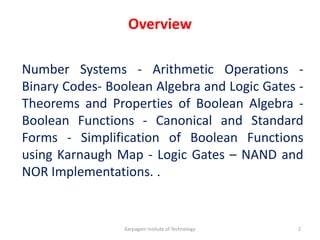
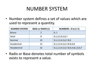
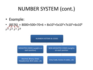
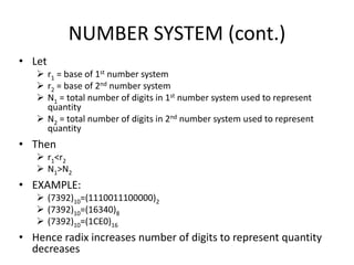
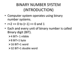
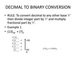
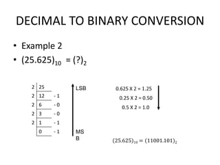
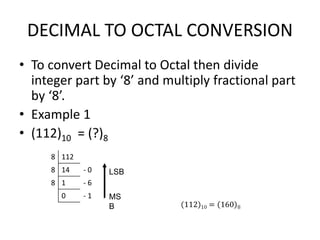
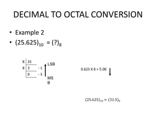
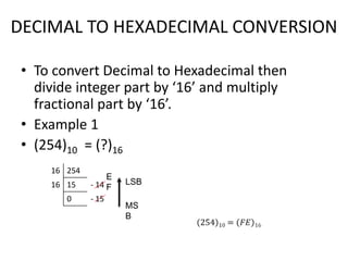
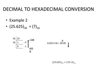
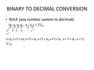
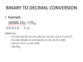
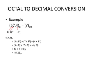
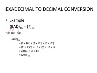
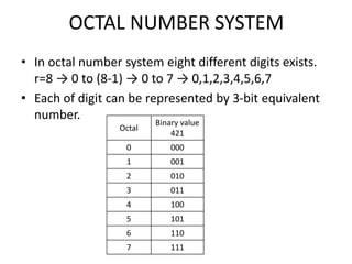
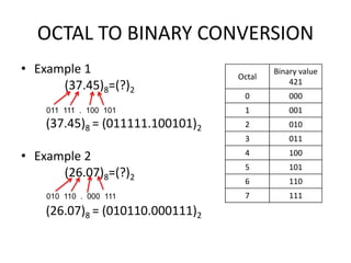
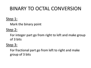
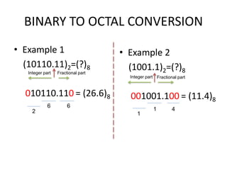
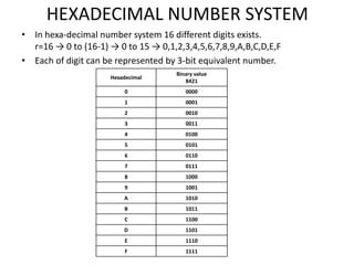
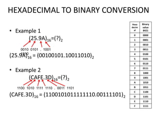
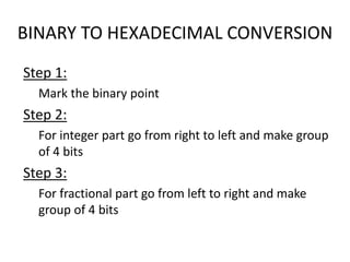
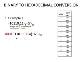
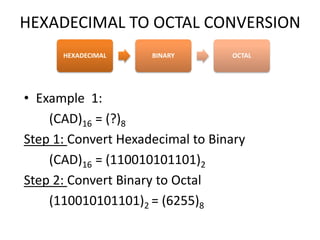
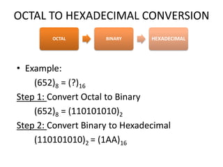
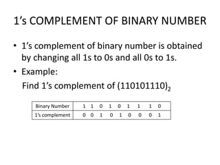
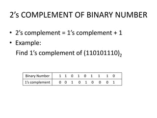
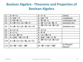
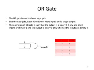
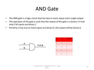
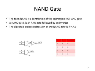
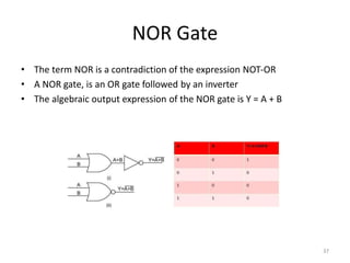
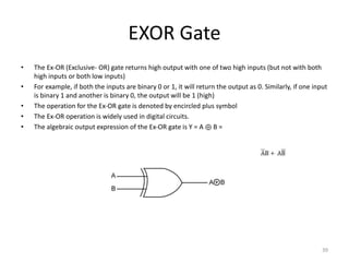
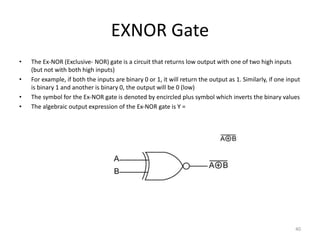
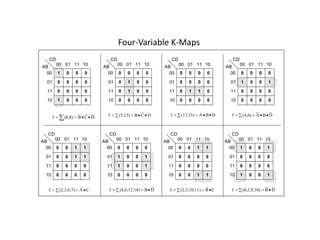
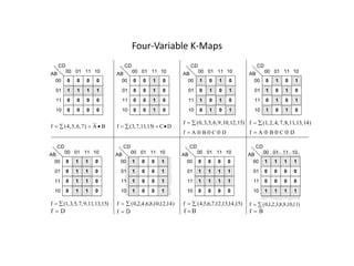
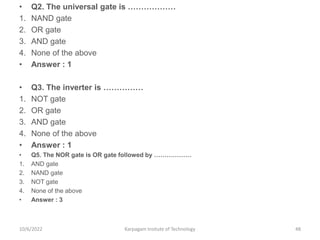
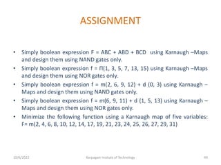
1
NUMBER SYSTEMS &
BOOLEAN ALGEBRA
Presented By:
Veera Boopathy.E
Assistant Professor,
Department of ECE,
Karpagam Institute of Technology,
Coimbatore.
Overview
Number Systems - Arithmetic Operations -
Binary Codes- Boolean Algebra and Logic Gates -
Theorems and Properties of Boolean Algebra -
Boolean Functions - Canonical and Standard
Forms - Simplification of Boolean Functions
using Karnaugh Map - Logic Gates – NAND and
NOR Implementations. .
Karpagam Insitute of Technology 2
NUMBER SYSTEM
• Number system defines a set of values which are
used to represent a quantity.
• Radix or Base denotes total number of symbols
exists to represent a value.
NUMBER SYSTEM BASE or RADIX (r) NUMBERS : 0 to (r-1)
Binary 2 0, 1
Octal 8 0,1,2,3,4,5,6,7
Decimal 10 0,1,2,3,4,5,6,7,8,9
Duodecimal 12 0,1,2,3,4,5,6,7,8,9,A,B
Hexadecimal 16 0,1,2,3,4,5,6,7,8,9,A,B,C,D,E,F
NUMBER SYSTEM (cont.)
NUMBER SYSTEMS & CODES
WEIGHTED CODES (weights on
each position)
Decimal, Binary, Octal,
Hexadecimal, BCD codes…etc
NON-WEIGHTED CODES (weights
on each position
Grey Code, Excess-3 codes,..etc
NUMBER SYSTEM (cont.)
• Let
 r1 = base of 1st number system
 r2 = base of 2nd number system
 N1 = total number of digits in 1st number system used to represent
quantity
 N2 = total number of digits in 2nd number system used to represent
quantity
• Then
 r1<r2
 N1>N2
• EXAMPLE:
 (7392)10=(1110011100000)2
 (7392)10=(16340)8
 (7392)10=(1CE0)16
• Hence radix increases number of digits to represent quantity
decreases
BINARY NUMBER SYSTEM
(INTRODUCTION)
• Computer system operates using binary
number systems.
• r=2 => 0 to (r-1) => 0 and 1
• Each and every unit of binary number is called
Binary digit (BIT).
4 BIT= 1 nibble
8 BIT=1 byte
16 BIT=1 word
32 BIT=1 double word
DECIMAL TO BINARY CONVERSION
• RULE: To convert decimal to any other base ‘r’
then divide integer part by ‘r’ and multiply
fractional part by ‘r’.
• Example 1
• (13)10 = (?)2
2 13
2 6 - 1
2 3 - 0
2 1 - 1
0 - 1
LSB
MS
B
DECIMAL TO BINARY CONVERSION
• Example 2
• (25.625)10 = (?)2
2 25
2 12 - 1
2 6 - 0
2 3 - 0
2 1 - 1
0 - 1
LSB
MS
B
0.25 X 2 = 0.50
0.5 X 2 = 1.0
DECIMAL TO OCTAL CONVERSION
• To convert Decimal to Octal then divide
integer part by ‘8’ and multiply fractional part
by ‘8’.
• Example 1
• (112)10 = (?)8
8 112
8 14 - 0
8 1 - 6
0 - 1
LSB
MS
B
DECIMAL TO OCTAL CONVERSION
• Example 2
• (25.625)10 = (?)8
8 25
8 3 - 1
0 - 3
LSB
MS
B
• To convert Decimal to Hexadecimal then
divide integer part by ‘16’ and multiply
fractional part by ‘16’.
• Example 1
• (254)10 = (?)16
16 254
16 15 - 14
0 - 15
LSB
MS
B
DECIMAL TO HEXADECIMAL CONVERSION
E
F
DECIMAL TO HEXADECIMAL CONVERSION
• Example 2
• (25.625)10 = (?)16
16 25
16 1 - 9
0 - 1
LSB
MS
B
A
BINARY TO DECIMAL CONVERSION
• RULE (any number system to decimal):
(a3 a2 a1 a0 . a-1 a-2)r
= (?)10
={ (a3 x r3) + (a2 x r2) + (a1 x r1) + (a0 x r0) + (a-1 x r-1) + (a-2 x r-2) }
=( )10
r3 r2 r1 r0 r-1
r-2
BINARY TO DECIMAL CONVERSION
• Example
(10101.11)2 = (?)10
(10101.11)2
= (1 x 24) + (0 x 23) + (1 x 22) + (0 x 21) + (1 x 20) + (1 x 2-1) + (1 x 2-2)
= (1 x 16) + (0 x 8) + (1 x 4) + (0 x 2) + (1 x 1) + (1 /2) + (1/4)
= 16 + 0 + 4 + 0 + 1 + 0.5 + 0.25
= (21.75)10
24 23 22 21 20 2-1 2-2
OCTAL TO DECIMAL CONVERSION
• Example
(57.4)8 = (?)10
(57.4)8
= (5 x 81) + (7 x 80) + (4 x 8-1)
= (5 x 8) + (7 x 1) + (4 / 8)
= 40 + 7 + 0.5
= (47.5)10
81 80 8-1
HEXADECIMAL TO DECIMAL CONVERSION
• Example
(BAD)16 = (?)10
(BAD)16
= (B x 162) + (A x 161) + (D x 160)
= (11 x 256) + (10 x 16) + (13 x 1)
= 2816 + 160 + 13
= (2989)10
162 161 160
OCTAL NUMBER SYSTEM
• In octal number system eight different digits exists.
r=8 → 0 to (8-1) → 0 to 7 → 0,1,2,3,4,5,6,7
• Each of digit can be represented by 3-bit equivalent
number.
Octal
Binary value
421
0 000
1 001
2 010
3 011
4 100
5 101
6 110
7 111
OCTAL TO BINARY CONVERSION
• Example 1
(37.45)8=(?)2
(37.45)8 = (011111.100101)2
• Example 2
(26.07)8=(?)2
(26.07)8 = (010110.000111)2
011 111 . 100 101
010 110 . 000 111
Octal
Binary value
421
0 000
1 001
2 010
3 011
4 100
5 101
6 110
7 111
BINARY TO OCTAL CONVERSION
Step 1:
Mark the binary point
Step 2:
For integer part go from right to left and make group
of 3 bits
Step 3:
For fractional part go from left to right and make
group of 3 bits
BINARY TO OCTAL CONVERSION
• Example 1
(10110.11)2=(?)8
010110.110 = (26.6)8
Integer part Fractional part
6
2
6
• Example 2
(1001.1)2=(?)8
001001.100 = (11.4)8
Integer part Fractional part
1
1 4
HEXADECIMAL NUMBER SYSTEM
• In hexa-decimal number system 16 different digits exists.
r=16 → 0 to (16-1) → 0 to 15 → 0,1,2,3,4,5,6,7,8,9,A,B,C,D,E,F
• Each of digit can be represented by 3-bit equivalent number.
Hexadecimal
Binary value
8421
0 0000
1 0001
2 0010
3 0011
4 0100
5 0101
6 0110
7 0111
8 1000
9 1001
A 1010
B 1011
C 1100
D 1101
E 1110
F 1111
HEXADECIMAL TO BINARY CONVERSION
• Example 1
(25.9A)16=(?)2
(25.9A)16 = (00100101.10011010)2
• Example 2
(CAFE.3D)16=(?)2
(CAFE.3D)16 = (1100101011111110.00111101)2
0010 0101 . 1001
1010
1100 1010 1111 1110 . 0011 1101
Hexa
decim
al
Binary
value
8421
0 0000
1 0001
2 0010
3 0011
4 0100
5 0101
6 0110
7 0111
8 1000
9 1001
A 1010
B 1011
C 1100
D 1101
E 1110
F 1111
BINARY TO HEXADECIMAL CONVERSION
Step 1:
Mark the binary point
Step 2:
For integer part go from right to left and make group
of 4 bits
Step 3:
For fractional part go from left to right and make
group of 4 bits
BINARY TO HEXADECIMAL CONVERSION
• Example 1
(10110.11)2=(?)16
00010110.1100 =(16.C)16
Integer part Fractional part
6
1
C
Hexa
decimal
Binary
value
8421
0 0000
1 0001
2 0010
3 0011
4 0100
5 0101
6 0110
7 0111
8 1000
9 1001
A 1010
B 1011
C 1100
D 1101
E 1110
F 1111
HEXADECIMAL TO OCTAL CONVERSION
• Example 1:
(CAD)16 = (?)8
Step 1: Convert Hexadecimal to Binary
(CAD)16 = (110010101101)2
Step 2: Convert Binary to Octal
(110010101101)2 = (6255)8
HEXADECIMAL BINARY OCTAL
OCTAL TO HEXADECIMAL CONVERSION
• Example:
(652)8 = (?)16
Step 1: Convert Octal to Binary
(652)8 = (110101010)2
Step 2: Convert Binary to Hexadecimal
(110101010)2 = (1AA)16
OCTAL BINARY HEXADECIMAL
1’s COMPLEMENT OF BINARY NUMBER
• 1’s complement of binary number is obtained
by changing all 1s to 0s and all 0s to 1s.
• Example:
Find 1’s complement of (110101110)2
Binary Number 1 1 0 1 0 1 1 1 0
1’s complement 0 0 1 0 1 0 0 0 1
2’s COMPLEMENT OF BINARY NUMBER
• 2’s complement = 1’s complement + 1
• Example:
Find 1’s complement of (110101110)2
Binary Number 1 1 0 1 0 1 1 1 0
1’s complement 0 0 1 0 1 0 0 0 1
Boolean Algebra - Theorems and Properties of
Boolean Algebra
10/6/2022 Karpagam Insitute of Technology 29
BOOLEAN POSTULATES AND LAWS:
10/6/2022 Karpagam Insitute of Technology 30
T1 : Commutative Law
(a) A + B = B + A
(b) A B = B A
T2 : Associate Law
(a) (A + B) + C = A + (B + C)
(b) (A B) C = A (B C)
T3 : Distributive Law
(a) A (B + C) = A B + A C
(b) A + (B C) = (A + B) (A + C)
T4 : Identity Law
(a) A + A = A
(b) A A = A
Logic Circuits
• A collection of individual logic gates connect with each other and
produce a logic design known as a Logic Circuit
• The following are the types of logic circuits:
– Decision making
– Memory
– A gate has two or more binary inputs and single output.
Logic Circuits
Basic Logic Gates
• The following are the three basic gates:
– NOT
– AND
– OR
– Each logic gate performs a different logic function.
You can derive logical function or any Boolean or
logic expression by combining these three gates.
NOT Gate
• The simplest form of a digital logic circuit is the inverter or the NOT
gate
• It consists of one input and one output and the input can only be
binary numbers namely; 0 and 1
the truth table for NOT Gate:
33
OR Gate
• The OR gate is another basic logic gate
• Like the AND gate, it can have two or more inputs and a single output
• The operation of OR gate is such that the output is a binary 1 if any one or all
inputs are binary 1 and the output is binary 0 only when all the inputs are binary 0
34
AND Gate
• The AND gate is a logic circuit that has two or more inputs and a single output
• The operation of the gate is such that the output of the gate is a binary 1 if and
only if all inputs are binary 1
• Similarly, if any one or more inputs are binary 0, the output will be binary 0.
Fundamentals of Digital Electronics - Logic
Gates
35
NAND Gate
• The term NAND is a contraction of the expression NOT-AND gate
• A NAND gate, is an AND gate followed by an inverter
• The algebraic output expression of the NAND gate is Y = A.B
36
NOR Gate
• The term NOR is a contradiction of the expression NOT-OR
• A NOR gate, is an OR gate followed by an inverter
• The algebraic output expression of the NOR gate is Y = A + B
37
EX-OR and EX-NOR Gates
• EX-OR and EX-NOR are digital logic circuits
that may use two or more inputs
• EX-NOR gate returns the output opposite to
EX-OR gate
• EX-OR and EX-NOR gates are also denoted by
XOR and XNOR respectively.
38
EXOR Gate
• The Ex-OR (Exclusive- OR) gate returns high output with one of two high inputs (but not with both
high inputs or both low inputs)
• For example, if both the inputs are binary 0 or 1, it will return the output as 0. Similarly, if one input
is binary 1 and another is binary 0, the output will be 1 (high)
• The operation for the Ex-OR gate is denoted by encircled plus symbol
• The Ex-OR operation is widely used in digital circuits.
• The algebraic output expression of the Ex-OR gate is Y = A ⊕ B =
39
EXNOR Gate
• The Ex-NOR (Exclusive- NOR) gate is a circuit that returns low output with one of two high inputs
(but not with both high inputs)
• For example, if both the inputs are binary 0 or 1, it will return the output as 1. Similarly, if one input
is binary 1 and another is binary 0, the output will be 0 (low)
• The symbol for the Ex-NOR gate is denoted by encircled plus symbol which inverts the binary values
• The algebraic output expression of the Ex-NOR gate is Y =
40
Applications of Logic Gates
• The following are some of the applications of Logic
gates:
– Build complex systems that can be used to different fields
such as
• Genetic engineering,
• Nanotechnology,
• Industrial Fermentation,
• Metabolic engineering and
• Medicine
– Construct multiplexers, adders and multipliers.
– Perform several parallel logical operations
– Used for a simple house alarm or fire alarm or in the circuit
of automated machine manufacturing industry
41
Karnaugh Maps (K-Maps)
•A visual way to simplify logic
expressions
•It gives the most simplified form
of the expression
Rules to obtain the most simplified
expression
•Simplification of logic expression using Boolean algebra is awkward because:
–it lacks specific rules to predict the most suitable next step in the simplification
process
–it is difficult to determine whether the simplest form has been achieved.
•A Karnaugh map is a graphical method used to obtained the most simplified form of
an expression in a standard form (Sum-of-Products or Product-of-Sums).
•The simplest form of an expression is the one that has the minimum number of
terms with the least number of literals (variables) in each term.
•By simplifying an expression to the one that uses the minimum number of terms, we
ensure that the function will be implemented with the minimum number of gates.
•By simplifying an expression to the one that uses the least number of literals for
each terms, we ensure that the function will be implemented with gates that have
the minimum number of inputs.
Three-Variable K-Maps
 
 C
B
(0,4)
f  
 B
A
(4,5)
f  
 B
(0,1,4,5)
f  
 A
(0,1,2,3)
f
BC
00
0
01
1
11 10
A
1 0 0 0
1 0 0 0
BC
00
0
01
1
11 10
A
0 0 0 0
1 1 0 0
BC
00
0
01
1
11 10
A
1 1 1 1
0 0 0 0
BC
00
0
01
1
11 10
A
1 1 0 0
1 1 0 0
 
 C
A
(0,4)
f  
 C
A
(4,6)
f  
 C
A
(0,2)
f  
 C
(0,2,4,6)
f
BC
00
0
01
1
11 10
A
0 1 1 0
0 0 0 0
BC
00
0
01
1
11 10
A
0 0 0 0
1 0 0 1
BC
00
0
01
1
11 10
A
1 0 0 1
1 0 0 1
BC
00
0
01
1
11 10
A
1 0 0 1
0 0 0 0
Four-Variable K-Maps
 


 D
C
B
(0,8)
f  


 D
C
B
(5,13)
f  


 D
B
A
(13,15)
f  


 D
B
A
(4,6)
f
 

 C
A
(2,3,6,7)
f  

 D
B
)
(4,6,12,14
f  

 C
B
)
(2,3,10,11
f  

 D
B
(0,2,8,10)
f
CD
00
00
01
01
11
11
10
10
AB
1 0 0 0
0 0 0 0
0 0 0 0
1 0 0 0
CD
00
00
01
01
11
11
10
10
AB
0 0 0 0
0 1 0 0
0 1 0 0
0 0 0 0
CD
00
00
01
01
11
11
10
10
AB
0 0 0 0
0 0 0 0
0 1 1 0
0 0 0 0
CD
00
00
01
01
11
11
10
10
AB
0 0 0 0
1 0 0 1
0 0 0 0
0 0 0 0
CD
00
00
01
01
11
11
10
10
AB
0 0 1 1
0 0 1 1
0 0 0 0
0 0 0 0
CD
00
00
01
01
11
11
10
10
AB
0 0 0 0
1 0 0 1
1 0 0 1
0 0 0 0
CD
00
00
01
01
11
11
10
10
AB
0 0 1 1
0 0 0 0
0 0 0 0
0 0 1 1
CD
00
00
01
01
11
11
10
10
AB
1 0 0 1
0 0 0 0
0 0 0 0
1 0 0 1
Four-Variable K-Maps
CD
00
00
01
01
11
11
10
10
AB
0 0 0 0
1 1 1 1
0 0 0 0
0 0 0 0
CD
00
00
01
01
11
11
10
10
AB
0 0 1 0
0 0 1 0
0 0 1 0
0 0 1 0
CD
00
00
01
01
11
11
10
10
AB
1 0 1 0
0 1 0 1
1 0 1 0
0 1 0 1
CD
00
00
01
01
11
11
10
10
AB
0 1 0 1
1 0 1 0
0 1 0 1
1 0 1 0
CD
00
00
01
01
11
11
10
10
AB
0 1 1 0
0 1 1 0
0 1 1 0
0 1 1 0
CD
00
00
01
01
11
11
10
10
AB
1 0 0 1
1 0 0 1
1 0 0 1
1 0 0 1
CD
00
00
01
01
11
11
10
10
AB
0 0 0 0
1 1 1 1
1 1 1 1
0 0 0 0
CD
00
00
01
01
11
11
10
10
AB
1 1 1 1
0 0 0 0
0 0 0 0
1 1 1 1
f (4,5,6,7) A B
  
 f (3,7,11,15) C D
  

f (0,3,5,6,9,10,12,15)
  f (1,2,4,7,8,11,13,14)
 
f A B C D
    f A B C D
   
f (1,3,5,7,9,11,13,15)
  f (0,2,4,6,8,10,12,14)
  f (4,5,6,7,12,13,14,15)
  f (0,1,2,3,8,9,10,11)
 
f D
 f D
 f B
 f B

Quiz – Test your knowledge
• Q1. The binary number 10101 is
equivalent to decimal number …………..
1.19
2.12
3.27
4.21
• Answer : 4
10/6/2022 Karpagam Insitute of Technology 47
• Q2. The universal gate is ………………
1. NAND gate
2. OR gate
3. AND gate
4. None of the above
• Answer : 1
• Q3. The inverter is ……………
1. NOT gate
2. OR gate
3. AND gate
4. None of the above
• Answer : 1
• Q5. The NOR gate is OR gate followed by ………………
1. AND gate
2. NAND gate
3. NOT gate
4. None of the above
• Answer : 3
10/6/2022 Karpagam Insitute of Technology 48
ASSIGNMENT
• Simply boolean expression F = ABC + ABD + BCD using Karnaugh –Maps
and design them using NAND gates only.
• Simply boolean expression f = Π(1, 3, 5, 7, 13, 15) using Karnaugh –Maps
and design them using NOR gates only.
• Simply boolean expression f = m(2, 6, 9, 12) + d (0, 3) using Karnaugh –
Maps and design them using NAND gates only.
• Simply boolean expression f = m(6, 9, 11) + d (1, 5, 13) using Karnaugh –
Maps and design them using NOR gates only.
• Minimize the following function using a Karnaugh map of five variables:
F= m(2, 4, 6, 8, 10, 12, 14, 17, 19, 21, 23, 24, 25, 26, 27, 29, 31)
10/6/2022 Karpagam Insitute of Technology 49

Number_Systems_and_Boolean_Algebra.ppt

  • 1.
    1 NUMBER SYSTEMS & BOOLEANALGEBRA Presented By: Veera Boopathy.E Assistant Professor, Department of ECE, Karpagam Institute of Technology, Coimbatore.
  • 2.
    Overview Number Systems -Arithmetic Operations - Binary Codes- Boolean Algebra and Logic Gates - Theorems and Properties of Boolean Algebra - Boolean Functions - Canonical and Standard Forms - Simplification of Boolean Functions using Karnaugh Map - Logic Gates – NAND and NOR Implementations. . Karpagam Insitute of Technology 2
  • 3.
    NUMBER SYSTEM • Numbersystem defines a set of values which are used to represent a quantity. • Radix or Base denotes total number of symbols exists to represent a value. NUMBER SYSTEM BASE or RADIX (r) NUMBERS : 0 to (r-1) Binary 2 0, 1 Octal 8 0,1,2,3,4,5,6,7 Decimal 10 0,1,2,3,4,5,6,7,8,9 Duodecimal 12 0,1,2,3,4,5,6,7,8,9,A,B Hexadecimal 16 0,1,2,3,4,5,6,7,8,9,A,B,C,D,E,F
  • 4.
    NUMBER SYSTEM (cont.) NUMBERSYSTEMS & CODES WEIGHTED CODES (weights on each position) Decimal, Binary, Octal, Hexadecimal, BCD codes…etc NON-WEIGHTED CODES (weights on each position Grey Code, Excess-3 codes,..etc
  • 5.
    NUMBER SYSTEM (cont.) •Let  r1 = base of 1st number system  r2 = base of 2nd number system  N1 = total number of digits in 1st number system used to represent quantity  N2 = total number of digits in 2nd number system used to represent quantity • Then  r1<r2  N1>N2 • EXAMPLE:  (7392)10=(1110011100000)2  (7392)10=(16340)8  (7392)10=(1CE0)16 • Hence radix increases number of digits to represent quantity decreases
  • 6.
    BINARY NUMBER SYSTEM (INTRODUCTION) •Computer system operates using binary number systems. • r=2 => 0 to (r-1) => 0 and 1 • Each and every unit of binary number is called Binary digit (BIT). 4 BIT= 1 nibble 8 BIT=1 byte 16 BIT=1 word 32 BIT=1 double word
  • 7.
    DECIMAL TO BINARYCONVERSION • RULE: To convert decimal to any other base ‘r’ then divide integer part by ‘r’ and multiply fractional part by ‘r’. • Example 1 • (13)10 = (?)2 2 13 2 6 - 1 2 3 - 0 2 1 - 1 0 - 1 LSB MS B
  • 8.
    DECIMAL TO BINARYCONVERSION • Example 2 • (25.625)10 = (?)2 2 25 2 12 - 1 2 6 - 0 2 3 - 0 2 1 - 1 0 - 1 LSB MS B 0.25 X 2 = 0.50 0.5 X 2 = 1.0
  • 9.
    DECIMAL TO OCTALCONVERSION • To convert Decimal to Octal then divide integer part by ‘8’ and multiply fractional part by ‘8’. • Example 1 • (112)10 = (?)8 8 112 8 14 - 0 8 1 - 6 0 - 1 LSB MS B
  • 10.
    DECIMAL TO OCTALCONVERSION • Example 2 • (25.625)10 = (?)8 8 25 8 3 - 1 0 - 3 LSB MS B
  • 11.
    • To convertDecimal to Hexadecimal then divide integer part by ‘16’ and multiply fractional part by ‘16’. • Example 1 • (254)10 = (?)16 16 254 16 15 - 14 0 - 15 LSB MS B DECIMAL TO HEXADECIMAL CONVERSION E F
  • 12.
    DECIMAL TO HEXADECIMALCONVERSION • Example 2 • (25.625)10 = (?)16 16 25 16 1 - 9 0 - 1 LSB MS B A
  • 13.
    BINARY TO DECIMALCONVERSION • RULE (any number system to decimal): (a3 a2 a1 a0 . a-1 a-2)r = (?)10 ={ (a3 x r3) + (a2 x r2) + (a1 x r1) + (a0 x r0) + (a-1 x r-1) + (a-2 x r-2) } =( )10 r3 r2 r1 r0 r-1 r-2
  • 14.
    BINARY TO DECIMALCONVERSION • Example (10101.11)2 = (?)10 (10101.11)2 = (1 x 24) + (0 x 23) + (1 x 22) + (0 x 21) + (1 x 20) + (1 x 2-1) + (1 x 2-2) = (1 x 16) + (0 x 8) + (1 x 4) + (0 x 2) + (1 x 1) + (1 /2) + (1/4) = 16 + 0 + 4 + 0 + 1 + 0.5 + 0.25 = (21.75)10 24 23 22 21 20 2-1 2-2
  • 15.
    OCTAL TO DECIMALCONVERSION • Example (57.4)8 = (?)10 (57.4)8 = (5 x 81) + (7 x 80) + (4 x 8-1) = (5 x 8) + (7 x 1) + (4 / 8) = 40 + 7 + 0.5 = (47.5)10 81 80 8-1
  • 16.
    HEXADECIMAL TO DECIMALCONVERSION • Example (BAD)16 = (?)10 (BAD)16 = (B x 162) + (A x 161) + (D x 160) = (11 x 256) + (10 x 16) + (13 x 1) = 2816 + 160 + 13 = (2989)10 162 161 160
  • 17.
    OCTAL NUMBER SYSTEM •In octal number system eight different digits exists. r=8 → 0 to (8-1) → 0 to 7 → 0,1,2,3,4,5,6,7 • Each of digit can be represented by 3-bit equivalent number. Octal Binary value 421 0 000 1 001 2 010 3 011 4 100 5 101 6 110 7 111
  • 18.
    OCTAL TO BINARYCONVERSION • Example 1 (37.45)8=(?)2 (37.45)8 = (011111.100101)2 • Example 2 (26.07)8=(?)2 (26.07)8 = (010110.000111)2 011 111 . 100 101 010 110 . 000 111 Octal Binary value 421 0 000 1 001 2 010 3 011 4 100 5 101 6 110 7 111
  • 19.
    BINARY TO OCTALCONVERSION Step 1: Mark the binary point Step 2: For integer part go from right to left and make group of 3 bits Step 3: For fractional part go from left to right and make group of 3 bits
  • 20.
    BINARY TO OCTALCONVERSION • Example 1 (10110.11)2=(?)8 010110.110 = (26.6)8 Integer part Fractional part 6 2 6 • Example 2 (1001.1)2=(?)8 001001.100 = (11.4)8 Integer part Fractional part 1 1 4
  • 21.
    HEXADECIMAL NUMBER SYSTEM •In hexa-decimal number system 16 different digits exists. r=16 → 0 to (16-1) → 0 to 15 → 0,1,2,3,4,5,6,7,8,9,A,B,C,D,E,F • Each of digit can be represented by 3-bit equivalent number. Hexadecimal Binary value 8421 0 0000 1 0001 2 0010 3 0011 4 0100 5 0101 6 0110 7 0111 8 1000 9 1001 A 1010 B 1011 C 1100 D 1101 E 1110 F 1111
  • 22.
    HEXADECIMAL TO BINARYCONVERSION • Example 1 (25.9A)16=(?)2 (25.9A)16 = (00100101.10011010)2 • Example 2 (CAFE.3D)16=(?)2 (CAFE.3D)16 = (1100101011111110.00111101)2 0010 0101 . 1001 1010 1100 1010 1111 1110 . 0011 1101 Hexa decim al Binary value 8421 0 0000 1 0001 2 0010 3 0011 4 0100 5 0101 6 0110 7 0111 8 1000 9 1001 A 1010 B 1011 C 1100 D 1101 E 1110 F 1111
  • 23.
    BINARY TO HEXADECIMALCONVERSION Step 1: Mark the binary point Step 2: For integer part go from right to left and make group of 4 bits Step 3: For fractional part go from left to right and make group of 4 bits
  • 24.
    BINARY TO HEXADECIMALCONVERSION • Example 1 (10110.11)2=(?)16 00010110.1100 =(16.C)16 Integer part Fractional part 6 1 C Hexa decimal Binary value 8421 0 0000 1 0001 2 0010 3 0011 4 0100 5 0101 6 0110 7 0111 8 1000 9 1001 A 1010 B 1011 C 1100 D 1101 E 1110 F 1111
  • 25.
    HEXADECIMAL TO OCTALCONVERSION • Example 1: (CAD)16 = (?)8 Step 1: Convert Hexadecimal to Binary (CAD)16 = (110010101101)2 Step 2: Convert Binary to Octal (110010101101)2 = (6255)8 HEXADECIMAL BINARY OCTAL
  • 26.
    OCTAL TO HEXADECIMALCONVERSION • Example: (652)8 = (?)16 Step 1: Convert Octal to Binary (652)8 = (110101010)2 Step 2: Convert Binary to Hexadecimal (110101010)2 = (1AA)16 OCTAL BINARY HEXADECIMAL
  • 27.
    1’s COMPLEMENT OFBINARY NUMBER • 1’s complement of binary number is obtained by changing all 1s to 0s and all 0s to 1s. • Example: Find 1’s complement of (110101110)2 Binary Number 1 1 0 1 0 1 1 1 0 1’s complement 0 0 1 0 1 0 0 0 1
  • 28.
    2’s COMPLEMENT OFBINARY NUMBER • 2’s complement = 1’s complement + 1 • Example: Find 1’s complement of (110101110)2 Binary Number 1 1 0 1 0 1 1 1 0 1’s complement 0 0 1 0 1 0 0 0 1
  • 29.
    Boolean Algebra -Theorems and Properties of Boolean Algebra 10/6/2022 Karpagam Insitute of Technology 29
  • 30.
    BOOLEAN POSTULATES ANDLAWS: 10/6/2022 Karpagam Insitute of Technology 30 T1 : Commutative Law (a) A + B = B + A (b) A B = B A T2 : Associate Law (a) (A + B) + C = A + (B + C) (b) (A B) C = A (B C) T3 : Distributive Law (a) A (B + C) = A B + A C (b) A + (B C) = (A + B) (A + C) T4 : Identity Law (a) A + A = A (b) A A = A
  • 31.
    Logic Circuits • Acollection of individual logic gates connect with each other and produce a logic design known as a Logic Circuit • The following are the types of logic circuits: – Decision making – Memory – A gate has two or more binary inputs and single output. Logic Circuits
  • 32.
    Basic Logic Gates •The following are the three basic gates: – NOT – AND – OR – Each logic gate performs a different logic function. You can derive logical function or any Boolean or logic expression by combining these three gates.
  • 33.
    NOT Gate • Thesimplest form of a digital logic circuit is the inverter or the NOT gate • It consists of one input and one output and the input can only be binary numbers namely; 0 and 1 the truth table for NOT Gate: 33
  • 34.
    OR Gate • TheOR gate is another basic logic gate • Like the AND gate, it can have two or more inputs and a single output • The operation of OR gate is such that the output is a binary 1 if any one or all inputs are binary 1 and the output is binary 0 only when all the inputs are binary 0 34
  • 35.
    AND Gate • TheAND gate is a logic circuit that has two or more inputs and a single output • The operation of the gate is such that the output of the gate is a binary 1 if and only if all inputs are binary 1 • Similarly, if any one or more inputs are binary 0, the output will be binary 0. Fundamentals of Digital Electronics - Logic Gates 35
  • 36.
    NAND Gate • Theterm NAND is a contraction of the expression NOT-AND gate • A NAND gate, is an AND gate followed by an inverter • The algebraic output expression of the NAND gate is Y = A.B 36
  • 37.
    NOR Gate • Theterm NOR is a contradiction of the expression NOT-OR • A NOR gate, is an OR gate followed by an inverter • The algebraic output expression of the NOR gate is Y = A + B 37
  • 38.
    EX-OR and EX-NORGates • EX-OR and EX-NOR are digital logic circuits that may use two or more inputs • EX-NOR gate returns the output opposite to EX-OR gate • EX-OR and EX-NOR gates are also denoted by XOR and XNOR respectively. 38
  • 39.
    EXOR Gate • TheEx-OR (Exclusive- OR) gate returns high output with one of two high inputs (but not with both high inputs or both low inputs) • For example, if both the inputs are binary 0 or 1, it will return the output as 0. Similarly, if one input is binary 1 and another is binary 0, the output will be 1 (high) • The operation for the Ex-OR gate is denoted by encircled plus symbol • The Ex-OR operation is widely used in digital circuits. • The algebraic output expression of the Ex-OR gate is Y = A ⊕ B = 39
  • 40.
    EXNOR Gate • TheEx-NOR (Exclusive- NOR) gate is a circuit that returns low output with one of two high inputs (but not with both high inputs) • For example, if both the inputs are binary 0 or 1, it will return the output as 1. Similarly, if one input is binary 1 and another is binary 0, the output will be 0 (low) • The symbol for the Ex-NOR gate is denoted by encircled plus symbol which inverts the binary values • The algebraic output expression of the Ex-NOR gate is Y = 40
  • 41.
    Applications of LogicGates • The following are some of the applications of Logic gates: – Build complex systems that can be used to different fields such as • Genetic engineering, • Nanotechnology, • Industrial Fermentation, • Metabolic engineering and • Medicine – Construct multiplexers, adders and multipliers. – Perform several parallel logical operations – Used for a simple house alarm or fire alarm or in the circuit of automated machine manufacturing industry 41
  • 42.
    Karnaugh Maps (K-Maps) •Avisual way to simplify logic expressions •It gives the most simplified form of the expression
  • 43.
    Rules to obtainthe most simplified expression •Simplification of logic expression using Boolean algebra is awkward because: –it lacks specific rules to predict the most suitable next step in the simplification process –it is difficult to determine whether the simplest form has been achieved. •A Karnaugh map is a graphical method used to obtained the most simplified form of an expression in a standard form (Sum-of-Products or Product-of-Sums). •The simplest form of an expression is the one that has the minimum number of terms with the least number of literals (variables) in each term. •By simplifying an expression to the one that uses the minimum number of terms, we ensure that the function will be implemented with the minimum number of gates. •By simplifying an expression to the one that uses the least number of literals for each terms, we ensure that the function will be implemented with gates that have the minimum number of inputs.
  • 44.
    Three-Variable K-Maps   C B (0,4) f    B A (4,5) f    B (0,1,4,5) f    A (0,1,2,3) f BC 00 0 01 1 11 10 A 1 0 0 0 1 0 0 0 BC 00 0 01 1 11 10 A 0 0 0 0 1 1 0 0 BC 00 0 01 1 11 10 A 1 1 1 1 0 0 0 0 BC 00 0 01 1 11 10 A 1 1 0 0 1 1 0 0    C A (0,4) f    C A (4,6) f    C A (0,2) f    C (0,2,4,6) f BC 00 0 01 1 11 10 A 0 1 1 0 0 0 0 0 BC 00 0 01 1 11 10 A 0 0 0 0 1 0 0 1 BC 00 0 01 1 11 10 A 1 0 0 1 1 0 0 1 BC 00 0 01 1 11 10 A 1 0 0 1 0 0 0 0
  • 45.
    Four-Variable K-Maps     D C B (0,8) f      D C B (5,13) f      D B A (13,15) f      D B A (4,6) f     C A (2,3,6,7) f     D B ) (4,6,12,14 f     C B ) (2,3,10,11 f     D B (0,2,8,10) f CD 00 00 01 01 11 11 10 10 AB 1 0 0 0 0 0 0 0 0 0 0 0 1 0 0 0 CD 00 00 01 01 11 11 10 10 AB 0 0 0 0 0 1 0 0 0 1 0 0 0 0 0 0 CD 00 00 01 01 11 11 10 10 AB 0 0 0 0 0 0 0 0 0 1 1 0 0 0 0 0 CD 00 00 01 01 11 11 10 10 AB 0 0 0 0 1 0 0 1 0 0 0 0 0 0 0 0 CD 00 00 01 01 11 11 10 10 AB 0 0 1 1 0 0 1 1 0 0 0 0 0 0 0 0 CD 00 00 01 01 11 11 10 10 AB 0 0 0 0 1 0 0 1 1 0 0 1 0 0 0 0 CD 00 00 01 01 11 11 10 10 AB 0 0 1 1 0 0 0 0 0 0 0 0 0 0 1 1 CD 00 00 01 01 11 11 10 10 AB 1 0 0 1 0 0 0 0 0 0 0 0 1 0 0 1
  • 46.
    Four-Variable K-Maps CD 00 00 01 01 11 11 10 10 AB 0 00 0 1 1 1 1 0 0 0 0 0 0 0 0 CD 00 00 01 01 11 11 10 10 AB 0 0 1 0 0 0 1 0 0 0 1 0 0 0 1 0 CD 00 00 01 01 11 11 10 10 AB 1 0 1 0 0 1 0 1 1 0 1 0 0 1 0 1 CD 00 00 01 01 11 11 10 10 AB 0 1 0 1 1 0 1 0 0 1 0 1 1 0 1 0 CD 00 00 01 01 11 11 10 10 AB 0 1 1 0 0 1 1 0 0 1 1 0 0 1 1 0 CD 00 00 01 01 11 11 10 10 AB 1 0 0 1 1 0 0 1 1 0 0 1 1 0 0 1 CD 00 00 01 01 11 11 10 10 AB 0 0 0 0 1 1 1 1 1 1 1 1 0 0 0 0 CD 00 00 01 01 11 11 10 10 AB 1 1 1 1 0 0 0 0 0 0 0 0 1 1 1 1 f (4,5,6,7) A B     f (3,7,11,15) C D     f (0,3,5,6,9,10,12,15)   f (1,2,4,7,8,11,13,14)   f A B C D     f A B C D     f (1,3,5,7,9,11,13,15)   f (0,2,4,6,8,10,12,14)   f (4,5,6,7,12,13,14,15)   f (0,1,2,3,8,9,10,11)   f D  f D  f B  f B 
  • 47.
    Quiz – Testyour knowledge • Q1. The binary number 10101 is equivalent to decimal number ………….. 1.19 2.12 3.27 4.21 • Answer : 4 10/6/2022 Karpagam Insitute of Technology 47
  • 48.
    • Q2. Theuniversal gate is ……………… 1. NAND gate 2. OR gate 3. AND gate 4. None of the above • Answer : 1 • Q3. The inverter is …………… 1. NOT gate 2. OR gate 3. AND gate 4. None of the above • Answer : 1 • Q5. The NOR gate is OR gate followed by ……………… 1. AND gate 2. NAND gate 3. NOT gate 4. None of the above • Answer : 3 10/6/2022 Karpagam Insitute of Technology 48
  • 49.
    ASSIGNMENT • Simply booleanexpression F = ABC + ABD + BCD using Karnaugh –Maps and design them using NAND gates only. • Simply boolean expression f = Π(1, 3, 5, 7, 13, 15) using Karnaugh –Maps and design them using NOR gates only. • Simply boolean expression f = m(2, 6, 9, 12) + d (0, 3) using Karnaugh – Maps and design them using NAND gates only. • Simply boolean expression f = m(6, 9, 11) + d (1, 5, 13) using Karnaugh – Maps and design them using NOR gates only. • Minimize the following function using a Karnaugh map of five variables: F= m(2, 4, 6, 8, 10, 12, 14, 17, 19, 21, 23, 24, 25, 26, 27, 29, 31) 10/6/2022 Karpagam Insitute of Technology 49