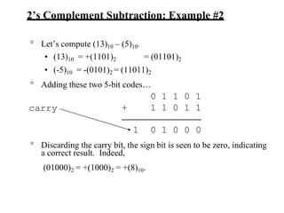
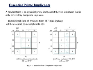
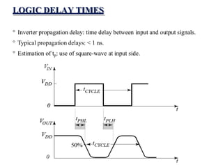
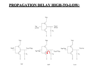
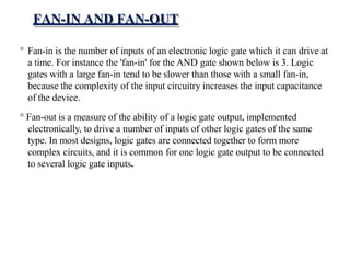
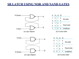
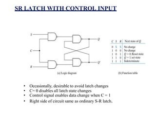
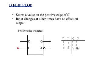
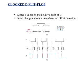
LECTURE NOTES ON
DIGITAL SYSTEM DESIGN
3rd semester
Branch-Electronics & Communication
Engineering
DEPT. OF ELECTRONICS AND COMMUNICATIONS ENGINEERING
AJAY KUMAR GARG ENGINEERING COLLEGE, GHAZIABAD
Prepared by:
Ms. Sulekha Saxena
Assistant Professor
ECE Department
AKGEC Ghaziabad
UNIT - 1
Logic Simplification and
Combinational logic design
Understanding Decimal Numbers
° Decimal numbers are made of decimal digits: (0,1,2,3,4,5,6,7,8,9)
° Decimal number representation:
• 8653 = 8x10³ + 6x10² + 5x101 + 3x100
° What about fractions?
• 97654.35 = 9x10⁴ + 7x10³ + 6x10² + 5x101 + 4x100 + 3x10⁻¹ + 5x10⁻²
• In formal notation -> (97654.35)10
° Why do we use 10 digits?
Understanding Binary Numbers
° Binary numbers are made of binary digits (bits):
• 0 and 1
° How many items does an binary number represent?
• (1011)2 = 1x23 + 0x22 + 1x21 + 1x20 = (11)10
° What about fractions?
• (110.10)2 = 1x22 + 1x21 + 0x20 + 1x2-1 + 0x2-2
° Groups of eight bits are called a byte
• (11001001) 2
° Groups of four bits are called a nibble.
• (1101) 2
Why Use Binary Numbers?
° Easy to represent 0 and 1 using
electrical values.
° Possible to tolerate noise.
° Easy to transmit data
° Easy to build binary circuits.
AND Gate
1
0
0
Conversion Between Number Bases
Decimal(base 10)
Octal(base 8)
Binary(base 2)
Hexadecimal
(base16)
° Learn to convert between bases.
° Conversion demonstrated in next slides
Convert an Integer from Decimal to Another Base
For each digit position:
1. Divide decimal number by the base (e.g. 2)
2. The remainder is the lowest-order digit
3. Repeat first two steps until no divisor remains.
Example for (13)10:
Integer Remainder
Quotient
13/2 = 6 + ½ a0 = 1
6/2 = 3 + 0 a1 = 0
3/2 = 1 + ½ a2 = 1
1/2 = 0 + ½ a3 = 1
Coefficient
Answer (13)10 = (a3 a2 a1 a0)2 = (1101)2
Convert an Fraction from Decimal to Another Base
For each digit position:
1. Multiply decimal number by the base (e.g. 2)
2. The integer is the highest-order digit
3. Repeat first two steps until fraction becomes zero.
Example for (0.625)10:
Integer
0.625 x 2 = 1 + 0.25 a-1 = 1
0.250 x 2 = 0 + 0.50 a-2 = 0
0.500 x 2 = 1 + 0 a-3 = 1
Fraction Coefficient
Answer (0.625)10 = (0.a-1 a-2 a-3 )2 = (0.101)2
The Growth of Binary Numbers
n 2n
0 20=1
1 21=2
2 22=4
3 23=8
4 24=16
5 25=32
6 26=64
7 27=128
n 2n
8 28=256
9 29=512
10 210=1024
11 211=2048
12 212=4096
20 220=1M
30 230=1G
40 240=1T
Mega
Giga
Tera
Binary Addition
1 1 1 1 1 1
1 1 1 1 0 1
+ 1 0 1 1 1
1 0 1 0 1 0 0
° Binary addition is very simple.
° This is best shown in an example of adding two binary
numbers…
carries
Binary Subtraction
° We can also perform subtraction (with borrows in place of
carries).
° Let’s subtract (10111)2 from (1001101)2…
1 10
0 10 10 0 0 10
1 0 0 1 1 0 1
1 0 1 1 1
-
1 1 0 1 1 0
borrows
Binary Multiplication
° Binary multiplication is much the same as decimal
multiplication, except that the multiplication operations are
much simpler…
1 0 1 1 1
X 1 0 1 0
0 0 0 0 0
1 0 1 1 1
0 0 0 0 0
1 0 1 1 1
1 1 1 0 0 1 1 0
Convert an Integer from Decimal to Octal
For each digit position:
1. Divide decimal number by the base (8)
2. The remainder is the lowest-order digit
3. Repeat first two steps until no divisor remains.
Example for (175)10:
Integer Remainder Coefficient
Quotient
175/8 = 21 + 7/8 a0 = 7
21/8 = 2 + 5/8 a1 = 5
2/8 = 0 + 2/8 a2 = 2
Answer (175)10 = (a2 a1 a0)2 = (257)8
Understanding Octal Numbers
° Octal numbers are made of octal digits: (0,1,2,3,4,5,6,7)
° Octal number representation:
• (4536)8 = 4x83 + 5x82 + 3x81 + 6x80 = (1362)10
° What about fractions?
• (465.27)8 = 4x82 + 6x81 + 5x80 + 2x8-1 + 7x8-2
° Octal numbers don’t use digits 8 or 9
Understanding Hexadecimal Numbers
° Hexadecimal numbers are made of 16 digits:
• (0,1,2,3,4,5,6,7,8,9,A, B, C, D, E, F)
° hex number representation:
• (3A9F)16 = 3x163 + 10x162 + 9x161 + 15x160 = 1499910
° What about fractions?
• (2D3.5)16 = 2x162 + 13x161 + 3x160 + 5x16-1 = 723.312510
° Note that each hexadecimal digit can be represented with four
bits.
• (1110) 2 = (E)16
° Groups of four bits are called a nibble.
• (1110) 2
Putting It All Together
° Binary, octal, and hexadecimal
similar
° Easy to build circuits to
operate on these
representations
° Possible to convert between
the three formats
Converting Between Base 16 and Base 2
3A9F16 = 0011 1010 1001 11112
3 A 9 F
° Determine 4-bit value for each hex digit
° Note that there are 24 = 16 different values of four bits
° Easier to read and write in hexadecimal.
° Representations are equivalent!
Converting Between Base 16 and Base 8
3A9F16 = 0011 1010 1001 11112
3 A 9 F
352378 = 011 101 010 011 1112
3 5 2 3 7
1. Convert from Base 16 to Base 2
2. Regroup bits into groups of three starting from right
3. Ignore leading zeros
4. Each group of three bits forms an octal digit.
How To Represent Signed Numbers
• Plus and minus sign used for decimal numbers: 25 (or
+25), -16, etc.
• For computers, desirable to represent everything as bits.
• Three types of signed binary number representations: signed
magnitude, 1’s complement, 2’s complement.
• In each case: left-most bit indicates sign: positive (0) or
negative (1).
Consider signed magnitude:
000011002 = 1210
Sign bit Magnitude
100011002 = -1210
Sign bit Magnitude
One’s Complement Representation
• The one’s complement of a binary number involves inverting
all bits.
• 1’s comp of 00110011 is 11001100
• 1’s comp of 10101010 is 01010101
• For an n bit number N the 1’s complement is (2n-1) – N.
• Called diminished radix complement by Mano since 1’s
complement for base (radix 2).
• To find negative of 1’s complement number take the 1’s
complement.
000011002 = 1210
Sign bit Magnitude
111100112 = -1210
Sign bit Magnitude
Two’s Complement Representation
• The two’s complement of a binary number involves inverting
all bits and adding 1.
• 2’s comp of 00110011 is 11001101
• 2’s comp of 10101010 is 01010110
• For an n bit number N the 2’s complement is (2n-1) – N + 1.
• Called radix complement by Mano since 2’s complement for
base (radix 2).
• To find negative of 2’s complement number take the 2’s
complement.
000011002 = 1210
Sign bit Magnitude
111101002 = -1210
Sign bit Magnitude
Two’s Complement
° Algorithm 1 – Simply complement each bit and then add 1 to the
result.
• Finding the 2’s complement of (01100101)2 and of its 2’s
complement…
N = 01100101 [N] = 10011011
10011010 01100100
+ 1
-
10011011
+ 1
01100101
° Algorithm 2 – Starting with the least significant bit, copy all of the bits
up to and including the first 1 bit and then complementing the
remaining bits.
• N
[N]
= 0 1 1 0 0 1 0 1
= 1 0 0 1 1 0 1 1
1’s Complement Addition
° Using 1’s complement numbers, adding numbers is easy.
° For example, suppose we wish to add +(1100)2 and +(0001)2.
° Let’s compute (12)10 + (1)10.
• (12)10 = +(1100)2
• (1)10 = +(0001)2
= 011002 in 1’s comp.
= 000012 in 1’s comp.
0 1 1 0 0
0 0 0 0 1
+
--------------
0 0 1 1 0 1
0
0 1 1 0 1
Add carry
Final
Result
Step 1: Add binary numbers
Step 2:Add carry to low-order bit
Add
1’s Complement Subtraction
° Using 1’s complement numbers, subtracting numbers is also easy.
° For example, suppose we wish to subtract +(0001)2 from +(1100)2.
° Let’s compute (12)10 - (1)10.
• (12)10 = +(1100)2 = 011002 in 1’s comp.
• (-1)10 = -(0001)2 = 111102 in 1’s comp. -
0 1 1 0 0
0 0 0 0 1
+
0 1 1 0 0
1 1 1 1 0
--------------
1 0 1 0 1 0
ry 1
0 1 0 1 1
Add car
Final
Result
Step 1: Take 1’s complement of 2nd operand
Step 2: Add binary numbers
Step 3: Add carry to low order bit
1’s comp
Add
2’s Complement Addition
° Using 2’s complement numbers, adding numbers is easy.
° For example, suppose we wish to add +(1100)2 and +(0001)2.
° Let’s compute (12)10 + (1)10.
• (12)10 = +(1100)2
• (1)10 = +(0001)2
= 011002 in 2’s comp.
= 000012 in 2’s comp.
0 1 1 0 0
0 0 0 0 1
+
--------------
0 0 1 1 0 1
Final
Result
Step 1: Add binary numbers
Step 2: Ignore carry bit
Add
Ignore
2’s Complement Subtraction
° Using 2’s complement numbers, follow steps for
subtraction
° For example, suppose we wish to subtract +(0001)2 from
+(1100)2.
° Let’s compute (12)10 - (1)10.
• (12)10 = +(1100)2
• (-1)10 = -(0001)2
= 011002 in 2’s comp.
= 111112 in 2’s comp.
-
0 1 1 0 0
0 0 0 0 1
--------------
+
0 1 1 0 0
1 1 1 1 1
--------------
1 0 1 0 1 1
Final
Result
Step 1: Take 2’s complement of 2nd operand
Step 2: Add binary numbers
Step 3: Ignore carry bit
2’s comp
Add
Ignore
Carry
2’s Complement Subtraction: Example #2
0 1 1 0 1
+ 1 1 0 1 1
1 0 1 0 0 0
° Let’s compute (13)10 – (5)10.
• (13)10 = +(1101)2 = (01101)2
• (-5)10 = -(0101)2 = (11011)2
° Adding these two 5-bit codes…
carry
° Discarding the carry bit, the sign bit is seen to be zero, indicating
a correct result. Indeed,
(01000)2 = +(1000)2 = +(8)10.
2’s Complement Subtraction: Example #3
° Let’s compute (5)10 – (12)10.
• (-12)10 = -(1100)2 = (10100)2
• (5)10 = +(0101)2 = (00101)2
° Adding these two 5-bit codes…
0 0 1 0 1
° Here, there is no carry bit and the sign bit is 1. This
indicates a negative result, which is what we expect.
(11001)2 = -(7)10.
+ 1 0 1 0 0
1 1 0 0 1
Boolean Algebra
Overview
° Logic functions with 1’s and 0’s
• Building digital circuitry
° Truth tables
° Logic symbols and waveforms
° Boolean algebra
° Properties of Boolean Algebra
• Reducing functions
• Transforming functions
Digital Systems
° Analysis problem:
• Determine binary outputs for each combination of inputs
° Design problem: given a task, develop a circuit that
accomplishes the task
• Many possible implementation
• Try to develop “best” circuit based on some criterion (size,
power, performance, etc.)
.
.
.
.
Logic
Circuit
Inputs Outputs
Describing Circuit Functionality: Inverter
° Basic logic functions have symbols.
° The same functionality can be represented with truth tables.
• Truth table completely specifies outputs for all input combinations.
° The above circuit is an inverter.
• An input of 0 is inverted to a 1.
• An input of 1 is inverted to a 0.
A Y
0 1
1 0
Input Output
A Y
Symbol
Truth Table
The AND Gate
° This is an AND gate.
° So, if the two inputs signals
are asserted (high) the
output will also be asserted.
Otherwise, the output will
be deasserted (low).
A B Y
0 0 0
0 1 0
1 0 0
1 1 1
A
B
Y
Truth Table
The OR Gate
° This is an OR gate.
° So, if either of the two
input signals are
asserted, or both of
them are, the output
will be asserted.
A B Y
0 0 0
0 1 1
1 0 1
1 1 1
A
B
Y
Describing Circuit Functionality: Waveforms
° Waveforms provide another approach for representing functionality.
° Values are either high (logic 1) or low (logic 0).
° Can you create a truth table from the waveforms?
A B Y
0 0 0
0 1 0
1 0 0
1 1 1
AND Gate
Consider three-input gates
3 Input OR Gate
Ordering Boolean Functions
° How to interpret AB+C?
• Is it AB ORed with C ?
• Is it AANDed with B+C ?
° Order of precedence for Boolean algebra: AND before OR.
° Note that parentheses are needed here :
Boolean Algebra
° A Boolean algebra is defined as a closed algebraic system containing a
set K or two or more elements and the two operators, . and +.
° Useful for identifying and minimizing circuit functionality
° Identity elements
• a + 0 = a
• a . 1 = a
° 0 is the identity element for the + operation.
° 1 is the identity element for the . operation.
Commutativity and Associativity of the Operators
° The Commutative Property:
For every a and b in K,
• a + b = b + a
• a . b = b . a
° The Associative Property:
For every a, b, and c in K,
• a + (b + c) = (a + b) + c
• a . (b . c) = (a . b) . c
Distributivity of the Operators and Complements
° The Distributive Property:
For every a, b, and c in K,
• a + ( b . c ) = ( a + b ) . ( a + c )
• a . ( b + c ) = ( a . b ) + ( a . c )
° The Existence of the Complement:
For every a in K there exists a unique element called a’ (complement of
a) such that,
• a + a’= 1
• a . a’ = 0
° To simplify notation, the . operator is frequently omitted. When two
elements are written next to each other, the AND (.) operator is
implied…
• a + b . c = ( a + b ) . ( a + c )
• a + bc = ( a + b )( a + c )
Duality
° The principle of duality is an important concept. This says that if an
expression is valid in Boolean algebra, the dual of that expression is also
valid.
° To form the dual of an expression, replace all + operators with .
operators, all . operators with + operators, all ones with zeros, and all
zeros with ones.
° Form the dual of the expression
a + (bc) = (a + b)(a + c)
° Following the replacement rules…
a(b + c) = ab + ac
° Take care not to alter the location of the parentheses if they are present.
Involution
° This theorem states:
a’’= a
° Remember that aa’ = 0 and a+a’=1.
• Therefore, a’ is the complement of a and a is also the complement of
a’.
• As the complement of a’ is unique, it follows that a’’=a.
° Taking the double inverse of a value will give the initial value.
Absorption
° This theorem states:
a + ab = a a(a+b) = a
° To prove the first half of this theorem:
a + ab = a . 1 + ab
= a (1 + b)
= a (b + 1)
= a (1)
a + ab = a
DeMorgan’s Theorem
° A key theorem in simplifying Boolean algebra expression is
DeMorgan’s Theorem. It states:
(a + b)’ = a’b’ (ab)’ = a’ + b’
° Complement the expression
a(b + z(x + a’)) and simplify.
(a(b+z(x + a’)))’ = a’+ (b + z(x + a’))’
= a’+ b’(z(x + a’))’
= a’+ b’(z’+ (x + a’)’)
= a’+ b’(z’+ x’a’’)
= a’+ b’(z’+ x’a)
Summary
° Basic logic functions can be made from AND, OR, and NOT (invert)
functions
° The behavior of digital circuits can be represented with waveforms, truth
tables, or symbols
° Primitive gates can be combined to form larger circuits
° Boolean algebra defines how binary variables can be combined
° Rules for associativity, commutativity, and distribution are similar to
algebra
° DeMorgan’s rules are important.
• Will allow us to reduce circuit sizes.
More Logic Functions: NAND, NOR, XOR
Overview
° More 2-input logic gates (NAND, NOR, XOR)
° Extensions to 3-input gates
° Converting between sum-of-products and NANDs
• SOP to NANDs
• NANDs to SOP
° Converting between sum-of-products and NORs
• SOP to NORs
• NORs to SOP
° Positive and negative logic
• We use primarily positive logic in this course.
Logic functions of N variables
° Each truth table represents one possible function (e.g. AND, OR)
N
° If there are N inputs, there are 22
° For example, is N is 2 then there are 16 possible truth tables.
° So far, we have defined 2 of these functions
• 14 more are possible.
° Why consider new functions?
• Cheaper hardware, more flexibility.
x y G
0 0 0
0 1 0
1 0 0
1 1 1
The NAND Gate
° This is a NAND gate. It is a combination of an AND gate
followed by an inverter. Its truth table shows this…
° NAND gates have several interesting properties…
• NAND(a,a)=(aa)’ = a’ = NOT(a)
• NAND’(a,b)=(ab)’’ = ab = AND(a,b)
• NAND(a’,b’)=(a’b’)’ = a+b = OR(a,b) A B Y
0 0 1
0 1 1
1 0 1
1 1 0
A
B
Y
The NAND Gate
° These three properties show that a NAND gate with both of its
inputs driven by the same signal is equivalent to a NOT gate
° A NAND gate whose output is complemented is equivalent to an
AND gate, and a NAND gate with complemented inputs acts as an
OR gate.
° Therefore, we can use a NAND gate to implement all three of the
elementary operators (AND,OR,NOT).
° Therefore, ANY switching function can be constructed using only
NAND gates. Such a gate is said to be primitive or functionally
complete.
A
Y
A
B
Y
Y
A
B
NOT Gate
AND Gate
OR Gate
NAND Gates into Other Gates
(what are these circuits?)
The NOR Gate
° This is a NOR gate. It is a combination of an OR gate followed
by an inverter. It’s truth table shows this…
° NOR gates also have several
interesting properties…
• NOR(a,a)=(a+a)’ = a’ = NOT(a)
• NOR’(a,b)=(a+b)’’= a+b = OR(a,b)
• NOR(a’,b’)=(a’+b’)’= ab = AND(a,b)
A B Y
0 0 1
0 1 0
1 0 0
1 1 0
A
B
Y
Functionally Complete Gates
° Just like the NAND gate, the NOR gate is functionally
complete…any logic function can be implemented using just
NOR gates.
° Both NAND and NOR gates are very valuable as any design can
be realized using either one.
° It is easier to build an IC chip using all NAND or NOR gates
than to combine AND,OR, and NOT gates.
° NAND/NOR gates are typically faster at switching and cheaper
to produce.
NOT Gate
OR Gate
AND Gate
NOR Gates into Other Gates
(what are these circuits?)
Y
A
Y
A
B
A
B
Y
The XOR Gate (Exclusive-OR)
° This is a XOR gate.
° XOR gates assert their output
when exactly one of the inputs
is asserted, hence the name.
° The switching algebra symbol
for this operation is , i.e.
1  1 = 0 and 1  0 = 1.
A B Y
0 0 0
0 1 1
1 0 1
1 1 0
A
B
Y
The XNOR Gate
A
B
° This is a XNOR gate.
° This functions as an
exclusive-NOR gate, or
simply the complement of
the XOR gate.
° The switching algebra symbol
for this operation is , i.e.
1  1 = 1 and 1  0 = 0.
A B Y
0 0 1
0 1 0
1 0 0
1 1 1
Y
NOR Gate Equivalence
° NOR Symbol, Equivalent Circuit, Truth Table
DeMorgan’s Theorem
° A key theorem in simplifying Boolean algebra expression is DeMorgan’s
Theorem. It states:
(a + b)’ = a’b’ (ab)’= a’ + b’
° Complement the expression
a(b + z(x + a’)) and simplify.
(a(b+z(x + a’)))’ = a’+ (b + z(x + a’))’
= a’+ b’(z(x + a’))’
= a’+ b’(z’+ (x + a’)’)
= a’+ b’(z’+ x’a’’)
= a’+ b’(z’+ x’a)
Example
° Determine the output expression for the below circuit and
simplify it using DeMorgan’s Theorem
Universality of NAND and NOR gates
Universality of NOR gate
° Equivalent representations of the AND, OR, and
NOT gates
Interpretation of the two NAND gate symbols
Interpretation of the two OR gate symbols
Summary
° Basic logic functions can be made from NAND, and NOR functions
° The behavior of digital circuits can be represented with waveforms, truth
tables, or symbols
° Primitive gates can be combined to form larger circuits
° Boolean algebra defines how binary variables with NAND, NOR can be
combined
° DeMorgan’s rules are important.
• Allow conversion to NAND/NOR representations
More Boolean Algebra
Overview
° Expressing Boolean functions
° Relationships between algebraic equations, symbols, and truth tables
° Simplification of Boolean expressions
° Minterms and Maxterms
° AND-OR representations
• Product of sums
• Sum of products
Boolean Functions
° Boolean algebra deals with binary variables and logic
operations.
° Function results in binary 0 or 1
x y z F
0 0 0 0
0 0 1 0
0 1 0 0
0 1 1 0
1 0 0 1
1 0 1 0
1 1 0 1
1 1 1 1 F = x(y+z’)
x
z’
y
z y+z’ F = x(y+z’)
Boolean Functions
° Boolean algebra deals with binary variables and logic
operations.
° Function results in binary 0 or 1
x y z xy yz G
0 0 0 0 0 0
0 0 1 0 0 0
0 1 0 0 0 0
0 1 1 0 1 1
1 0 0 0 0 0
1 0 1 0 0 0
1 1 0 1 0 1
1 1 1 1 1 1
x
y
z
G = xy +yz
yz
xy
We will learn how to transition between equation,
symbols, and truth table.
Representation Conversion
° Need to transition between boolean expression, truth table,
and circuit (symbols).
° Converting between truth table and expression is easy.
° Converting between expression and circuit is easy.
° More difficult to convert to truth table.
Truth
Table
Circuit Boolean
Expression
Truth Table to Expression
x y z G
0 0 0 0
0 0 1 0
0 1 0 0
0 1 1 1
1 0 0 0
1 0 1 0
1 1 0 1
1 1 1 1
xyz + xyz’ + x’yz
° Converting a truth table to an expression
• Each row with output of 1 becomes a product term
• Sum product terms together.
Any Boolean Expression can be
represented in sum of products form!
Equivalent Representations of Circuits
° All three formats are equivalent
° Number of 1’s in truth table output column equals AND terms for
Sum-of-Products (SOP)
x y z
x y z G
0 0 0 0
0 0 1 0
0 1 0 0
0 1 1 1
1 0 0 0
1 0 1 0
1 1 0 1
1 1 1 1
G = xyz + xyz’ + x’yz
G
x x
x
x
x
x
x
x
x
Reducing Boolean Expressions
° Is this the smallest possible implementation of this
expression? No!
° Use Boolean Algebra rules to reduce complexity while
preserving functionality.
° Step 1: Use Theorum 1 (a + a = a)
• So xyz + xyz’ + x’yz = xyz + xyz + xyz’ + x’yz
° Step 2: Use distributive rule a(b + c) = ab + ac
• So xyz + xyz + xyz’ + x’yz = xy(z + z’) + yz(x + x’)
° Step 3: Use Postulate 3 (a + a’ = 1)
• So xy(z + z’) + yz(x + x’) = xy.1 + yz.1
° Step 4: Use Postulate 2 (a . 1 = a)
• So xy.1 + yz.1 = xy + yz = xyz + xyz’ + x’yz
G = xyz + xyz’ + x’yz
Reduced Hardware Implementation
° Reduced equation requires less hardware!
° Same function implemented!
y z
x
G = xyz + xyz’ + x’yz = xy + yz
x y z G
0 0 0 0
0 0 1 0
0 1 0 0
0 1 1 1
1 0 0 0
1 0 1 0
1 1 0 1
1 1 1 1
G
x x
x
x
Minterms and Maxterms
° Each variable in a Boolean expression is a literal
° Boolean variables can appear in normal (x) or complement
form (x’)
° Each AND combination of terms is a minterm
° Each OR combination of terms is a maxterm
For example:
Minterms
x y z Minterm
0 0 0 x’y’z’ m0
0
…
0 1 x’y’z m1
1
…
0 0 xy’z’ m4
1 1 1 xyz m7
For example:
Maxterms
x y z Maxterm
0 0 0 x+y+z M0
…
…
0 0 1 x+y+z’ M1
1 0 0 x’+y+z M4
1 1 1 x’+y’+z’ M7
Representing Functions with Minterms
x y z G
0 0 0 0
0 0 1 0
0 1 0 0
0 1 1 1
1 0 0 0
1 0 1 0
1 1 0 1
1 1 1 1
° Minterm number same as row position in truth table (starting
from top from 0)
° Shorthand way to represent functions
G = xyz + xyz’ + x’yz
G = m7 + m6 + m3 = Σ(3, 6, 7)
Complementing Functions
° Minterm number same as row position in truth table (starting from top
from 0)
° Shorthand way to represent functions
x y z G G’
0 0 0 0 1
0 0 1 0 1
0 1 0 0 1
0 1 1 1 0
1 0 0 0 1
1 0 1 0 1
1 1 0 1 0
1 1 1 1 0
G = xyz + xyz’ + x’yz
G’ = (xyz + xyz’ + x’yz)’ =
Can we find a simpler representation?
Complementing Functions
° Step 1: assign temporary names
• b + c -> z
• (a + z)’ = G’
° Step 2: Use DeMorgans’ Law
• (a + z)’ = a’ . z’
° Step 3: Resubstitute (b+c) for z
• a’ . z’ = a’ . (b + c)’
° Step 4: Use DeMorgans’ Law
• a’ . (b + c)’ = a’ . (b’. c’)
° Step 5: Associative rule
• a’ . (b’. c’) = a’ . b’ . c’
G = a + b + c
G’ = (a + b + c)’
G = a + b + c
G’ = a’ . b’ . c’ = a’b’c’
Complementation Example
° Find complement of F = x’z + yz
• F’= (x’z + yz)’
° DeMorgan’s
• F’ = (x’z)’(yz)’
° DeMorgan’s
• F’ = (x’’+z’)(y’+z’)
° Reduction -> eliminate double negation on x
• F’ = (x+z’)(y’+z’)
This format is called product of sums
Conversion Between Canonical Forms
x y z G
0 0 0 0
0 0 1 0
0 1 0 0
0 1 1 1
1 0 0 0
1 0 1 0
1 1 0 1
1 1 1 1
° Easy to convert between minterm and maxterm
representations
° For maxterm representation, select rows with 0’s
G = xyz + xyz’+ x’yz
G = m7 + m6 + m3 = Σ(3, 6, 7)
G = M0M1M2M4M5 = Π(0,1,2,4,5)
G = (x+y+z)(x+y+z’)(x+y’+z)(x’+y+z)(x’+y+z’)
Representation of Circuits
° All logic expressions can be represented in 2-level format
° Circuits can be reduced to minimal 2-level representation
° Sum of products representation most common in industry.
Summary
° Truth table, circuit, and boolean expression formats are
equivalent
° Easy to translate truth table to SOP and POS representation
° Boolean algebra rules can be used to reduce circuit size while
maintaining function
° All logic functions can be made from AND, OR, and NOT
° Easiest way to understand: Solve examples!
Minimization with Karnaugh Maps
Overview
° K-maps: an alternate approach to representing Boolean functions
° K-map representation can be used to minimize Boolean functions
° Easy conversion from truth table to K-map to minimized SOP
representation.
° Simple rules (steps) used to perform minimization
° Leads to minimized SOP representation.
• Much faster and more more efficient than previous minimization techniques with
Boolean algebra.
x y F
0 0 1
0 1 1
1 0 0
1 1 0
Karnaugh maps
° Alternate way of representing Boolean function
• All rows of truth table represented with a square
• Each square represents a minterm
° Easy to convert between truth table, K-map, and SOP
• Unoptimized form: number of 1’s in K-map equals number of minterms
(products) in SOP
• Optimized form: reduced number of minterms
0 1
x
y
0
1
1 1
0 0
y
0 1
x
y
0
1
x’y’ x’y
xy’ xy
x
F = Σ(m0,m1) = x’y + x’y’
Karnaugh Maps
° A Karnaugh map is a graphical tool for assisting in the general
simplification procedure.
° Two variable maps.
0 1
1 0
B
A 0 1
0
1
F=AB +A’B 0 1
1 1
B
A 0 1
A
0
1
° Three variable maps.
BC
0 1 0 1
1 1 1 1
00 01 11 10
F=AB’C’ +AB C +ABC +ABC  + A’B’C + A’BC’
+AB 
0 F=AB +AB
1
A B C F
0 0 0 0
0 0 1 1
0 1 0 1
0 1 1 0
1 0 0 1
1 0 1 1
1 1 0 1
1 1 1 1
+
Rules for K-Maps
 We can reduce functions by circling 1’s in the K-map
 Each circle represents minterm reduction
Following circling, we can deduce minimized and-or form.
Rules to consider
ÊEvery cell containing a 1 must be included at least once.
ËThe largest possible “power of 2 rectangle” must be enclosed.
Ì The 1’s must be enclosed in the smallest possible number of
rectangles.
Example
Karnaugh Maps
° A Karnaugh map is a graphical tool for assisting in the general
simplification procedure.
° Two variable maps.
0 1
1 0
B
A 0 1
0
1
F=AB +A’B 0
1 1
1
B
A 0 1
0
1
F=AB +AB +AB 
F=A+B
F=A+B C +BC 
A
1
0
1
° Three variable maps.
BC
1
1 1
0 1 0 1
00 01 11 10
F=AB’C’ +AB C +ABC +ABC  + A’B’C + A’BC’
Karnaugh maps
° Numbering scheme based on Gray–code
• e.g., 00, 01, 11, 10
• Only a single bit changes in code for adjacent map cells
• This is necessary to observe the variable transitions
C
AB
00
0
A
01 11 10
C 1
B
F(A,B,C) = m(0,4,5,7)= AC + B’C’
G(A,B,C) = A
0 0 1 1
0 0 1 1
C
A
1 0 0 1
0 0 1 1
C
B
B
A
More Karnaugh Map Examples
° Examples
0 1
0
1
a
b
0 1
0 1
ab
c 00 01 11 10
0
1
0
1
a
0 1
b
1 1
0 0
g = b'
ab
c 00 01 11 10
0
1
0 0 1 1
0 0 1 1
f = a
0 0 1 0
0 1 1 1
cout = ab + bc + ac
f = a
1. Circle the largest groups possible.
2. Group dimensions must be a power of 2.
3. Remember what circling means!
Application of Karnaugh Maps: The One-bit Adder
Adder
Cin
Cout
S
A
B
A B Cin S Cout
0 0 0 0 0
0 0 1 1 0
0 1 0 1 0
0 1 1 0 1
1 0 0 1 0
1 0 1 0 1
1 1 0 0 1
1 1 1 1 1
+
S =A
’B’Cin +A
’BCin’+A
’BCin +ABCin
Cout =A
’BCin +AB’Cin +ABCin’+ABCin
= A’BCin + ABCin + AB’Cin + ABCin + ABCin’ + ABCin
= (A
’+A)BCin + (B’+ B)ACin + (Cin’+ Cin)AB
= 1·BCin + 1·ACin + 1·AB
= BCin +ACin +AB
How to use a Karnaugh
Map instead of the
Algebraic simplification?
Application of Karnaugh Maps: The One-bit Adder
Adder
Cin
Cout
S
A
B
A B Cin S Cout
0 0 0 0 0
0 0 1 1 0
0 1 0 1 0
0 1 1 0 1
1 0 0 1 0
1 0 1 0 1
1 1 0 0 1
1 1 1 1 1
+
Now we have to cover all the 1s in the
Karnaugh Map using the largest
rectangles and as few rectangles
as we can.
A
B
Cin
Karnaugh Map for Cout
0 0 1 0
0 1 1 1
A
B
Cin
Karnaugh Map for Cout
0 0 1 0
0 1 1 1
Application of Karnaugh Maps: The One-bit Adder
Adder
Cin
Cout
S
A
B
A B Cin S Cout
0 0 0 0 0
0 0 1 1 0
0 1 0 1 0
0 1 1 0 1
1 0 0 1 0
1 0 1 0 1
1 1 0 0 1
1 1 1 1 1
+
Now we have to cover all the 1s in the
Karnaugh Map using the largest
rectangles and as few rectangles
as we can.
Cout = ACin
A
B
Application of Karnaugh Maps: The One-bit Adder
Adder
Cin
Cout
S
A
B
A B Cin S Cout
0 0 0 0 0
0 0 1 1 0
0 1 0 1 0
0 1 1 0 1
1 0 0 1 0
1 0 1 0 1
1 1 0 0 1
1 1 1 1 1
+
0
0
0 0
1
1 1 1
Cin
Karnaugh Map for Cout
Now we have to cover all the 1s in the
Karnaugh Map using the largest
rectangles and as few rectangles
as we can.
Cout = Acin + AB
A
B
Application of Karnaugh Maps: The One-bit Adder
Adder
Cin
Cout
S
A
B
A B Cin S Cout
0 0 0 0 0
0 0 1 1 0
0 1 0 1 0
0 1 1 0 1
1 0 0 1 0
1 0 1 0 1
1 1 0 0 1
1 1 1 1 1
+
0
0
0 0
1
1 1 1
Cin
Karnaugh Map for Cout
Now we have to cover all the 1s in the
Karnaugh Map using the largest
rectangles and as few rectangles
as we can.
Cout = ACin + AB + BCin
A
B
Cin
Karnaugh Map for S
0 1 0 1
1 0 1 0
Application of Karnaugh Maps: The One-bit Adder
Adder
Cin
Cout
S
A
B
A B Cin S Cout
0 0 0 0 0
0 0 1 1 0
0 1 0 1 0
0 1 1 0 1
1 0 0 1 0
1 0 1 0 1
1 1 0 0 1
1 1 1 1 1
+
S = A’BCin’
A
B
Cin
Karnaugh Map for S
0 1 0 1
1 0 1 0
Application of Karnaugh Maps: The One-bit Adder
Adder
Cin
Cout
S
A
B
A B Cin S Cout
0 0 0 0 0
0 0 1 1 0
0 1 0 1 0
0 1 1 0 1
1 0 0 1 0
1 0 1 0 1
1 1 0 0 1
1 1 1 1 1
+
S = A’BCin’ + A’B’Cin
A
B
Cin
Karnaugh Map for S
0 1 0 1
1 0 1 0
Application of Karnaugh Maps: The One-bit Adder
Adder
Cin
Cout
S
A
B
A B Cin S Cout
0 0 0 0 0
0 0 1 1 0
0 1 0 1 0
0 1 1 0 1
1 0 0 1 0
1 0 1 0 1
1 1 0 0 1
1 1 1 1 1
+
S = A’BCin’ + A’B’Cin + ABCin
A
B
Cin
Karnaugh Map for S
0 1 0 1
1 0 1 0
Application of Karnaugh Maps: The One-bit Adder
Adder
Cin
Cout
S
A
B
A B Cin S Cout
0 0 0 0 0
0 0 1 1 0
0 1 0 1 0
0 1 1 0 1
1 0 0 1 0
1 0 1 0 1
1 1 0 0 1
1 1 1 1 1
+
S = A’BCin’ + A’B’Cin + ABCin + AB’Cin’
No Possible Reduction!
Can you draw the circuit diagrams?
Summary
° Karnaugh map allows us to represent functions with new
notation
° Representation allows for logic reduction.
• Implement same function with less logic
° Each square represents one minterm
° Each circle leads to one product term
° Not all functions can be reduced
° Each circle represents an application of:
• Distributive rule -- x(y + z) = xy + xz
• Complement rule – x + x’ = 1
More Karnaugh Maps and Don’t Cares
Overview
° Karnaugh maps with four inputs
• Same basic rules as three input K-maps
° Understanding prime implicants
• Related to minterms
° Covering all implicants
° Using Don’t Cares to simplify functions
• Don’t care outputs are undefined
° Summarizing Karnaugh maps
Karnaugh Maps for Four Input Functions
° Represent functions of 4 inputs with 16 minterms
° Use same rules developed for 3-input functions
° Note bracketed sections shown in example.
Karnaugh map: 4-variable example
° F(A,B,C,D) = m(0,2,3,5,6,7,8,10,11,14,15)
F =C+A’BD+B’D’
D
A
1 0 0 1
0 1 0 0
1 1 1 1
1 1 1 1
C
B
A' B' D + A' C + B' C D
A'B'C'D' + A'BC'D + ABCD + AB'CD’
B C' D' + A C' + A B D'
Can you draw the truth table for these examples?
LT =
EQ =
GT =
K-map for LT K-map for EQ K-map for GT
Design examples
D
A
0 0 0 0
1 0 0 0
1 1 0 1
1 1 0 0
B
C
D
A
1 0 0 0
0 1 0 0
0 0 1 0
0 0 0 1
B
C
D
A
0 1 1 1
0 0 1 1
0 0 0 0
0 0 1 0
B
C
A B C D
EQ
Physical Implementation
° Step 1: Truth table
° Step 2: K-map
° Step 3: Minimized sum-of-products
° Step 4: Physical implementation with gates
D
A
1 0 0 0
0 1 0 0
0 0 1 0
0 0 0 1
C
B
K-map for EQ
Karnaugh Maps
F=ABC +ACD +ABC
+AB CD +ABC +AB C
F=BC +CD + AC+ AD 
0
AB
1 1
0
° Four variable maps.
CD
0
0 1
1
00 01 11 10
0
00
01
11
10 1 1 1
1 1 1 1
° Need to make sure all 1’s are covered
° Try to minimize total product terms.
° Design could be implemented using NANDs and NORs
Karnaugh maps: Don’t cares
° In some cases, outputs are undefined
° We “don’t care” if the logic produces a 0 or a 1
° This knowledge can be used to simplify functions.
0 0 X 0
1 1 X 1
1 1 0 0
0 X 0 0
D
A
B
C
CD
00
01
11
10
AB
00 01 11 10
- Treat X’s like either 1’s or 0’s
- Very useful
- OK to leave some X’s uncovered
° f(A,B,C,D) = m(1,3,5,7,9) + d(6,12,13)
• without don't cares
- f =
A’D + C’D
Karnaugh maps: Don’t cares
0 0 X 0
1 1 X 1
1 1 0 0
0 X 0 0
D
A
B
C
CD
00
01
11
10
AB
00 01 11 10
+
A B C D f
0 0 0 0 0
0 0 0 1 1
0 0 1 0 0
0 0 1 1 1
0 1 0 0 0
0 1 0 1 1
0 1 1 0 X
0 1 1 1 1
1 0 0 0 0
1 0 0 1 1
1 0 1 0 0
1 0 1 1 0
1 1 0 0 X
1 1 0 1 X
1 1 1 0 0
1 1 1 1 0
+
Don’t Care Conditions
° In some situations, we don’t care about the value of a function for
certain combinations of the variables.
• these combinations may be impossible in certain contexts
• or the value of the function may not matter in when the combinations
occur
° In such situations we say the function is incompletely specified and
there are multiple (completely specified) logic functions that can be
used in the design.
• so we can select a function that gives the simplest circuit
° When constructing the terms in the simplification procedure, we can
choose to either cover or not cover the don’t care conditions.
Map Simplification with Don’t Cares
F=ACD+B+AC
AB
CD
01 x x x 1
00 0 1 0 0
00 01 11 10
AB
01 x x x 1
00 0 1 0 0
00 01 11 10
11 1 1 1 x
10 x 0 1 1
11 1 1 1 x
10 x 0 1 1
° Alternative covering.
CD
F=ABCD+ABC+BC+AC
Karnaugh maps: don’t cares (cont’d)
° f(A,B,C,D) = m(1,3,5,7,9) + d(6,12,13)
• f = A'D + B'C'D
• f =
without don't cares
with don't cares
by using don't care as a "1"
a 2-cube can be formed
rather than a 1-cube to cover
this node
don't cares can be treated as
1s or 0s
depending on which is more
advantageous
D
A
0 0 X 0
1 1 X 1
1 1 0 0
0 X 0 0
B
C
A'D+ C'D
Definition of terms for two-level simplification
° Implicant
• Single product term of the ON-set (terms that create a logic 1)
° Prime implicant
• Implicant that can't be combined with another to form an implicant with fewer
literals.
° Essential prime implicant
• Prime implicant is essential if it alone covers a minterm in the K-map
• Remember that all squares marked with 1 must be covered
° Objective:
• Grow implicant into prime implicants (minimize literals per term)
• Cover the K-map with as few prime implicants as possible
(minimize number of product terms)
D
A
0 X 1 0
1 1 1 0
1 0 1 1
0 0 1 1
B
C
5 prime implicants:
BD, ABC', ACD, A'BC, A'C'D
Examples to illustrate terms
0 0 1 0
1 1 1 0
D
A
0 1 1 1
0 1 0 0
B
C
minimum cover: AC + BC' + A'B'D
6 prime implicants:
A'B'D, BC', AC, A'C'D, AB, B'CD
essential
essential
minimum cover: 4 essential implicants
PRIME IMPLICANTS
Any single 1 or group of 1s in the Karnaugh map of a function F is an
implicant of f.
A product term is called a prime implicant of F if it cannot be combined
with another term to eliminate a variable.
B
C
A
1 1 1
1 1
1
1 1
D
Example:
If a function F is represented by
this Karnaugh Map. Which of the
following terms are implicants of
F, and which ones are prime
implicants of F?
(a) AC’D’
(b) BD
(c) A’B’C’D’
(d) AC’
(e) B’C’D’
Implicants:
(a),(c),(d),(e)
Prime Implicants:
(d),(e)
Essential Prime Implicants
Aproduct term is an essential prime implicant if there is a minterm that is
only covered by that prime implicant.
- The minimal sum-of-products form of F must include
all the essential prime implicants of F.
Summary
° K-maps of four literals considered
• Larger examples exist
° Don’t care conditions help minimize functions
• Output for don’t cares are undefined
° Result of minimization is minimal sum-of-products
° Result contains prime implicants
° Essential prime implicants are required in the implementation
DIGITAL ELECTRONIC CIRCUITS
CMOS LOGIC CIRCUITS
VOLTAGE AS LOGIC VARIABLE
° VOH:- maximum output voltage when the output level is logic “1”
° VOL:- minimum output voltage when the output level is logic “0”
LOGIC DELAY TIMES
° Inverter propagation delay: time delay between input and output signals.
° Typical propagation delays: < 1 ns.
° Estimation of tp: use of square-wave at input side.
LOGIC DELAY TIMES--continued
° Average propagation delay: tp =
° Where tp = propagation delay
(tPHL
+ tPLH
)
° tPHL
° tPLH
= time taken to drive output from high to low
= time taken to drive output from low to high
PROPAGATION DELAY HIGH-TO-LOW:
PROPAGATION DELAY LOW-TO-HIGH:
FAN-IN AND FAN-OUT
° Fan-in is the number of inputs of an electronic logic gate which it can drive at
a time. For instance the 'fan-in' for the AND gate shown below is 3. Logic
gates with a large fan-in tend to be slower than those with a small fan-in,
because the complexity of the input circuitry increases the input capacitance
of the device.
° Fan-out is a measure of the ability of a logic gate output, implemented
electronically, to drive a number of inputs of other logic gates of the same
type. In most designs, logic gates are connected together to form more
complex circuits, and it is common for one logic gate output to be connected
to several logic gate inputs.
C-MOS ELECTRONICS
n
M
O
Stra
n
sisto
r p
M
O
Stra
n
sisto
r
° It is basically combination of a n-mosfet and a p-mosfet as shown in above
figure.
n
+
psu
b
stra
te
p
+
nw
e
ll
A
Y
G
N
D VD
D
n
+ p
+
SiO2
n
+d
iffu
sion
p
+d
iffu
sion
polysilicon
metal1
MOSFET
° MOSFETs (Metal-Oxide-Semiconductor Field-Effect Transistors) are four terminal
voltage-controlled switches.
° Current flows between the diffusion terminals if the voltage on the gate terminal is large
enough to create a conducting “channel”, otherwise the diffusion terminals are not
connected.
NOT IN C-MOS
VDD
A Y
GND
Y
A
A Y
0 1
1 0
C-MOS INVERTER
n+
psubstrate
p+
nw
ell
° Typically use p-type substrate for nMOS transistors
° Requires n-well for body of pMOS transistors
A
Y
G
N
D VD
D
n+ p+
SiO2
n+diffusion
p+diffusion
polysilicon
m
etal1
nM
O
Stransistor pM
O
Stransistor
LOGIC FORMATION USING C-MOS
° C-MOS NAND GATE
A
B
Y
A B Y
0 0 1
0 1 1
1 0 1
1 1 0
LOGIC FORMATION USING C-MOS
° C-MOS NOR GATE
A
B
Y
A B Y
0 0 1
0 1 0
1 0 0
1 1 0
COMPLEX LOGIC GATES USING C-MOS
° 3-input NAND gate
° Y pulls low if ALL inputs are 1
° Y pulls high if ANY input is 0
A
B
C
Y
COMPLEX LOGIC GATES USING C-MOS
° 4-input NAND gate
° O/P pulls low if ALL inputs are 1
° O/P pulls high if ANY input is 0
LOGIC CASCADES
° A series and/or parallel network combinations of logic gates
such as and,or,nor,nand,not gates etc to form a specific logic, is
known to be cascade structure.
° Example
Digital electronics circuits
CONCEPT OF DIGITAL
COMPONENTS
DIGITAL COMPONENTS
° Digital components are mainly the
devices in which inputs are digital data and the outputs are
also in digital format
° It is mainly categorized into 2 types i.e.
1.combinational components(circuits)
2.sequential components(circuits)
COMBINATIONAL COMPONENTS
⚫A combinational circuit consists of logic gates whose
outputs at any time is determined from only the present
combination of inputs. It can be specified logically by a
set of Boolean functions.
SEQUENTIAL COMPONENTS
⚫A sequential circuit is a combination of combinational
logic circuit with a memory component. Here the output
at one stage is the function of present state input and
previous outputs.
BINARY ADDERS
° Binary adders are the digital devices which add binary
numbers
° Its of two types i.e.
1.Half adder
2.Full adder
HALF ADDER
° A half adder can add two bits. It has two inputs, generally
labeled A and B, and two outputs, the sum S and carry C
° Sum=S=A (XOR) B
° Carry=C=A (AND) B
HALF ADDER
A
B
SUM=S
CARRY=C
HALF ADDER CIRCUIT DIAGRAM
Following is the logic table for a half adder:
A B C S
0 0 0 0
0 1 0 1
1 0 0 1
1 1 1 0
FULL ADDER
° A full adder is capable of adding three bits: two bits and one carry bit. It
has three inputs - A, B, and carry C, such that multiple full adders can be
used to add larger numbers. To remove ambiguity between the input and
output carry lines, the carry in is labelled Ci or Cin while the carry out is
labelled Co or Cout.
Inputs: {A, B, CarryIn} → Outputs: {Sum, CarryOut}
FULL ADDER CIRCUIT DIAGRAM
Input O utput
A B Ci Co S
0 0 0 0 0
0 0 1 0 1
0 1 0 0 1
0 1 1 1 0
1 0 0 0 1
1 0 1 1 0
1 1 0 1 0
1 1 1 1 1
The expression for the sum and the output carry can be
obtained by drawing the K map.
FULL ADDER USING HALF ADDER
° A full adder can be constructed from two half adders by connecting X
and Y to the input of one half adder, connecting the sum from that to an
input to the second adder, connecting Z (Ci ) to the other input and OR
the two carry outputs. Equivalently, S could be made the three-bit XOR
of X, Y, and Z (Ci,) and Co could be made the three-bit majority function
of X, Y, and Z (Ci.)
MULTIPLE BIT ADDER
(4bit adder using fulladder)
Here two binary numbers
A3 A2 A1 A0 and B3 B2 B1 B0
final carry C4..
are added to get S3 S2 S1 S0 with a
BINARY SUBTRACTION
HALF SUBTRACTOR
° The half-subtractor is a combinational circuit which is used to
perform subtraction of two bits. It has two inputs, X (minuend)
and Y (subtrahend) and two outputs D (difference) and B
(borrow).
The truth table for the half subtractor is
given below.
From the above table one can draw the
Karnaugh map or "difference" and
"borrow".
X Y D B
0 0 0 0
0 1 1 1
1 0 1 0
1 1 0 0
FULL SUBTRACTOR
BINARY MULTIPLIER
° A binary multiplier is a electronic circuit used in digital electronics
to multiply two binary numbers. It is built using binary adders.
The partial products can be trivially computed from the fact that ai
× bj = ai AND bj. The complexity of the multiplier is in adding the
partial products.
×
A3
B3
a2
b2
a1
b1
a0
b0
a3b0 a2b0 a1b0 a0b0
a3b1 a2b1 a1b1 a0b1
a3b2 A2b2 a1b2 a0b2
a3b3 a2b3 A1b3 a0b3
p7 p6 p5 P4 p3 p2 p1 p0
DECODERS
° Decoder is a combinational circuit that converts binary
information from n input lines to a maximum of 2n unique output
lines.
° If the n-bit coded information has unused combinations then
decoder may have fewer than 2n outputs.
° The decoders present here are called n-to-m line decoders, where
m is less than equal to 2n .their purpose is to to generate 2n (or
fewer) minterms of n input variables.
2 to 4 LINE DECODER
2 to 4 line
decoder
A1
A0
D0
D1
D2
D3
3 to 8 LINE DECODER
° It has three inputs and eight outputs.
3 to 8
decoder
Contd…..
(implementation of 3-8 decoder using logic gates)
ENCODER
•An encoder is a digital circuit that performs the
inverse operation of a decoder.
•An encoder has 2n (or fewer) input lines and n output
lines.
•Example:
1. octal to binary encoder ( 8 to 3 binary encoder)
2. priority encoder
8 TO 3 BINARY ENCODER
(octal to binary encoder)
Here there are 8 inputs (Do to D7 )
and 3 outputs ( X , Y
, Z ).
AMBIGUITY IN ENCODER
There are two ambiguities associated with the design of a simple encoder:
⚫ 1. Only one input can be active at any given time. If two inputs are
active simultaneously, the output
produces an undefined combination
for example,
If D3 and D6 are 1 simultaneously, the output of the encoder will be
111.To avoid this we go for priority encoder
⚫ 2. An output with all 0's can be generated when all the
inputs are 0's,or when D0 is equal to 1.
PRIORITY ENCODER
⚫ Apriority encoder is an enccder circuit that includes the
priority function. The operation of the priority encoder is such
that if two or more inputs are equal to 1 at the same time,then
the input having the highest priority will take precedence.
In addition to the two outputs x and y ,
the circuit has a third output designated
by V ; this is a valid bit indicator that is
set to one when one or more inputs are
equal to one. If all th e inputs are 0 there
is no valid input hence V is equal to 0.
K-map of 4 to 2 PRIORITY ENCODER
LOGIC DIAGRAM
MULTIPLEXER
⚫A multiplexer is a combinational circuit that selects
binary information from one of many input lines and
directs it to a single output line. The selection of a
particular input line is controlled by a set of selection
lines.
⚫ Normally there are 2n input lines and n selection lines
whose bit combinations determine which input is to be
selected
2 to 1 line multiplexer:
4 TO 1 MULTIPLEXER
MUX
4-1
I0
I1
I2
I3
S1 S0
Y
DEMULTIPLEXER
• Decoder with an enable line is called demultiplexer.
• It has a single input and the output is obtained as per the
selection lines.
• There are 2n no of outputs having n selection lines.
1 : 4 demultiplexer
A
Q0
Q1
Q2
Q3
S0
S1
Overall operation of
MULTIPLEXER AND DEMULTIPLEXER
MAGNITUDE COMPARATOR
⚫ the comparison of two numbers is an operation that determines
whether one nubmer is greater than, less than or equal to the other
number i.e. if A and B are two numbers then this circuit determines
whether A>B or A=B or A<B.
Suppose
A=A3 A2 A1 A0
B=B3 B2 B1 B0
1 only if the pair of bits in i are equal
LOGIC DIAGRAM OF
MAGNITUDE COMPARATOR
MEMORY ELEMENTS
AND
SEQUENTIAL NETWORKS
SEQUENTIAL NETWORK
⚫Sequential circuit is a combinational circuit along with a
memory element which is capable of storing a memory
element.
BLOCK DIAGRAM
SYNCHRONOUS SEQUENTIAL LOGIC
Synchronous sequential circuits:
This circuit employs signals that affect the storage element only at
discrete instant of time.here synchronization is achieved by a timing
device called a clock generator,which provides a clock signal having
the form of a periodic train of clock pulses.
STORAGE ELEMENTS:
 A storage element in a digital circuit can store a binary state
indefinitely, until directed by an input signal to switch states.
 The major differences among various types of storage elements
are in the number of inputs they possess and in the manner in
which the inputs affect the binary state.
 Storage elements that operate with signal levels (rather than
signal transitions) are referred to as latches.
 Storage elements that operate with a clock transition are referred
to as flip-flops.
LATCHES
⚫ Latches are bistable device and level sensitive. These are the basic
building blocks of flip-flops.
SR Latch
When using static gates as building blocks, the most
fundamental latch is the simple SR latch, where S and R
stand for set and reset. It can be constructed from a pair
of cross-coupled NOR or NAND logic gates. The stored
bit is present on the output marked Q
Block diagram of SR Latch
SR LATCH USING NOR AND NAND GATES
SR LATCH WITH CONTROL INPUT
• Occasionally, desirable to avoid latch changes
• C= 0 disables all latch state changes
• Control signal enables data change when C = 1
• Right side of circuit same as ordinary S-R latch.
D LATCH
° D latch is also called transparent latch.
GRAPHICAL SYMBOL OF LATCHES
FLIP-FLOPS
° A flip-flops is a device which changes its state at the times when
a change is taking place in the clock signal.
° The flip-flops are generally edge triggered i.e. they are either +ve
edge edge triggered or –ve edge triggered.
MASTER SLAVE D FLIP-FLOP
• Consider two latches combined together
• Only one Clk value is active at a time
• Output changes of falling edge of the clock
D FLIP FLOP
C
D Q
Q’
0 0 1
1 1 0
X 0 Q0 Q0’
• Stores a value on the positive edge of C
• Input changes at other times have no effect on
output
Positive edge triggered
D C Q Q’
CLOCKED D FLIP-FLOP
• Stores a value on the positive edge of C
• Input changes at other times have no effect on output
+VE AND –VE EDGE TRIGGERED D FLIP-FLOP
Lo-Hi edge Hi-Lo edge
• D flops can be triggered on positive or negative edge
• Bubble before Clock (C) input indicates negative edge trigger
POSITIVE EDGE-TRIGGERED J-K FLIP-FLOP
CLOCKED J-K FLIP FLOP
POSITIVE EDGE-TRIGGERED T FLIP-FLOP
ASYNCHRONOUS INPUTS
⚫ Some of the flip flops have asynchronous inputs that are used to
force the flip flop to a particular state independent of the clock.
⚫ The input that sets the flip flop to 1 is called PRESET or
DIRECT SET.
⚫ When a power is turned on in a digital system, the state of the
flip flop is unknown. the direct inputs are useful for bringing the
flip flop to a known starting state prior to the clocked operation.
⚫ Similarly there is a RESET that sets the flip flop to 0.
EXAMPLE :
Positive edge triggered d flip-flop with active low
asynchronous reset is shown in the figure below.
REGISTERS
AND
COUNTERS
REGISTERS
⚫ Register is a group of flip-flops which stores several bits of binary
data.
⚫ A n-bit register has n flip-flops
⚫ It can hold n bits of binary data
⚫ Register may also contain combinational
logic
Registers are classified as
1. Serial in serial out 2.parallel in serial out
3. Serial in parallel out 4.parallel in parallel out
Serial-In, Serial-Out Unidirectional Shift Register
Serial-In, Parallel-Out Unidirectional Shift
Register
PARALLEL IN PARALLEL OUT SHIFT REGISTER
⚫ The common clock input triggers all
flip-flops and the binary data
available at the four inputs are
transferred into the register.
⚫ The clear input is useful for
clearing the register to all 0’s
output.
REGISTER WITH PARALLEL LOAD
° If all the bits in a register are loaded
at the same time, the loading is done
in parallel.
° A 4-bit register with a load control
input is shown here.
° The Load input determines the action
to be taken with each clock pulse.
° The feedback connection
from output to input is necessary
because the D flip-flop does not have
a “no change” condition.
SERIAL TRANSFER
⚫Serial transfer of information from register A to register
B is done with shift registers:
Suppose the shift registers have four bits each.
The control unit that supervises the transfer must
be designed such that it enables the shift registers,
via the shift control signal, for a fixed time of four
clock pulses:
Contd..
Assume that the binary content of A before the
shift is 1011 and that of B is 0010. The serial
transfer occurs in four steps as shown in the table
below:
COUNTERS
 Counter is a register which counts the sequence in binary form.
 The state of counter changes with application of clock pulse.
 The total no. of states in counter is called as modulus.
 If counter is modulus-n, then it has n different states.
 Counters are available in two categories:
ripple counters and synchronous counters.
 State diagram of counter is a pictorial representation of counter
states directed by arrows in graph.
000
100
111
110
101
001
010
011
Fig. State diagram of
mod-8 counter
RIPPLE (ASYNCHRONOUS COUNTER)
° In a ripple counter, the flip-
flop output transition serves
as a source for triggering
other flip-flops.
° A 4-bit binary ripple
counter (mod-16) is given
here.
BCD RIPPLE COUNTER (MOD-10)
° A decimal counter follows a pattern of 10 states:
The logic diagram of
a BCD counter using
JK flip-flops
is shown here
Contd…
⚫ A multiple decade counter can be constructed by connecting
BCD counters in cascade. A three decade counter is shown
below:
SETTLING TIME OF RIPPLE COUNTERS
⚫ A ripple counter is also known as an asynchronous
counter. The rippling behaviour affects the overall
settling time.
⚫ The worst-case delay occurs when the counter
goes from its 11….1-state to its 00…0-state.
⚫ For an n-stage binary ripple counter, the worst case
⚫ setting time is n x Tpd, where Tpd is the
propagation delay associated with each flip-flop.
SYNCHRONOUS BINARY COUNTERS
° The settling time problem associated with ripple counters is avoided in
synchronous counters. In these counters, the count pulses are applied
directly to the control inputs C of all flip-flops.
° The state diagram and state table of a 3-bit binary counter are
Contd…
The flip-flop input equations are specified by the
Kmaps:
Contd…
° The input equations listed under the K-maps specify the
combinational part of the counter. Including these
functions with the three T flip-flops, the logic diagram of
the counter is:
Contd…
° Synchronous counters have a
regular pattern and can be
constructed with
complementing flip-flops and
gates. The complementing flip-
flops can be either of the JK-
type or the T-type or the D-
type with X-OR gates.
° A 4-bit binary synchronous
counter (count-down) with
count enable function can be
realized like this:
UP-DOWN BINARY COUNTER
⚫The circuit of a 4-bit up-down binary counter withT flip-
flops is:
Up = 1; the circuit
counts up.
•Down = 1, Up = 0;
the circuit counts
down.
•Up = 0, Down = 0;
the circuit doesn’t
change state.
•Up = 1, Down = 1,
the circuit counts up.
COUNTER WITH UNUSED STATES
⚫ A circuit with n flip-flops has 2n binary states. There are
occasions when a sequential circuit uses less than 2n states.
The unused states maybe treated as don’t care conditions or
may be assigned specific next states. Once the circuit is
designed and realized, outside interference may cause it to
enter one of the unused states. In that case it is important to
ensure that the circuit can resume normal operation.
Contd….
° The flip-flop input equations (after simplification) are:
RING COUNTER
° It is a circular shift register with only one flip-flop being set at any
particular time, all others are cleared. The single bit is shifted from one
flip-flop to the next to produce the sequence of timing signals. A 4-bit
shift register connected as a ring counter is shown below:
Contd…
° Timing diagram
JOHNSON COUNTER
° An interesting variation of the ring counter is obtained if,
instead of the Q output we take the Q′ of the last stage and feed
it back to the first stage. A four-stage switch-tail counter is
shown below:
Contd…..
° Starting from a cleared state, the switch-tail counter goes
through a sequence of eight states as listed below:
STATE MACHINES
STATE MACHINE
° A finite state machine (FSM) or finite state automaton (plural:
automata), or simply a state machine, is a model of behavior
composed of a finite number of states, transitions between those
states, and actions. It is similar to a "flow graph" where we can
inspect the way in which the logic runs when certain conditions
are met. A finite state machine is an abstract model of a
machine with a primitive internal memory.
° Two types of “ STATE machines”
• Mealy machine
• Moore machine
Contd…
° EXAMPLE
state machine tells
about how the states of a particular
system or machine changes .Before
designing a circuit we have to
analyze how the states are changing
in that system. That can be done
using a state machine.
DATA STORING DEVICES
RANDOM ACCESS MEMORY (RAM)
⚫ Memory is a collection of storage cells with associated input and
output circuitry
⚫ Possible to read and write cells
⚫ Random access memory (RAM) contains words of information
⚫ Data accessed using a sequence of signals
◦ Leads to timing waveforms
⚫ Decoders are an important part of memories
◦ Selects specific data in the RAM
⚫ Static RAM loses values when circuit power is removed.
PRELIMINARIES
° RAMs contain a collection of data bytes
• A collection of bytes is called a word
• A sixteen bit word contains two bytes
• Capacity of RAM device is usually described in bytes (e.g. 16
MB)
° Write operations write data to specific words
° Read operations read data from specific words
° Note: new notation for OR gate
RAM INTERFACE SIGNALS
⚫ Data input and output lines
carry data
⚫ Memory contains 2k words
⚫ k address lines select one
word out of 2k
⚫ Read asserted when data to
be transferred to output
⚫ Write asserted when data
input to be stored
TYPES OF RANDOM ACCESS MEMORIES
⚫ Static random access memory (SRAM)
◦ Operates like a collection of latches
◦ Once value is written, it is guaranteed to remain in the
memory as long as power is applied
◦ Generally expensive
◦ Used inside processors (like the Pentium)
⚫ Dynamic random access memory (DRAM)
◦ Generally, simpler internal design than SRAM
◦ Requires data to be rewritten (refreshed), otherwise data is
lost
◦ Often hold larger amount of data than SRAM
◦ Longer access times than SRAM
◦ Used as main memory in computer systems
Inside the RAM Device
⚫ Address inputs go into
decoder
⚫ Word line selects a row of
bits (word)
⚫ Data passes through OR
gate
⚫ Each binary cell (BC)
stores one bit
⚫ Input data stored if
Read/Write is 0
⚫ Output data driven if
Read/Write is 1
Read Only Memory (ROM)
° ROM holds programs and data permanently even when computer is
switched off
° Data can be read by the CPU in any order so ROM is also direct access
° The contents of ROM are fixed at the time of manufacture
° Stores a program called the bootstrap loader that helps start up the
computer
° Access time of between 10 and 50 nanoseconds
Types of ROM
⚫1. Programmable Read Only Memory (PROM)
• Empty of data when manufactured
• May be permanently programmed by the user
⚫2. Erasable Programmable Read Only Memory(EPROM)
• Can be programmed, erased and reprogrammed
• The EPROM chip has a small window on top allowing it to be erased by
shining ultra-violet light on it
• After reprogramming the window is covered to prevent new contents
being erased
• Access time is around 45 – 90 nanoseconds
3. Electrically Erasable Programmable Read
Only Memory
• Reprogrammed electrically without using ultraviolet light
• Must be removed from the computer and placed in a special machine
to do this
• Access times between 45 and 200 nanoseconds
⚫4. Flash ROM
• Similar to EEPROM
• However, can be reprogrammed while still in the computer
• Easier to upgrade programs stored in Flash ROM
• Used to store programs in devices e.g. modems
• Access time is around 45 – 90 nanoseconds
⚫5. ROM cartridges
• Commonly used in games machines
• Prevents software from being easily copied
ROM Internal Structure
INTERNAL LOGIC OF 32X8 ROM
digital-electronics.pptx

digital-electronics.pptx

  • 1.
    LECTURE NOTES ON DIGITALSYSTEM DESIGN 3rd semester Branch-Electronics & Communication Engineering DEPT. OF ELECTRONICS AND COMMUNICATIONS ENGINEERING AJAY KUMAR GARG ENGINEERING COLLEGE, GHAZIABAD Prepared by: Ms. Sulekha Saxena Assistant Professor ECE Department AKGEC Ghaziabad
  • 2.
    UNIT - 1 LogicSimplification and Combinational logic design
  • 3.
    Understanding Decimal Numbers °Decimal numbers are made of decimal digits: (0,1,2,3,4,5,6,7,8,9) ° Decimal number representation: • 8653 = 8x10³ + 6x10² + 5x101 + 3x100 ° What about fractions? • 97654.35 = 9x10⁴ + 7x10³ + 6x10² + 5x101 + 4x100 + 3x10⁻¹ + 5x10⁻² • In formal notation -> (97654.35)10 ° Why do we use 10 digits?
  • 4.
    Understanding Binary Numbers °Binary numbers are made of binary digits (bits): • 0 and 1 ° How many items does an binary number represent? • (1011)2 = 1x23 + 0x22 + 1x21 + 1x20 = (11)10 ° What about fractions? • (110.10)2 = 1x22 + 1x21 + 0x20 + 1x2-1 + 0x2-2 ° Groups of eight bits are called a byte • (11001001) 2 ° Groups of four bits are called a nibble. • (1101) 2
  • 5.
    Why Use BinaryNumbers? ° Easy to represent 0 and 1 using electrical values. ° Possible to tolerate noise. ° Easy to transmit data ° Easy to build binary circuits. AND Gate 1 0 0
  • 6.
    Conversion Between NumberBases Decimal(base 10) Octal(base 8) Binary(base 2) Hexadecimal (base16) ° Learn to convert between bases. ° Conversion demonstrated in next slides
  • 7.
    Convert an Integerfrom Decimal to Another Base For each digit position: 1. Divide decimal number by the base (e.g. 2) 2. The remainder is the lowest-order digit 3. Repeat first two steps until no divisor remains. Example for (13)10: Integer Remainder Quotient 13/2 = 6 + ½ a0 = 1 6/2 = 3 + 0 a1 = 0 3/2 = 1 + ½ a2 = 1 1/2 = 0 + ½ a3 = 1 Coefficient Answer (13)10 = (a3 a2 a1 a0)2 = (1101)2
  • 8.
    Convert an Fractionfrom Decimal to Another Base For each digit position: 1. Multiply decimal number by the base (e.g. 2) 2. The integer is the highest-order digit 3. Repeat first two steps until fraction becomes zero. Example for (0.625)10: Integer 0.625 x 2 = 1 + 0.25 a-1 = 1 0.250 x 2 = 0 + 0.50 a-2 = 0 0.500 x 2 = 1 + 0 a-3 = 1 Fraction Coefficient Answer (0.625)10 = (0.a-1 a-2 a-3 )2 = (0.101)2
  • 9.
    The Growth ofBinary Numbers n 2n 0 20=1 1 21=2 2 22=4 3 23=8 4 24=16 5 25=32 6 26=64 7 27=128 n 2n 8 28=256 9 29=512 10 210=1024 11 211=2048 12 212=4096 20 220=1M 30 230=1G 40 240=1T Mega Giga Tera
  • 10.
    Binary Addition 1 11 1 1 1 1 1 1 1 0 1 + 1 0 1 1 1 1 0 1 0 1 0 0 ° Binary addition is very simple. ° This is best shown in an example of adding two binary numbers… carries
  • 11.
    Binary Subtraction ° Wecan also perform subtraction (with borrows in place of carries). ° Let’s subtract (10111)2 from (1001101)2… 1 10 0 10 10 0 0 10 1 0 0 1 1 0 1 1 0 1 1 1 - 1 1 0 1 1 0 borrows
  • 12.
    Binary Multiplication ° Binarymultiplication is much the same as decimal multiplication, except that the multiplication operations are much simpler… 1 0 1 1 1 X 1 0 1 0 0 0 0 0 0 1 0 1 1 1 0 0 0 0 0 1 0 1 1 1 1 1 1 0 0 1 1 0
  • 13.
    Convert an Integerfrom Decimal to Octal For each digit position: 1. Divide decimal number by the base (8) 2. The remainder is the lowest-order digit 3. Repeat first two steps until no divisor remains. Example for (175)10: Integer Remainder Coefficient Quotient 175/8 = 21 + 7/8 a0 = 7 21/8 = 2 + 5/8 a1 = 5 2/8 = 0 + 2/8 a2 = 2 Answer (175)10 = (a2 a1 a0)2 = (257)8
  • 14.
    Understanding Octal Numbers °Octal numbers are made of octal digits: (0,1,2,3,4,5,6,7) ° Octal number representation: • (4536)8 = 4x83 + 5x82 + 3x81 + 6x80 = (1362)10 ° What about fractions? • (465.27)8 = 4x82 + 6x81 + 5x80 + 2x8-1 + 7x8-2 ° Octal numbers don’t use digits 8 or 9
  • 15.
    Understanding Hexadecimal Numbers °Hexadecimal numbers are made of 16 digits: • (0,1,2,3,4,5,6,7,8,9,A, B, C, D, E, F) ° hex number representation: • (3A9F)16 = 3x163 + 10x162 + 9x161 + 15x160 = 1499910 ° What about fractions? • (2D3.5)16 = 2x162 + 13x161 + 3x160 + 5x16-1 = 723.312510 ° Note that each hexadecimal digit can be represented with four bits. • (1110) 2 = (E)16 ° Groups of four bits are called a nibble. • (1110) 2
  • 16.
    Putting It AllTogether ° Binary, octal, and hexadecimal similar ° Easy to build circuits to operate on these representations ° Possible to convert between the three formats
  • 17.
    Converting Between Base16 and Base 2 3A9F16 = 0011 1010 1001 11112 3 A 9 F ° Determine 4-bit value for each hex digit ° Note that there are 24 = 16 different values of four bits ° Easier to read and write in hexadecimal. ° Representations are equivalent!
  • 18.
    Converting Between Base16 and Base 8 3A9F16 = 0011 1010 1001 11112 3 A 9 F 352378 = 011 101 010 011 1112 3 5 2 3 7 1. Convert from Base 16 to Base 2 2. Regroup bits into groups of three starting from right 3. Ignore leading zeros 4. Each group of three bits forms an octal digit.
  • 19.
    How To RepresentSigned Numbers • Plus and minus sign used for decimal numbers: 25 (or +25), -16, etc. • For computers, desirable to represent everything as bits. • Three types of signed binary number representations: signed magnitude, 1’s complement, 2’s complement. • In each case: left-most bit indicates sign: positive (0) or negative (1). Consider signed magnitude: 000011002 = 1210 Sign bit Magnitude 100011002 = -1210 Sign bit Magnitude
  • 20.
    One’s Complement Representation •The one’s complement of a binary number involves inverting all bits. • 1’s comp of 00110011 is 11001100 • 1’s comp of 10101010 is 01010101 • For an n bit number N the 1’s complement is (2n-1) – N. • Called diminished radix complement by Mano since 1’s complement for base (radix 2). • To find negative of 1’s complement number take the 1’s complement. 000011002 = 1210 Sign bit Magnitude 111100112 = -1210 Sign bit Magnitude
  • 21.
    Two’s Complement Representation •The two’s complement of a binary number involves inverting all bits and adding 1. • 2’s comp of 00110011 is 11001101 • 2’s comp of 10101010 is 01010110 • For an n bit number N the 2’s complement is (2n-1) – N + 1. • Called radix complement by Mano since 2’s complement for base (radix 2). • To find negative of 2’s complement number take the 2’s complement. 000011002 = 1210 Sign bit Magnitude 111101002 = -1210 Sign bit Magnitude
  • 22.
    Two’s Complement ° Algorithm1 – Simply complement each bit and then add 1 to the result. • Finding the 2’s complement of (01100101)2 and of its 2’s complement… N = 01100101 [N] = 10011011 10011010 01100100 + 1 - 10011011 + 1 01100101 ° Algorithm 2 – Starting with the least significant bit, copy all of the bits up to and including the first 1 bit and then complementing the remaining bits. • N [N] = 0 1 1 0 0 1 0 1 = 1 0 0 1 1 0 1 1
  • 23.
    1’s Complement Addition °Using 1’s complement numbers, adding numbers is easy. ° For example, suppose we wish to add +(1100)2 and +(0001)2. ° Let’s compute (12)10 + (1)10. • (12)10 = +(1100)2 • (1)10 = +(0001)2 = 011002 in 1’s comp. = 000012 in 1’s comp. 0 1 1 0 0 0 0 0 0 1 + -------------- 0 0 1 1 0 1 0 0 1 1 0 1 Add carry Final Result Step 1: Add binary numbers Step 2:Add carry to low-order bit Add
  • 24.
    1’s Complement Subtraction °Using 1’s complement numbers, subtracting numbers is also easy. ° For example, suppose we wish to subtract +(0001)2 from +(1100)2. ° Let’s compute (12)10 - (1)10. • (12)10 = +(1100)2 = 011002 in 1’s comp. • (-1)10 = -(0001)2 = 111102 in 1’s comp. - 0 1 1 0 0 0 0 0 0 1 + 0 1 1 0 0 1 1 1 1 0 -------------- 1 0 1 0 1 0 ry 1 0 1 0 1 1 Add car Final Result Step 1: Take 1’s complement of 2nd operand Step 2: Add binary numbers Step 3: Add carry to low order bit 1’s comp Add
  • 25.
    2’s Complement Addition °Using 2’s complement numbers, adding numbers is easy. ° For example, suppose we wish to add +(1100)2 and +(0001)2. ° Let’s compute (12)10 + (1)10. • (12)10 = +(1100)2 • (1)10 = +(0001)2 = 011002 in 2’s comp. = 000012 in 2’s comp. 0 1 1 0 0 0 0 0 0 1 + -------------- 0 0 1 1 0 1 Final Result Step 1: Add binary numbers Step 2: Ignore carry bit Add Ignore
  • 26.
    2’s Complement Subtraction °Using 2’s complement numbers, follow steps for subtraction ° For example, suppose we wish to subtract +(0001)2 from +(1100)2. ° Let’s compute (12)10 - (1)10. • (12)10 = +(1100)2 • (-1)10 = -(0001)2 = 011002 in 2’s comp. = 111112 in 2’s comp. - 0 1 1 0 0 0 0 0 0 1 -------------- + 0 1 1 0 0 1 1 1 1 1 -------------- 1 0 1 0 1 1 Final Result Step 1: Take 2’s complement of 2nd operand Step 2: Add binary numbers Step 3: Ignore carry bit 2’s comp Add Ignore Carry
  • 27.
    2’s Complement Subtraction:Example #2 0 1 1 0 1 + 1 1 0 1 1 1 0 1 0 0 0 ° Let’s compute (13)10 – (5)10. • (13)10 = +(1101)2 = (01101)2 • (-5)10 = -(0101)2 = (11011)2 ° Adding these two 5-bit codes… carry ° Discarding the carry bit, the sign bit is seen to be zero, indicating a correct result. Indeed, (01000)2 = +(1000)2 = +(8)10.
  • 28.
    2’s Complement Subtraction:Example #3 ° Let’s compute (5)10 – (12)10. • (-12)10 = -(1100)2 = (10100)2 • (5)10 = +(0101)2 = (00101)2 ° Adding these two 5-bit codes… 0 0 1 0 1 ° Here, there is no carry bit and the sign bit is 1. This indicates a negative result, which is what we expect. (11001)2 = -(7)10. + 1 0 1 0 0 1 1 0 0 1
  • 29.
  • 30.
    Overview ° Logic functionswith 1’s and 0’s • Building digital circuitry ° Truth tables ° Logic symbols and waveforms ° Boolean algebra ° Properties of Boolean Algebra • Reducing functions • Transforming functions
  • 31.
    Digital Systems ° Analysisproblem: • Determine binary outputs for each combination of inputs ° Design problem: given a task, develop a circuit that accomplishes the task • Many possible implementation • Try to develop “best” circuit based on some criterion (size, power, performance, etc.) . . . . Logic Circuit Inputs Outputs
  • 32.
    Describing Circuit Functionality:Inverter ° Basic logic functions have symbols. ° The same functionality can be represented with truth tables. • Truth table completely specifies outputs for all input combinations. ° The above circuit is an inverter. • An input of 0 is inverted to a 1. • An input of 1 is inverted to a 0. A Y 0 1 1 0 Input Output A Y Symbol Truth Table
  • 33.
    The AND Gate °This is an AND gate. ° So, if the two inputs signals are asserted (high) the output will also be asserted. Otherwise, the output will be deasserted (low). A B Y 0 0 0 0 1 0 1 0 0 1 1 1 A B Y Truth Table
  • 34.
    The OR Gate °This is an OR gate. ° So, if either of the two input signals are asserted, or both of them are, the output will be asserted. A B Y 0 0 0 0 1 1 1 0 1 1 1 1 A B Y
  • 35.
    Describing Circuit Functionality:Waveforms ° Waveforms provide another approach for representing functionality. ° Values are either high (logic 1) or low (logic 0). ° Can you create a truth table from the waveforms? A B Y 0 0 0 0 1 0 1 0 0 1 1 1 AND Gate
  • 36.
  • 37.
    Ordering Boolean Functions °How to interpret AB+C? • Is it AB ORed with C ? • Is it AANDed with B+C ? ° Order of precedence for Boolean algebra: AND before OR. ° Note that parentheses are needed here :
  • 38.
    Boolean Algebra ° ABoolean algebra is defined as a closed algebraic system containing a set K or two or more elements and the two operators, . and +. ° Useful for identifying and minimizing circuit functionality ° Identity elements • a + 0 = a • a . 1 = a ° 0 is the identity element for the + operation. ° 1 is the identity element for the . operation.
  • 39.
    Commutativity and Associativityof the Operators ° The Commutative Property: For every a and b in K, • a + b = b + a • a . b = b . a ° The Associative Property: For every a, b, and c in K, • a + (b + c) = (a + b) + c • a . (b . c) = (a . b) . c
  • 40.
    Distributivity of theOperators and Complements ° The Distributive Property: For every a, b, and c in K, • a + ( b . c ) = ( a + b ) . ( a + c ) • a . ( b + c ) = ( a . b ) + ( a . c ) ° The Existence of the Complement: For every a in K there exists a unique element called a’ (complement of a) such that, • a + a’= 1 • a . a’ = 0 ° To simplify notation, the . operator is frequently omitted. When two elements are written next to each other, the AND (.) operator is implied… • a + b . c = ( a + b ) . ( a + c ) • a + bc = ( a + b )( a + c )
  • 41.
    Duality ° The principleof duality is an important concept. This says that if an expression is valid in Boolean algebra, the dual of that expression is also valid. ° To form the dual of an expression, replace all + operators with . operators, all . operators with + operators, all ones with zeros, and all zeros with ones. ° Form the dual of the expression a + (bc) = (a + b)(a + c) ° Following the replacement rules… a(b + c) = ab + ac ° Take care not to alter the location of the parentheses if they are present.
  • 42.
    Involution ° This theoremstates: a’’= a ° Remember that aa’ = 0 and a+a’=1. • Therefore, a’ is the complement of a and a is also the complement of a’. • As the complement of a’ is unique, it follows that a’’=a. ° Taking the double inverse of a value will give the initial value.
  • 43.
    Absorption ° This theoremstates: a + ab = a a(a+b) = a ° To prove the first half of this theorem: a + ab = a . 1 + ab = a (1 + b) = a (b + 1) = a (1) a + ab = a
  • 44.
    DeMorgan’s Theorem ° Akey theorem in simplifying Boolean algebra expression is DeMorgan’s Theorem. It states: (a + b)’ = a’b’ (ab)’ = a’ + b’ ° Complement the expression a(b + z(x + a’)) and simplify. (a(b+z(x + a’)))’ = a’+ (b + z(x + a’))’ = a’+ b’(z(x + a’))’ = a’+ b’(z’+ (x + a’)’) = a’+ b’(z’+ x’a’’) = a’+ b’(z’+ x’a)
  • 45.
    Summary ° Basic logicfunctions can be made from AND, OR, and NOT (invert) functions ° The behavior of digital circuits can be represented with waveforms, truth tables, or symbols ° Primitive gates can be combined to form larger circuits ° Boolean algebra defines how binary variables can be combined ° Rules for associativity, commutativity, and distribution are similar to algebra ° DeMorgan’s rules are important. • Will allow us to reduce circuit sizes.
  • 46.
    More Logic Functions:NAND, NOR, XOR
  • 47.
    Overview ° More 2-inputlogic gates (NAND, NOR, XOR) ° Extensions to 3-input gates ° Converting between sum-of-products and NANDs • SOP to NANDs • NANDs to SOP ° Converting between sum-of-products and NORs • SOP to NORs • NORs to SOP ° Positive and negative logic • We use primarily positive logic in this course.
  • 48.
    Logic functions ofN variables ° Each truth table represents one possible function (e.g. AND, OR) N ° If there are N inputs, there are 22 ° For example, is N is 2 then there are 16 possible truth tables. ° So far, we have defined 2 of these functions • 14 more are possible. ° Why consider new functions? • Cheaper hardware, more flexibility. x y G 0 0 0 0 1 0 1 0 0 1 1 1
  • 49.
    The NAND Gate °This is a NAND gate. It is a combination of an AND gate followed by an inverter. Its truth table shows this… ° NAND gates have several interesting properties… • NAND(a,a)=(aa)’ = a’ = NOT(a) • NAND’(a,b)=(ab)’’ = ab = AND(a,b) • NAND(a’,b’)=(a’b’)’ = a+b = OR(a,b) A B Y 0 0 1 0 1 1 1 0 1 1 1 0 A B Y
  • 50.
    The NAND Gate °These three properties show that a NAND gate with both of its inputs driven by the same signal is equivalent to a NOT gate ° A NAND gate whose output is complemented is equivalent to an AND gate, and a NAND gate with complemented inputs acts as an OR gate. ° Therefore, we can use a NAND gate to implement all three of the elementary operators (AND,OR,NOT). ° Therefore, ANY switching function can be constructed using only NAND gates. Such a gate is said to be primitive or functionally complete.
  • 51.
    A Y A B Y Y A B NOT Gate AND Gate ORGate NAND Gates into Other Gates (what are these circuits?)
  • 52.
    The NOR Gate °This is a NOR gate. It is a combination of an OR gate followed by an inverter. It’s truth table shows this… ° NOR gates also have several interesting properties… • NOR(a,a)=(a+a)’ = a’ = NOT(a) • NOR’(a,b)=(a+b)’’= a+b = OR(a,b) • NOR(a’,b’)=(a’+b’)’= ab = AND(a,b) A B Y 0 0 1 0 1 0 1 0 0 1 1 0 A B Y
  • 53.
    Functionally Complete Gates °Just like the NAND gate, the NOR gate is functionally complete…any logic function can be implemented using just NOR gates. ° Both NAND and NOR gates are very valuable as any design can be realized using either one. ° It is easier to build an IC chip using all NAND or NOR gates than to combine AND,OR, and NOT gates. ° NAND/NOR gates are typically faster at switching and cheaper to produce.
  • 54.
    NOT Gate OR Gate ANDGate NOR Gates into Other Gates (what are these circuits?) Y A Y A B A B Y
  • 55.
    The XOR Gate(Exclusive-OR) ° This is a XOR gate. ° XOR gates assert their output when exactly one of the inputs is asserted, hence the name. ° The switching algebra symbol for this operation is , i.e. 1  1 = 0 and 1  0 = 1. A B Y 0 0 0 0 1 1 1 0 1 1 1 0 A B Y
  • 56.
    The XNOR Gate A B °This is a XNOR gate. ° This functions as an exclusive-NOR gate, or simply the complement of the XOR gate. ° The switching algebra symbol for this operation is , i.e. 1  1 = 1 and 1  0 = 0. A B Y 0 0 1 0 1 0 1 0 0 1 1 1 Y
  • 57.
    NOR Gate Equivalence °NOR Symbol, Equivalent Circuit, Truth Table
  • 58.
    DeMorgan’s Theorem ° Akey theorem in simplifying Boolean algebra expression is DeMorgan’s Theorem. It states: (a + b)’ = a’b’ (ab)’= a’ + b’ ° Complement the expression a(b + z(x + a’)) and simplify. (a(b+z(x + a’)))’ = a’+ (b + z(x + a’))’ = a’+ b’(z(x + a’))’ = a’+ b’(z’+ (x + a’)’) = a’+ b’(z’+ x’a’’) = a’+ b’(z’+ x’a)
  • 59.
    Example ° Determine theoutput expression for the below circuit and simplify it using DeMorgan’s Theorem
  • 60.
    Universality of NANDand NOR gates
  • 61.
    Universality of NORgate ° Equivalent representations of the AND, OR, and NOT gates
  • 62.
    Interpretation of thetwo NAND gate symbols
  • 63.
    Interpretation of thetwo OR gate symbols
  • 64.
    Summary ° Basic logicfunctions can be made from NAND, and NOR functions ° The behavior of digital circuits can be represented with waveforms, truth tables, or symbols ° Primitive gates can be combined to form larger circuits ° Boolean algebra defines how binary variables with NAND, NOR can be combined ° DeMorgan’s rules are important. • Allow conversion to NAND/NOR representations
  • 65.
  • 66.
    Overview ° Expressing Booleanfunctions ° Relationships between algebraic equations, symbols, and truth tables ° Simplification of Boolean expressions ° Minterms and Maxterms ° AND-OR representations • Product of sums • Sum of products
  • 67.
    Boolean Functions ° Booleanalgebra deals with binary variables and logic operations. ° Function results in binary 0 or 1 x y z F 0 0 0 0 0 0 1 0 0 1 0 0 0 1 1 0 1 0 0 1 1 0 1 0 1 1 0 1 1 1 1 1 F = x(y+z’) x z’ y z y+z’ F = x(y+z’)
  • 68.
    Boolean Functions ° Booleanalgebra deals with binary variables and logic operations. ° Function results in binary 0 or 1 x y z xy yz G 0 0 0 0 0 0 0 0 1 0 0 0 0 1 0 0 0 0 0 1 1 0 1 1 1 0 0 0 0 0 1 0 1 0 0 0 1 1 0 1 0 1 1 1 1 1 1 1 x y z G = xy +yz yz xy We will learn how to transition between equation, symbols, and truth table.
  • 69.
    Representation Conversion ° Needto transition between boolean expression, truth table, and circuit (symbols). ° Converting between truth table and expression is easy. ° Converting between expression and circuit is easy. ° More difficult to convert to truth table. Truth Table Circuit Boolean Expression
  • 70.
    Truth Table toExpression x y z G 0 0 0 0 0 0 1 0 0 1 0 0 0 1 1 1 1 0 0 0 1 0 1 0 1 1 0 1 1 1 1 1 xyz + xyz’ + x’yz ° Converting a truth table to an expression • Each row with output of 1 becomes a product term • Sum product terms together. Any Boolean Expression can be represented in sum of products form!
  • 71.
    Equivalent Representations ofCircuits ° All three formats are equivalent ° Number of 1’s in truth table output column equals AND terms for Sum-of-Products (SOP) x y z x y z G 0 0 0 0 0 0 1 0 0 1 0 0 0 1 1 1 1 0 0 0 1 0 1 0 1 1 0 1 1 1 1 1 G = xyz + xyz’ + x’yz G x x x x x x x x x
  • 72.
    Reducing Boolean Expressions °Is this the smallest possible implementation of this expression? No! ° Use Boolean Algebra rules to reduce complexity while preserving functionality. ° Step 1: Use Theorum 1 (a + a = a) • So xyz + xyz’ + x’yz = xyz + xyz + xyz’ + x’yz ° Step 2: Use distributive rule a(b + c) = ab + ac • So xyz + xyz + xyz’ + x’yz = xy(z + z’) + yz(x + x’) ° Step 3: Use Postulate 3 (a + a’ = 1) • So xy(z + z’) + yz(x + x’) = xy.1 + yz.1 ° Step 4: Use Postulate 2 (a . 1 = a) • So xy.1 + yz.1 = xy + yz = xyz + xyz’ + x’yz G = xyz + xyz’ + x’yz
  • 73.
    Reduced Hardware Implementation °Reduced equation requires less hardware! ° Same function implemented! y z x G = xyz + xyz’ + x’yz = xy + yz x y z G 0 0 0 0 0 0 1 0 0 1 0 0 0 1 1 1 1 0 0 0 1 0 1 0 1 1 0 1 1 1 1 1 G x x x x
  • 74.
    Minterms and Maxterms °Each variable in a Boolean expression is a literal ° Boolean variables can appear in normal (x) or complement form (x’) ° Each AND combination of terms is a minterm ° Each OR combination of terms is a maxterm For example: Minterms x y z Minterm 0 0 0 x’y’z’ m0 0 … 0 1 x’y’z m1 1 … 0 0 xy’z’ m4 1 1 1 xyz m7 For example: Maxterms x y z Maxterm 0 0 0 x+y+z M0 … … 0 0 1 x+y+z’ M1 1 0 0 x’+y+z M4 1 1 1 x’+y’+z’ M7
  • 75.
    Representing Functions withMinterms x y z G 0 0 0 0 0 0 1 0 0 1 0 0 0 1 1 1 1 0 0 0 1 0 1 0 1 1 0 1 1 1 1 1 ° Minterm number same as row position in truth table (starting from top from 0) ° Shorthand way to represent functions G = xyz + xyz’ + x’yz G = m7 + m6 + m3 = Σ(3, 6, 7)
  • 76.
    Complementing Functions ° Mintermnumber same as row position in truth table (starting from top from 0) ° Shorthand way to represent functions x y z G G’ 0 0 0 0 1 0 0 1 0 1 0 1 0 0 1 0 1 1 1 0 1 0 0 0 1 1 0 1 0 1 1 1 0 1 0 1 1 1 1 0 G = xyz + xyz’ + x’yz G’ = (xyz + xyz’ + x’yz)’ = Can we find a simpler representation?
  • 77.
    Complementing Functions ° Step1: assign temporary names • b + c -> z • (a + z)’ = G’ ° Step 2: Use DeMorgans’ Law • (a + z)’ = a’ . z’ ° Step 3: Resubstitute (b+c) for z • a’ . z’ = a’ . (b + c)’ ° Step 4: Use DeMorgans’ Law • a’ . (b + c)’ = a’ . (b’. c’) ° Step 5: Associative rule • a’ . (b’. c’) = a’ . b’ . c’ G = a + b + c G’ = (a + b + c)’ G = a + b + c G’ = a’ . b’ . c’ = a’b’c’
  • 78.
    Complementation Example ° Findcomplement of F = x’z + yz • F’= (x’z + yz)’ ° DeMorgan’s • F’ = (x’z)’(yz)’ ° DeMorgan’s • F’ = (x’’+z’)(y’+z’) ° Reduction -> eliminate double negation on x • F’ = (x+z’)(y’+z’) This format is called product of sums
  • 79.
    Conversion Between CanonicalForms x y z G 0 0 0 0 0 0 1 0 0 1 0 0 0 1 1 1 1 0 0 0 1 0 1 0 1 1 0 1 1 1 1 1 ° Easy to convert between minterm and maxterm representations ° For maxterm representation, select rows with 0’s G = xyz + xyz’+ x’yz G = m7 + m6 + m3 = Σ(3, 6, 7) G = M0M1M2M4M5 = Π(0,1,2,4,5) G = (x+y+z)(x+y+z’)(x+y’+z)(x’+y+z)(x’+y+z’)
  • 80.
    Representation of Circuits °All logic expressions can be represented in 2-level format ° Circuits can be reduced to minimal 2-level representation ° Sum of products representation most common in industry.
  • 81.
    Summary ° Truth table,circuit, and boolean expression formats are equivalent ° Easy to translate truth table to SOP and POS representation ° Boolean algebra rules can be used to reduce circuit size while maintaining function ° All logic functions can be made from AND, OR, and NOT ° Easiest way to understand: Solve examples!
  • 82.
  • 83.
    Overview ° K-maps: analternate approach to representing Boolean functions ° K-map representation can be used to minimize Boolean functions ° Easy conversion from truth table to K-map to minimized SOP representation. ° Simple rules (steps) used to perform minimization ° Leads to minimized SOP representation. • Much faster and more more efficient than previous minimization techniques with Boolean algebra.
  • 84.
    x y F 00 1 0 1 1 1 0 0 1 1 0 Karnaugh maps ° Alternate way of representing Boolean function • All rows of truth table represented with a square • Each square represents a minterm ° Easy to convert between truth table, K-map, and SOP • Unoptimized form: number of 1’s in K-map equals number of minterms (products) in SOP • Optimized form: reduced number of minterms 0 1 x y 0 1 1 1 0 0 y 0 1 x y 0 1 x’y’ x’y xy’ xy x F = Σ(m0,m1) = x’y + x’y’
  • 85.
    Karnaugh Maps ° AKarnaugh map is a graphical tool for assisting in the general simplification procedure. ° Two variable maps. 0 1 1 0 B A 0 1 0 1 F=AB +A’B 0 1 1 1 B A 0 1 A 0 1 ° Three variable maps. BC 0 1 0 1 1 1 1 1 00 01 11 10 F=AB’C’ +AB C +ABC +ABC  + A’B’C + A’BC’ +AB  0 F=AB +AB 1 A B C F 0 0 0 0 0 0 1 1 0 1 0 1 0 1 1 0 1 0 0 1 1 0 1 1 1 1 0 1 1 1 1 1 +
  • 86.
    Rules for K-Maps We can reduce functions by circling 1’s in the K-map  Each circle represents minterm reduction Following circling, we can deduce minimized and-or form. Rules to consider ÊEvery cell containing a 1 must be included at least once. ËThe largest possible “power of 2 rectangle” must be enclosed. Ì The 1’s must be enclosed in the smallest possible number of rectangles. Example
  • 87.
    Karnaugh Maps ° AKarnaugh map is a graphical tool for assisting in the general simplification procedure. ° Two variable maps. 0 1 1 0 B A 0 1 0 1 F=AB +A’B 0 1 1 1 B A 0 1 0 1 F=AB +AB +AB  F=A+B F=A+B C +BC  A 1 0 1 ° Three variable maps. BC 1 1 1 0 1 0 1 00 01 11 10 F=AB’C’ +AB C +ABC +ABC  + A’B’C + A’BC’
  • 88.
    Karnaugh maps ° Numberingscheme based on Gray–code • e.g., 00, 01, 11, 10 • Only a single bit changes in code for adjacent map cells • This is necessary to observe the variable transitions C AB 00 0 A 01 11 10 C 1 B F(A,B,C) = m(0,4,5,7)= AC + B’C’ G(A,B,C) = A 0 0 1 1 0 0 1 1 C A 1 0 0 1 0 0 1 1 C B B A
  • 89.
    More Karnaugh MapExamples ° Examples 0 1 0 1 a b 0 1 0 1 ab c 00 01 11 10 0 1 0 1 a 0 1 b 1 1 0 0 g = b' ab c 00 01 11 10 0 1 0 0 1 1 0 0 1 1 f = a 0 0 1 0 0 1 1 1 cout = ab + bc + ac f = a 1. Circle the largest groups possible. 2. Group dimensions must be a power of 2. 3. Remember what circling means!
  • 90.
    Application of KarnaughMaps: The One-bit Adder Adder Cin Cout S A B A B Cin S Cout 0 0 0 0 0 0 0 1 1 0 0 1 0 1 0 0 1 1 0 1 1 0 0 1 0 1 0 1 0 1 1 1 0 0 1 1 1 1 1 1 + S =A ’B’Cin +A ’BCin’+A ’BCin +ABCin Cout =A ’BCin +AB’Cin +ABCin’+ABCin = A’BCin + ABCin + AB’Cin + ABCin + ABCin’ + ABCin = (A ’+A)BCin + (B’+ B)ACin + (Cin’+ Cin)AB = 1·BCin + 1·ACin + 1·AB = BCin +ACin +AB How to use a Karnaugh Map instead of the Algebraic simplification?
  • 91.
    Application of KarnaughMaps: The One-bit Adder Adder Cin Cout S A B A B Cin S Cout 0 0 0 0 0 0 0 1 1 0 0 1 0 1 0 0 1 1 0 1 1 0 0 1 0 1 0 1 0 1 1 1 0 0 1 1 1 1 1 1 + Now we have to cover all the 1s in the Karnaugh Map using the largest rectangles and as few rectangles as we can. A B Cin Karnaugh Map for Cout 0 0 1 0 0 1 1 1
  • 92.
    A B Cin Karnaugh Map forCout 0 0 1 0 0 1 1 1 Application of Karnaugh Maps: The One-bit Adder Adder Cin Cout S A B A B Cin S Cout 0 0 0 0 0 0 0 1 1 0 0 1 0 1 0 0 1 1 0 1 1 0 0 1 0 1 0 1 0 1 1 1 0 0 1 1 1 1 1 1 + Now we have to cover all the 1s in the Karnaugh Map using the largest rectangles and as few rectangles as we can. Cout = ACin
  • 93.
    A B Application of KarnaughMaps: The One-bit Adder Adder Cin Cout S A B A B Cin S Cout 0 0 0 0 0 0 0 1 1 0 0 1 0 1 0 0 1 1 0 1 1 0 0 1 0 1 0 1 0 1 1 1 0 0 1 1 1 1 1 1 + 0 0 0 0 1 1 1 1 Cin Karnaugh Map for Cout Now we have to cover all the 1s in the Karnaugh Map using the largest rectangles and as few rectangles as we can. Cout = Acin + AB
  • 94.
    A B Application of KarnaughMaps: The One-bit Adder Adder Cin Cout S A B A B Cin S Cout 0 0 0 0 0 0 0 1 1 0 0 1 0 1 0 0 1 1 0 1 1 0 0 1 0 1 0 1 0 1 1 1 0 0 1 1 1 1 1 1 + 0 0 0 0 1 1 1 1 Cin Karnaugh Map for Cout Now we have to cover all the 1s in the Karnaugh Map using the largest rectangles and as few rectangles as we can. Cout = ACin + AB + BCin
  • 95.
    A B Cin Karnaugh Map forS 0 1 0 1 1 0 1 0 Application of Karnaugh Maps: The One-bit Adder Adder Cin Cout S A B A B Cin S Cout 0 0 0 0 0 0 0 1 1 0 0 1 0 1 0 0 1 1 0 1 1 0 0 1 0 1 0 1 0 1 1 1 0 0 1 1 1 1 1 1 + S = A’BCin’
  • 96.
    A B Cin Karnaugh Map forS 0 1 0 1 1 0 1 0 Application of Karnaugh Maps: The One-bit Adder Adder Cin Cout S A B A B Cin S Cout 0 0 0 0 0 0 0 1 1 0 0 1 0 1 0 0 1 1 0 1 1 0 0 1 0 1 0 1 0 1 1 1 0 0 1 1 1 1 1 1 + S = A’BCin’ + A’B’Cin
  • 97.
    A B Cin Karnaugh Map forS 0 1 0 1 1 0 1 0 Application of Karnaugh Maps: The One-bit Adder Adder Cin Cout S A B A B Cin S Cout 0 0 0 0 0 0 0 1 1 0 0 1 0 1 0 0 1 1 0 1 1 0 0 1 0 1 0 1 0 1 1 1 0 0 1 1 1 1 1 1 + S = A’BCin’ + A’B’Cin + ABCin
  • 98.
    A B Cin Karnaugh Map forS 0 1 0 1 1 0 1 0 Application of Karnaugh Maps: The One-bit Adder Adder Cin Cout S A B A B Cin S Cout 0 0 0 0 0 0 0 1 1 0 0 1 0 1 0 0 1 1 0 1 1 0 0 1 0 1 0 1 0 1 1 1 0 0 1 1 1 1 1 1 + S = A’BCin’ + A’B’Cin + ABCin + AB’Cin’ No Possible Reduction! Can you draw the circuit diagrams?
  • 99.
    Summary ° Karnaugh mapallows us to represent functions with new notation ° Representation allows for logic reduction. • Implement same function with less logic ° Each square represents one minterm ° Each circle leads to one product term ° Not all functions can be reduced ° Each circle represents an application of: • Distributive rule -- x(y + z) = xy + xz • Complement rule – x + x’ = 1
  • 100.
    More Karnaugh Mapsand Don’t Cares
  • 101.
    Overview ° Karnaugh mapswith four inputs • Same basic rules as three input K-maps ° Understanding prime implicants • Related to minterms ° Covering all implicants ° Using Don’t Cares to simplify functions • Don’t care outputs are undefined ° Summarizing Karnaugh maps
  • 102.
    Karnaugh Maps forFour Input Functions ° Represent functions of 4 inputs with 16 minterms ° Use same rules developed for 3-input functions ° Note bracketed sections shown in example.
  • 103.
    Karnaugh map: 4-variableexample ° F(A,B,C,D) = m(0,2,3,5,6,7,8,10,11,14,15) F =C+A’BD+B’D’ D A 1 0 0 1 0 1 0 0 1 1 1 1 1 1 1 1 C B
  • 104.
    A' B' D+ A' C + B' C D A'B'C'D' + A'BC'D + ABCD + AB'CD’ B C' D' + A C' + A B D' Can you draw the truth table for these examples? LT = EQ = GT = K-map for LT K-map for EQ K-map for GT Design examples D A 0 0 0 0 1 0 0 0 1 1 0 1 1 1 0 0 B C D A 1 0 0 0 0 1 0 0 0 0 1 0 0 0 0 1 B C D A 0 1 1 1 0 0 1 1 0 0 0 0 0 0 1 0 B C
  • 105.
    A B CD EQ Physical Implementation ° Step 1: Truth table ° Step 2: K-map ° Step 3: Minimized sum-of-products ° Step 4: Physical implementation with gates D A 1 0 0 0 0 1 0 0 0 0 1 0 0 0 0 1 C B K-map for EQ
  • 106.
    Karnaugh Maps F=ABC +ACD+ABC +AB CD +ABC +AB C F=BC +CD + AC+ AD  0 AB 1 1 0 ° Four variable maps. CD 0 0 1 1 00 01 11 10 0 00 01 11 10 1 1 1 1 1 1 1 ° Need to make sure all 1’s are covered ° Try to minimize total product terms. ° Design could be implemented using NANDs and NORs
  • 107.
    Karnaugh maps: Don’tcares ° In some cases, outputs are undefined ° We “don’t care” if the logic produces a 0 or a 1 ° This knowledge can be used to simplify functions. 0 0 X 0 1 1 X 1 1 1 0 0 0 X 0 0 D A B C CD 00 01 11 10 AB 00 01 11 10 - Treat X’s like either 1’s or 0’s - Very useful - OK to leave some X’s uncovered
  • 108.
    ° f(A,B,C,D) =m(1,3,5,7,9) + d(6,12,13) • without don't cares - f = A’D + C’D Karnaugh maps: Don’t cares 0 0 X 0 1 1 X 1 1 1 0 0 0 X 0 0 D A B C CD 00 01 11 10 AB 00 01 11 10 + A B C D f 0 0 0 0 0 0 0 0 1 1 0 0 1 0 0 0 0 1 1 1 0 1 0 0 0 0 1 0 1 1 0 1 1 0 X 0 1 1 1 1 1 0 0 0 0 1 0 0 1 1 1 0 1 0 0 1 0 1 1 0 1 1 0 0 X 1 1 0 1 X 1 1 1 0 0 1 1 1 1 0 +
  • 109.
    Don’t Care Conditions °In some situations, we don’t care about the value of a function for certain combinations of the variables. • these combinations may be impossible in certain contexts • or the value of the function may not matter in when the combinations occur ° In such situations we say the function is incompletely specified and there are multiple (completely specified) logic functions that can be used in the design. • so we can select a function that gives the simplest circuit ° When constructing the terms in the simplification procedure, we can choose to either cover or not cover the don’t care conditions.
  • 110.
    Map Simplification withDon’t Cares F=ACD+B+AC AB CD 01 x x x 1 00 0 1 0 0 00 01 11 10 AB 01 x x x 1 00 0 1 0 0 00 01 11 10 11 1 1 1 x 10 x 0 1 1 11 1 1 1 x 10 x 0 1 1 ° Alternative covering. CD F=ABCD+ABC+BC+AC
  • 111.
    Karnaugh maps: don’tcares (cont’d) ° f(A,B,C,D) = m(1,3,5,7,9) + d(6,12,13) • f = A'D + B'C'D • f = without don't cares with don't cares by using don't care as a "1" a 2-cube can be formed rather than a 1-cube to cover this node don't cares can be treated as 1s or 0s depending on which is more advantageous D A 0 0 X 0 1 1 X 1 1 1 0 0 0 X 0 0 B C A'D+ C'D
  • 112.
    Definition of termsfor two-level simplification ° Implicant • Single product term of the ON-set (terms that create a logic 1) ° Prime implicant • Implicant that can't be combined with another to form an implicant with fewer literals. ° Essential prime implicant • Prime implicant is essential if it alone covers a minterm in the K-map • Remember that all squares marked with 1 must be covered ° Objective: • Grow implicant into prime implicants (minimize literals per term) • Cover the K-map with as few prime implicants as possible (minimize number of product terms)
  • 113.
    D A 0 X 10 1 1 1 0 1 0 1 1 0 0 1 1 B C 5 prime implicants: BD, ABC', ACD, A'BC, A'C'D Examples to illustrate terms 0 0 1 0 1 1 1 0 D A 0 1 1 1 0 1 0 0 B C minimum cover: AC + BC' + A'B'D 6 prime implicants: A'B'D, BC', AC, A'C'D, AB, B'CD essential essential minimum cover: 4 essential implicants
  • 114.
    PRIME IMPLICANTS Any single1 or group of 1s in the Karnaugh map of a function F is an implicant of f. A product term is called a prime implicant of F if it cannot be combined with another term to eliminate a variable. B C A 1 1 1 1 1 1 1 1 D Example: If a function F is represented by this Karnaugh Map. Which of the following terms are implicants of F, and which ones are prime implicants of F? (a) AC’D’ (b) BD (c) A’B’C’D’ (d) AC’ (e) B’C’D’ Implicants: (a),(c),(d),(e) Prime Implicants: (d),(e)
  • 115.
    Essential Prime Implicants Aproductterm is an essential prime implicant if there is a minterm that is only covered by that prime implicant. - The minimal sum-of-products form of F must include all the essential prime implicants of F.
  • 116.
    Summary ° K-maps offour literals considered • Larger examples exist ° Don’t care conditions help minimize functions • Output for don’t cares are undefined ° Result of minimization is minimal sum-of-products ° Result contains prime implicants ° Essential prime implicants are required in the implementation
  • 117.
  • 118.
    VOLTAGE AS LOGICVARIABLE ° VOH:- maximum output voltage when the output level is logic “1” ° VOL:- minimum output voltage when the output level is logic “0”
  • 119.
    LOGIC DELAY TIMES °Inverter propagation delay: time delay between input and output signals. ° Typical propagation delays: < 1 ns. ° Estimation of tp: use of square-wave at input side.
  • 120.
    LOGIC DELAY TIMES--continued °Average propagation delay: tp = ° Where tp = propagation delay (tPHL + tPLH ) ° tPHL ° tPLH = time taken to drive output from high to low = time taken to drive output from low to high
  • 121.
  • 122.
  • 123.
    FAN-IN AND FAN-OUT °Fan-in is the number of inputs of an electronic logic gate which it can drive at a time. For instance the 'fan-in' for the AND gate shown below is 3. Logic gates with a large fan-in tend to be slower than those with a small fan-in, because the complexity of the input circuitry increases the input capacitance of the device. ° Fan-out is a measure of the ability of a logic gate output, implemented electronically, to drive a number of inputs of other logic gates of the same type. In most designs, logic gates are connected together to form more complex circuits, and it is common for one logic gate output to be connected to several logic gate inputs.
  • 124.
    C-MOS ELECTRONICS n M O Stra n sisto r p M O Stra n sisto r °It is basically combination of a n-mosfet and a p-mosfet as shown in above figure. n + psu b stra te p + nw e ll A Y G N D VD D n + p + SiO2 n +d iffu sion p +d iffu sion polysilicon metal1
  • 125.
    MOSFET ° MOSFETs (Metal-Oxide-SemiconductorField-Effect Transistors) are four terminal voltage-controlled switches. ° Current flows between the diffusion terminals if the voltage on the gate terminal is large enough to create a conducting “channel”, otherwise the diffusion terminals are not connected.
  • 126.
    NOT IN C-MOS VDD AY GND Y A A Y 0 1 1 0
  • 127.
    C-MOS INVERTER n+ psubstrate p+ nw ell ° Typicallyuse p-type substrate for nMOS transistors ° Requires n-well for body of pMOS transistors A Y G N D VD D n+ p+ SiO2 n+diffusion p+diffusion polysilicon m etal1 nM O Stransistor pM O Stransistor
  • 128.
    LOGIC FORMATION USINGC-MOS ° C-MOS NAND GATE A B Y A B Y 0 0 1 0 1 1 1 0 1 1 1 0
  • 129.
    LOGIC FORMATION USINGC-MOS ° C-MOS NOR GATE A B Y A B Y 0 0 1 0 1 0 1 0 0 1 1 0
  • 130.
    COMPLEX LOGIC GATESUSING C-MOS ° 3-input NAND gate ° Y pulls low if ALL inputs are 1 ° Y pulls high if ANY input is 0 A B C Y
  • 131.
    COMPLEX LOGIC GATESUSING C-MOS ° 4-input NAND gate ° O/P pulls low if ALL inputs are 1 ° O/P pulls high if ANY input is 0
  • 132.
    LOGIC CASCADES ° Aseries and/or parallel network combinations of logic gates such as and,or,nor,nand,not gates etc to form a specific logic, is known to be cascade structure. ° Example
  • 133.
  • 134.
    DIGITAL COMPONENTS ° Digitalcomponents are mainly the devices in which inputs are digital data and the outputs are also in digital format ° It is mainly categorized into 2 types i.e. 1.combinational components(circuits) 2.sequential components(circuits)
  • 135.
    COMBINATIONAL COMPONENTS ⚫A combinationalcircuit consists of logic gates whose outputs at any time is determined from only the present combination of inputs. It can be specified logically by a set of Boolean functions. SEQUENTIAL COMPONENTS ⚫A sequential circuit is a combination of combinational logic circuit with a memory component. Here the output at one stage is the function of present state input and previous outputs.
  • 136.
    BINARY ADDERS ° Binaryadders are the digital devices which add binary numbers ° Its of two types i.e. 1.Half adder 2.Full adder
  • 137.
    HALF ADDER ° Ahalf adder can add two bits. It has two inputs, generally labeled A and B, and two outputs, the sum S and carry C ° Sum=S=A (XOR) B ° Carry=C=A (AND) B HALF ADDER A B SUM=S CARRY=C
  • 138.
    HALF ADDER CIRCUITDIAGRAM Following is the logic table for a half adder: A B C S 0 0 0 0 0 1 0 1 1 0 0 1 1 1 1 0
  • 139.
    FULL ADDER ° Afull adder is capable of adding three bits: two bits and one carry bit. It has three inputs - A, B, and carry C, such that multiple full adders can be used to add larger numbers. To remove ambiguity between the input and output carry lines, the carry in is labelled Ci or Cin while the carry out is labelled Co or Cout. Inputs: {A, B, CarryIn} → Outputs: {Sum, CarryOut}
  • 140.
    FULL ADDER CIRCUITDIAGRAM Input O utput A B Ci Co S 0 0 0 0 0 0 0 1 0 1 0 1 0 0 1 0 1 1 1 0 1 0 0 0 1 1 0 1 1 0 1 1 0 1 0 1 1 1 1 1 The expression for the sum and the output carry can be obtained by drawing the K map.
  • 141.
    FULL ADDER USINGHALF ADDER ° A full adder can be constructed from two half adders by connecting X and Y to the input of one half adder, connecting the sum from that to an input to the second adder, connecting Z (Ci ) to the other input and OR the two carry outputs. Equivalently, S could be made the three-bit XOR of X, Y, and Z (Ci,) and Co could be made the three-bit majority function of X, Y, and Z (Ci.)
  • 142.
    MULTIPLE BIT ADDER (4bitadder using fulladder) Here two binary numbers A3 A2 A1 A0 and B3 B2 B1 B0 final carry C4.. are added to get S3 S2 S1 S0 with a
  • 143.
    BINARY SUBTRACTION HALF SUBTRACTOR °The half-subtractor is a combinational circuit which is used to perform subtraction of two bits. It has two inputs, X (minuend) and Y (subtrahend) and two outputs D (difference) and B (borrow). The truth table for the half subtractor is given below. From the above table one can draw the Karnaugh map or "difference" and "borrow". X Y D B 0 0 0 0 0 1 1 1 1 0 1 0 1 1 0 0
  • 144.
  • 145.
    BINARY MULTIPLIER ° Abinary multiplier is a electronic circuit used in digital electronics to multiply two binary numbers. It is built using binary adders. The partial products can be trivially computed from the fact that ai × bj = ai AND bj. The complexity of the multiplier is in adding the partial products. × A3 B3 a2 b2 a1 b1 a0 b0 a3b0 a2b0 a1b0 a0b0 a3b1 a2b1 a1b1 a0b1 a3b2 A2b2 a1b2 a0b2 a3b3 a2b3 A1b3 a0b3 p7 p6 p5 P4 p3 p2 p1 p0
  • 146.
    DECODERS ° Decoder isa combinational circuit that converts binary information from n input lines to a maximum of 2n unique output lines. ° If the n-bit coded information has unused combinations then decoder may have fewer than 2n outputs. ° The decoders present here are called n-to-m line decoders, where m is less than equal to 2n .their purpose is to to generate 2n (or fewer) minterms of n input variables.
  • 147.
    2 to 4LINE DECODER 2 to 4 line decoder A1 A0 D0 D1 D2 D3
  • 148.
    3 to 8LINE DECODER ° It has three inputs and eight outputs. 3 to 8 decoder
  • 149.
    Contd….. (implementation of 3-8decoder using logic gates)
  • 150.
    ENCODER •An encoder isa digital circuit that performs the inverse operation of a decoder. •An encoder has 2n (or fewer) input lines and n output lines. •Example: 1. octal to binary encoder ( 8 to 3 binary encoder) 2. priority encoder
  • 151.
    8 TO 3BINARY ENCODER (octal to binary encoder) Here there are 8 inputs (Do to D7 ) and 3 outputs ( X , Y , Z ).
  • 152.
    AMBIGUITY IN ENCODER Thereare two ambiguities associated with the design of a simple encoder: ⚫ 1. Only one input can be active at any given time. If two inputs are active simultaneously, the output produces an undefined combination for example, If D3 and D6 are 1 simultaneously, the output of the encoder will be 111.To avoid this we go for priority encoder ⚫ 2. An output with all 0's can be generated when all the inputs are 0's,or when D0 is equal to 1.
  • 153.
    PRIORITY ENCODER ⚫ Apriorityencoder is an enccder circuit that includes the priority function. The operation of the priority encoder is such that if two or more inputs are equal to 1 at the same time,then the input having the highest priority will take precedence. In addition to the two outputs x and y , the circuit has a third output designated by V ; this is a valid bit indicator that is set to one when one or more inputs are equal to one. If all th e inputs are 0 there is no valid input hence V is equal to 0.
  • 154.
    K-map of 4to 2 PRIORITY ENCODER LOGIC DIAGRAM
  • 155.
    MULTIPLEXER ⚫A multiplexer isa combinational circuit that selects binary information from one of many input lines and directs it to a single output line. The selection of a particular input line is controlled by a set of selection lines. ⚫ Normally there are 2n input lines and n selection lines whose bit combinations determine which input is to be selected 2 to 1 line multiplexer:
  • 156.
    4 TO 1MULTIPLEXER MUX 4-1 I0 I1 I2 I3 S1 S0 Y
  • 157.
    DEMULTIPLEXER • Decoder withan enable line is called demultiplexer. • It has a single input and the output is obtained as per the selection lines. • There are 2n no of outputs having n selection lines. 1 : 4 demultiplexer A Q0 Q1 Q2 Q3 S0 S1
  • 158.
  • 159.
    MAGNITUDE COMPARATOR ⚫ thecomparison of two numbers is an operation that determines whether one nubmer is greater than, less than or equal to the other number i.e. if A and B are two numbers then this circuit determines whether A>B or A=B or A<B. Suppose A=A3 A2 A1 A0 B=B3 B2 B1 B0 1 only if the pair of bits in i are equal
  • 160.
  • 161.
  • 162.
    SEQUENTIAL NETWORK ⚫Sequential circuitis a combinational circuit along with a memory element which is capable of storing a memory element. BLOCK DIAGRAM
  • 163.
    SYNCHRONOUS SEQUENTIAL LOGIC Synchronoussequential circuits: This circuit employs signals that affect the storage element only at discrete instant of time.here synchronization is achieved by a timing device called a clock generator,which provides a clock signal having the form of a periodic train of clock pulses.
  • 164.
    STORAGE ELEMENTS:  Astorage element in a digital circuit can store a binary state indefinitely, until directed by an input signal to switch states.  The major differences among various types of storage elements are in the number of inputs they possess and in the manner in which the inputs affect the binary state.  Storage elements that operate with signal levels (rather than signal transitions) are referred to as latches.  Storage elements that operate with a clock transition are referred to as flip-flops.
  • 165.
    LATCHES ⚫ Latches arebistable device and level sensitive. These are the basic building blocks of flip-flops. SR Latch When using static gates as building blocks, the most fundamental latch is the simple SR latch, where S and R stand for set and reset. It can be constructed from a pair of cross-coupled NOR or NAND logic gates. The stored bit is present on the output marked Q Block diagram of SR Latch
  • 166.
    SR LATCH USINGNOR AND NAND GATES
  • 167.
    SR LATCH WITHCONTROL INPUT • Occasionally, desirable to avoid latch changes • C= 0 disables all latch state changes • Control signal enables data change when C = 1 • Right side of circuit same as ordinary S-R latch.
  • 168.
    D LATCH ° Dlatch is also called transparent latch.
  • 169.
  • 170.
    FLIP-FLOPS ° A flip-flopsis a device which changes its state at the times when a change is taking place in the clock signal. ° The flip-flops are generally edge triggered i.e. they are either +ve edge edge triggered or –ve edge triggered.
  • 171.
    MASTER SLAVE DFLIP-FLOP • Consider two latches combined together • Only one Clk value is active at a time • Output changes of falling edge of the clock
  • 172.
    D FLIP FLOP C DQ Q’ 0 0 1 1 1 0 X 0 Q0 Q0’ • Stores a value on the positive edge of C • Input changes at other times have no effect on output Positive edge triggered D C Q Q’
  • 173.
    CLOCKED D FLIP-FLOP •Stores a value on the positive edge of C • Input changes at other times have no effect on output
  • 174.
    +VE AND –VEEDGE TRIGGERED D FLIP-FLOP Lo-Hi edge Hi-Lo edge • D flops can be triggered on positive or negative edge • Bubble before Clock (C) input indicates negative edge trigger
  • 175.
  • 176.
  • 177.
  • 178.
    ASYNCHRONOUS INPUTS ⚫ Someof the flip flops have asynchronous inputs that are used to force the flip flop to a particular state independent of the clock. ⚫ The input that sets the flip flop to 1 is called PRESET or DIRECT SET. ⚫ When a power is turned on in a digital system, the state of the flip flop is unknown. the direct inputs are useful for bringing the flip flop to a known starting state prior to the clocked operation. ⚫ Similarly there is a RESET that sets the flip flop to 0.
  • 179.
    EXAMPLE : Positive edgetriggered d flip-flop with active low asynchronous reset is shown in the figure below.
  • 180.
  • 181.
    REGISTERS ⚫ Register isa group of flip-flops which stores several bits of binary data. ⚫ A n-bit register has n flip-flops ⚫ It can hold n bits of binary data ⚫ Register may also contain combinational logic Registers are classified as 1. Serial in serial out 2.parallel in serial out 3. Serial in parallel out 4.parallel in parallel out
  • 182.
    Serial-In, Serial-Out UnidirectionalShift Register Serial-In, Parallel-Out Unidirectional Shift Register
  • 183.
    PARALLEL IN PARALLELOUT SHIFT REGISTER ⚫ The common clock input triggers all flip-flops and the binary data available at the four inputs are transferred into the register. ⚫ The clear input is useful for clearing the register to all 0’s output.
  • 184.
    REGISTER WITH PARALLELLOAD ° If all the bits in a register are loaded at the same time, the loading is done in parallel. ° A 4-bit register with a load control input is shown here. ° The Load input determines the action to be taken with each clock pulse. ° The feedback connection from output to input is necessary because the D flip-flop does not have a “no change” condition.
  • 185.
    SERIAL TRANSFER ⚫Serial transferof information from register A to register B is done with shift registers: Suppose the shift registers have four bits each. The control unit that supervises the transfer must be designed such that it enables the shift registers, via the shift control signal, for a fixed time of four clock pulses:
  • 186.
    Contd.. Assume that thebinary content of A before the shift is 1011 and that of B is 0010. The serial transfer occurs in four steps as shown in the table below:
  • 187.
    COUNTERS  Counter isa register which counts the sequence in binary form.  The state of counter changes with application of clock pulse.  The total no. of states in counter is called as modulus.  If counter is modulus-n, then it has n different states.  Counters are available in two categories: ripple counters and synchronous counters.  State diagram of counter is a pictorial representation of counter states directed by arrows in graph. 000 100 111 110 101 001 010 011 Fig. State diagram of mod-8 counter
  • 188.
    RIPPLE (ASYNCHRONOUS COUNTER) °In a ripple counter, the flip- flop output transition serves as a source for triggering other flip-flops. ° A 4-bit binary ripple counter (mod-16) is given here.
  • 189.
    BCD RIPPLE COUNTER(MOD-10) ° A decimal counter follows a pattern of 10 states: The logic diagram of a BCD counter using JK flip-flops is shown here
  • 190.
    Contd… ⚫ A multipledecade counter can be constructed by connecting BCD counters in cascade. A three decade counter is shown below:
  • 191.
    SETTLING TIME OFRIPPLE COUNTERS ⚫ A ripple counter is also known as an asynchronous counter. The rippling behaviour affects the overall settling time. ⚫ The worst-case delay occurs when the counter goes from its 11….1-state to its 00…0-state. ⚫ For an n-stage binary ripple counter, the worst case ⚫ setting time is n x Tpd, where Tpd is the propagation delay associated with each flip-flop.
  • 192.
    SYNCHRONOUS BINARY COUNTERS °The settling time problem associated with ripple counters is avoided in synchronous counters. In these counters, the count pulses are applied directly to the control inputs C of all flip-flops. ° The state diagram and state table of a 3-bit binary counter are
  • 193.
    Contd… The flip-flop inputequations are specified by the Kmaps:
  • 194.
    Contd… ° The inputequations listed under the K-maps specify the combinational part of the counter. Including these functions with the three T flip-flops, the logic diagram of the counter is:
  • 195.
    Contd… ° Synchronous countershave a regular pattern and can be constructed with complementing flip-flops and gates. The complementing flip- flops can be either of the JK- type or the T-type or the D- type with X-OR gates. ° A 4-bit binary synchronous counter (count-down) with count enable function can be realized like this:
  • 196.
    UP-DOWN BINARY COUNTER ⚫Thecircuit of a 4-bit up-down binary counter withT flip- flops is: Up = 1; the circuit counts up. •Down = 1, Up = 0; the circuit counts down. •Up = 0, Down = 0; the circuit doesn’t change state. •Up = 1, Down = 1, the circuit counts up.
  • 197.
    COUNTER WITH UNUSEDSTATES ⚫ A circuit with n flip-flops has 2n binary states. There are occasions when a sequential circuit uses less than 2n states. The unused states maybe treated as don’t care conditions or may be assigned specific next states. Once the circuit is designed and realized, outside interference may cause it to enter one of the unused states. In that case it is important to ensure that the circuit can resume normal operation.
  • 198.
    Contd…. ° The flip-flopinput equations (after simplification) are:
  • 199.
    RING COUNTER ° Itis a circular shift register with only one flip-flop being set at any particular time, all others are cleared. The single bit is shifted from one flip-flop to the next to produce the sequence of timing signals. A 4-bit shift register connected as a ring counter is shown below:
  • 200.
  • 201.
    JOHNSON COUNTER ° Aninteresting variation of the ring counter is obtained if, instead of the Q output we take the Q′ of the last stage and feed it back to the first stage. A four-stage switch-tail counter is shown below:
  • 202.
    Contd….. ° Starting froma cleared state, the switch-tail counter goes through a sequence of eight states as listed below:
  • 203.
  • 204.
    STATE MACHINE ° Afinite state machine (FSM) or finite state automaton (plural: automata), or simply a state machine, is a model of behavior composed of a finite number of states, transitions between those states, and actions. It is similar to a "flow graph" where we can inspect the way in which the logic runs when certain conditions are met. A finite state machine is an abstract model of a machine with a primitive internal memory. ° Two types of “ STATE machines” • Mealy machine • Moore machine
  • 205.
    Contd… ° EXAMPLE state machinetells about how the states of a particular system or machine changes .Before designing a circuit we have to analyze how the states are changing in that system. That can be done using a state machine.
  • 206.
    DATA STORING DEVICES RANDOMACCESS MEMORY (RAM)
  • 207.
    RANDOM ACCESS MEMORY(RAM) ⚫ Memory is a collection of storage cells with associated input and output circuitry ⚫ Possible to read and write cells ⚫ Random access memory (RAM) contains words of information ⚫ Data accessed using a sequence of signals ◦ Leads to timing waveforms ⚫ Decoders are an important part of memories ◦ Selects specific data in the RAM ⚫ Static RAM loses values when circuit power is removed.
  • 208.
    PRELIMINARIES ° RAMs containa collection of data bytes • A collection of bytes is called a word • A sixteen bit word contains two bytes • Capacity of RAM device is usually described in bytes (e.g. 16 MB) ° Write operations write data to specific words ° Read operations read data from specific words ° Note: new notation for OR gate
  • 209.
    RAM INTERFACE SIGNALS ⚫Data input and output lines carry data ⚫ Memory contains 2k words ⚫ k address lines select one word out of 2k ⚫ Read asserted when data to be transferred to output ⚫ Write asserted when data input to be stored
  • 210.
    TYPES OF RANDOMACCESS MEMORIES ⚫ Static random access memory (SRAM) ◦ Operates like a collection of latches ◦ Once value is written, it is guaranteed to remain in the memory as long as power is applied ◦ Generally expensive ◦ Used inside processors (like the Pentium) ⚫ Dynamic random access memory (DRAM) ◦ Generally, simpler internal design than SRAM ◦ Requires data to be rewritten (refreshed), otherwise data is lost ◦ Often hold larger amount of data than SRAM ◦ Longer access times than SRAM ◦ Used as main memory in computer systems
  • 211.
    Inside the RAMDevice ⚫ Address inputs go into decoder ⚫ Word line selects a row of bits (word) ⚫ Data passes through OR gate ⚫ Each binary cell (BC) stores one bit ⚫ Input data stored if Read/Write is 0 ⚫ Output data driven if Read/Write is 1
  • 212.
    Read Only Memory(ROM) ° ROM holds programs and data permanently even when computer is switched off ° Data can be read by the CPU in any order so ROM is also direct access ° The contents of ROM are fixed at the time of manufacture ° Stores a program called the bootstrap loader that helps start up the computer ° Access time of between 10 and 50 nanoseconds
  • 213.
    Types of ROM ⚫1.Programmable Read Only Memory (PROM) • Empty of data when manufactured • May be permanently programmed by the user ⚫2. Erasable Programmable Read Only Memory(EPROM) • Can be programmed, erased and reprogrammed • The EPROM chip has a small window on top allowing it to be erased by shining ultra-violet light on it • After reprogramming the window is covered to prevent new contents being erased • Access time is around 45 – 90 nanoseconds
  • 214.
    3. Electrically ErasableProgrammable Read Only Memory • Reprogrammed electrically without using ultraviolet light • Must be removed from the computer and placed in a special machine to do this • Access times between 45 and 200 nanoseconds ⚫4. Flash ROM • Similar to EEPROM • However, can be reprogrammed while still in the computer • Easier to upgrade programs stored in Flash ROM • Used to store programs in devices e.g. modems • Access time is around 45 – 90 nanoseconds ⚫5. ROM cartridges • Commonly used in games machines • Prevents software from being easily copied
  • 215.
  • 216.