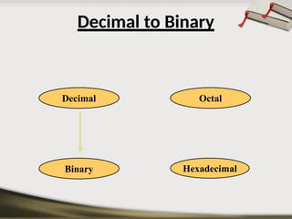
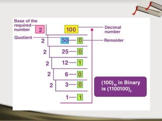
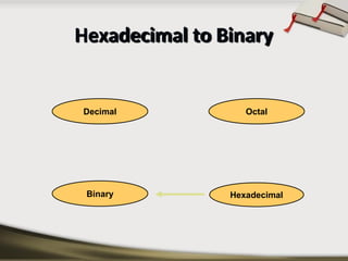
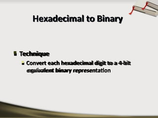
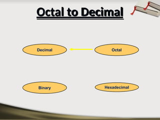
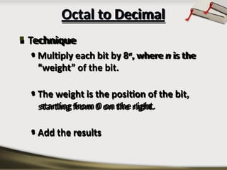
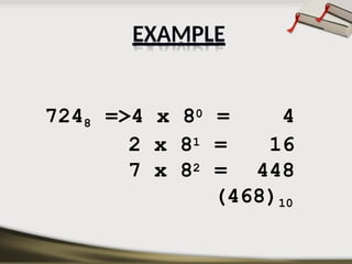
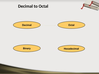
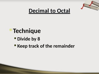
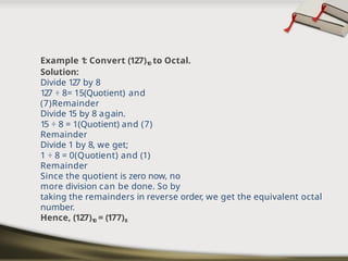
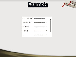
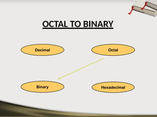
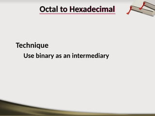
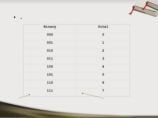
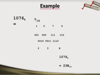
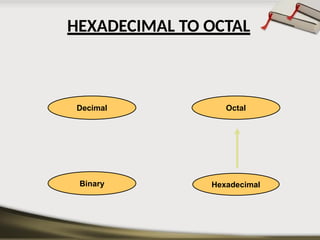
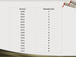
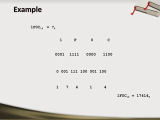
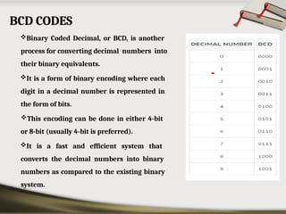
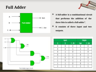
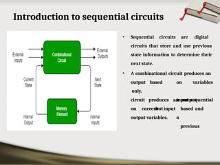
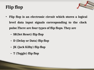
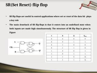
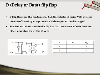
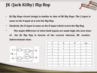
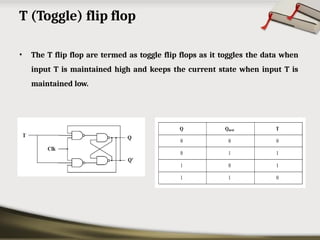
Basic Electrical and Electronics Engineering
Part – B
Unit 3 – Digital Electronics
By
Dr.S.A.Sivakumar [Dean-Academics, ASKW]
Mr.B.Naga Rajesh(Ph.D) [AP-ECE, ASKW]
Overview of Number Systems
A number system is defined as a system of writing to
express numbers.
It is the mathematical notation for representing
numbers of a given set by using digits or other symbols in a
consistent manner.
Types of Number Systems
The four most common number system types are:
Binary number system (Base- 2)
Decimal number system (Base- 10)
Octal number system (Base-8)
Hexadecimal number system (Base- 16)
Binary Number System (Base- 2)
The base 2 number system is also known as the Binary
Number System wherein, only two binary digits exist, i.e., 0
and 1.
The binary number system consists of two digits 0 and 1.
A binary digit is called a bit.
For example, 0101 is a binary number.
Decimal number system (Base- 10)
The decimal number system has the base (or) radix 10.
The decimal number system contain to 9 --0, 1, 2, 3, 4,
5, 6, 7, 8, 9.
Each symbol in the decimal number is called a digit. The
decimal number system is a positional weighted system;
each and every digit has a positional weight based on
position relative to the decimal point.
 For Example,the decimal number 1457 consists of the
digit 7 in the units position, 5 in the tens place, 4 in the
hundreds position, and 1 in the thousands place whose
value can be written as:
 (1×10³) + (4×10²) + (5×101) + (7×100)
 (1×1000) + (4×100) + (5×10) + (7×1)
 1000 + 400 + 50 + 7
 1457
Octal number system (Base- 8)
Its base or radix is ' 8 '.
It uses numbers from 0 to 7 to represent numbers. Octal
numbers are commonly used in computer applications.
Example: Convert 2158 into decimal. Solution:
2158 = 2 × 82 + 1 × 81 + 5 × 80
= 2 × 64 + 1 × 8 + 5 × 1
= 128 + 8 + 5
= 14110
Hexadecimal number system (Base- 16)
The Hexadecimal number system base/radix is 16.
In the hexadecimal system, the numbers
are
first
represented just like in the decimal system, i.e. from 0 to
9. Then, the numbers are represented using the alphabet
from A to F.
The below-given table shows the representation of
numbers in the hexadecimal number system.
Hexadec
imal
0 1 2 3 4 5 6 7 8 9 A B C D E F
Decimal 0 1 2 3 4 5 6 7 8 9 10 11 12 13 14 15
Conversion
of
Number
s
What we are going to explain
• Conversion between Binary & Decimal.
• Conversion between Decimal & Hexadecimal.
• Conversion between Hexadecimal & Binary.
• Conversion between Decimal & Octal.
• Conversion between Octal & Hexadecimal.
• Conversion between Binary & Octal.
The possibilities:
Hexadecimal
Decimal Octal
Binary
Conversion Among
Bases
Binary to Decimal
Hexadecimal
Decimal Octal
Binary
• Technique
–Multiply each bit by 2n, where n is
the “weight” of the bit.
–The weight is the position of the
bit, starting from 0 on the right.
–Add the results.
Binary to Decimal
(101011)2 1
2
0
=> 1 x 20 =
1 x 21
=
0 x 22
=
0
1 x 23
= 32
(43)10
Bit “0”
EXAMPLE
Decimal to Binary
Hexadecimal
Decimal Octal
Binary
Hexadecimal
Decimal Octal
Binary
Hexadecimal to Binary
Binary Hexadecimal
0000 0
0001 1
0010 2
0011 3
0100 4
0101 5
0110 6
0111 7
1000 8
1001 9
1010 A
1011 B
1100 C
1101 D
1110 E
1111 F
 Technique
 Convert each hexadecimal digit to a 4-bit
equivalent binary representation
Hexadecimal to Binary
Example
1 0 A F
0001 0000 1010 1111
10AF16 =
00010000101011112
10AF16 = ?2
Hexadecimal
Decimal Octal
Binary
Binary to Hexadecimal
⦿
Technique
› Group bits in fours, starting
on right
› Convert to hexadecimal digits
Example
10101110112 = ?16
10 1011 1011
2 B B
10101110112 = 2BB16
Hexadecimal
Decimal Octal
Binary
Octal to Decimal
Octal to Decimal
 Technique
• Multiply each bit by 8n, where n is the
“weight” of the bit.
• The weight is the position of the bit,
starting from 0 on the right.
• Add the results
7248 =>4 x 80 = 4
2 x 81 = 16
7 x 82 = 448
(468)10
EXAMPLE
Decimal to Octal
Hexadecimal
Decimal Octal
Binary
 Technique

Divide by 8

Keep track of the remainder
Decimal to Octal
Example 1: Convert (127)1
0 to Octal.
Solution:
Divide 127 by 8
127 ÷ 8= 15(Quotient) and
(7)Remainder
Divide 15 by 8 again.
15 ÷ 8 = 1(Quotient) and (7)
Remainder
Divide 1 by 8, we get;
1 ÷ 8 = 0(Quotient) and (1)
Remainder
Since the quotient is zero now, no
more division can be done. So by
taking the remainders in reverse order, we get the equivalent octal
number.
Hence, (127)1
0 = (177)8
Example
OCTAL TO BINARY
Hexadecimal
Decimal Octal
Binary
Octal to Binary
Hexadecimal
Decimal Octal
Binary
Binary to Octal
Binary to Octal
• Technique
– Group bits in threes, starting on right
– Convert to octal digits
10110101112 = ?8
1 011 010 111
1 3 2 7
10110101112 = 13278
Example
Hexadecimal
Decimal Octal
Binary
Hexadecimal to
Decimal
⚫Technique
⚫Multiply each bit by 16n, where n is the
“weight” of the bit
⚫The weight is the position of the bit, starting
from 0 on the right
⚫Add the results
Hexadecimal to Decimal
Example
ABC16 =>C x 160 = 12 x 1 = 12
B x 161 = 11 x 16 = 176
A x 162 = 10 x 256 = 2560
274810
Example
Hexadecimal
Decimal Octal
Binary
Decimal to Hexadecimal
▣ Technique
◾Divide by 16
◾Keep track of the remainder
Decimal to Hexadecimal
OCTAL TO HEXADECIMAL
Hexadecimal
Decimal Octal
Binary
Octal to Hexadecimal
Technique
Use binary as an intermediary
• .
Binary Octal
000 0
001 1
010 2
011 3
100 4
101 5
110 6
111 7
Example
10768
=
?16
1 0 7 6
001 000 111 110
0010 0011 1110
2 3 E
10768
= 23E16
Hexadecimal
Decimal Octal
Binary
HEXADECIMAL TO OCTAL
Hexadecimal to Octal
Technique
Use binary as an intermediary
Binary Hexadecimal
0000 0
0001 1
0010 2
0011 3
0100 4
0101 5
0110 6
0111 7
1000 8
1001 9
1010 A
1011 B
1100 C
1101 D
1110 E
1111 F
Example
1F0C16 = ?8
1 F 0 C
1 7 4 1 4
1F0C16 = 174148
0001 1111 0000 1100
0 001 111 100 001 100
BCD CODES
Binary Coded Decimal, or BCD, is another
process for converting decimal numbers into
their binary equivalents.
It is a form of binary encoding where each
digit in a decimal number is represented in
the form of bits.
This encoding can be done in either 4-bit
or 8-bit (usually 4-bit is preferred).
It is a fast and efficient system that
converts the decimal numbers into binary
numbers as compared to the existing binary
system.
For example:
Convert (123)10 in BCD
From the truth table above,
1 -> 0001
2 -> 0010
3 -> 0011
thus, BCD becomes -> 0001
0010 0011
Excess-3 code
 In this coding plan, each
decimal digit is tended to
by its relating 4-bit
double portrayal with the
extension of 3.
 Example – 1 : Decimal number of 9
Binary Representation of 9 is 1001
Now Add 3 to Each Bit: 1001 + 0011 = 1100
Therefore, 1100 is the Excess – 3 code for the decimal number 9
 Example – 2 : Decimal number of 15
Add 3 to 1 and 5 both separately after converting them into binary(4 bit). So,
1 = (0001)2 and 5 = (0101)2
Now add 3 to both the digit, 1+3 = 4 = (0100)2 and 5+3 = 8 = (1000)2
Therefore, 0100 1000 is the Excess – 3 code for the decimal number 15
Graycode
• A binary numbering system in
which two successive values only
differ by one bit is called gray
code
• Binary to Gray conversion :
1.The Most Significant Bit (MSB) of the gray code
is always equal to the MSB of the given binary
code.
2.Other bits of the output gray code can be
obtained by XORing binary code bit at
that index and previous index.
Example:
Binary 110111 - Gray 101100
• Gray to binary conversion :
• The Most Significant Bit (MSB) of the binary code is
always equal to the MSB of the given gray code.
• Other bits of the output binary code can be obtained
by checking the gray code bit at that index. If the
current gray code bit is 0, then copy the previous
binary code bit, else copy the invert of the previous
binary code bit.
Example:
Gray code : 11100 Binary : 10111
Hamming Code
• k parity bits are added to an n -bit data word to form
a new word of n + k bits
• Those positions numbered as a power of 2 are
reserved for the parity bits
• The remaining bits are the data bits
Logic gates including Universal Gates
 There are seven basic logic gates: AND, OR, XOR, NOT, NAND,
NOR and XNOR.
AND gate
The AND gate is named so because, if 0 is false and 1 is
true, the gate acts in the same way as the logical "and"
operator.
The output is "true" when both inputs are "true." Otherwise,
the output is "false." In other words, the output is 1 only when
both inputs are 1.
OR gate
The OR gate gets its name from behaving like the
logical inclusive "or."
The output is true if one or both of the inputs are true.
If both inputs are false, then the output is false.
In other words, for the output to be 1, at least one
input must be 1.
XOR gate
The XOR (exclusive-OR) gate acts in the same way as
the logical "either/or."
The output is true if either, but not both, of the inputs
are true.
The output is false if both inputs are "false" or if both
inputs are true.
Similarly, the output is 1 if the inputs are different but
0 if the inputs are the same.
• A NOT gate reverses the logic state. If the input
is 1, then the output is 0. If the input is 0, then
the output is 1.
NOT gate
NAND gate
The NAND (Negated AND) gate operates as an AND
gate followed by a NOT gate.
It acts in the manner of the logical operation "and"
followed by negation.
The output is false if both inputs are true.
NOR gate
The NOR (NOT OR) gate is a combination OR
gate followed by an inverter.
Its output is true if both inputs are false. Otherwise,
the output is false.
XNOR gate
The XNOR (exclusive-NOR) gate is a combination of an
XOR gate followed by an inverter.
Its output is true if the inputs are the same and false if
the inputs are different.
XNOR gate
The XNOR (exclusive-NOR) gate is a combination of an
XOR gate followed by an inverter.
Its output is true if the inputs are the same and false if
the inputs are different.
Universal Gates
• NAND
• NOR
NAND gate and NOR gate can be termed as
universal logic gates since any Boolean function
can be implemented using NAND gate or NOR
gate
Boolean Algebra
• Boolean algebra is a branch of mathematics that deals
with operations on logical values with binary
variables.
• Boolean variables are represented as binary numbers
to represent truths: 1 = true and 0 = false.
• Elementary algebra deals with numerical operations,
whereas Boolean algebra deals with logical operations.
De Morgan's Theorem 1
Theorem 1 A + B = A .
B
The complement of the union of two sets is equal
to the intersection of the complements of each set.
De Morgan's Theorem 2
Theorem 2 A . B = A +
B
The complement of intersection of two sets is
equal to the union of the complements of each set.
Properties of Boolean Algebra
• T1 : Properties of 0
–(a) 0 + A = A
(b) 0 A = 0
• T2 : Properties of 1
–(a) 1 + A = 1
(b) 1 A = A
Properties of Boolean Algebra
• T3 : Commutative Law
– (a) A + B = B + A
(b) A B = B A
• T4 : Associate Law
– (a) (A + B) + C = A + (B + C)
(b) (A B) C = A (B C)
• T5 : Distributive Law
– (a) A (B + C) = A B + A C
(b) A + (B C) = (A + B) (A + C)
Properties of Boolean Algebra
• T6 : Indempotence (Identity ) Law
– (a) A + A = A
(b) A A = A
• T7 : Absorption (Redundance) Law
– (a) A + A B = A
(b) A (A + B) = A
Properties of Boolean Algebra
• T8 : Complementary Law
– (a) X+X’=1
– (b) X.X’=0
• T9 : Involution
– (a) x’’ = x
Combinational Circuits
• A combinational logic circuit is a digital circuit that
produces an output based on the current inputs,
without any internal memory or feedback.
• The output is a function of the current inputs, and is
not dependent on the history of input signals.
Half Adder
A Combinational circuit that performs the
arithmetic addition of two bits is called as half
adder.
The output of Ex-OR gate is called Sum, while
output of AND gate is carry.
The input variables of a half-adder are called the
augends & addend bits.
The output variables are Sum & Carry.
Full Adder
 A full-adder is a combinational circuit
that performs the addition of the
three bits is called a full-adder".
 It consists of three input and two
outputs.
Introduction to sequential circuits
• Sequential circuits are digital
circuits that store and use previous
state information to determine their
next state.
• A combinational circuit produces an
based on
input
but
a
variables
sequential
output
only,
circuit produces an output
based and
previous
on current input
output variables.
Flip flop
• Flip flop is an electronic circuit which stores a logical
level data input signals corresponding to the clock
pulse.There are four types of flip flops. They are
– SR(Set Reset) flip flop
– D (Delay or Data) flip flop
– JK (Jack Kilby) flip flop
– T (Toggle) flip flop
SR(Set Reset) flip flop
• SR flip flops are useful in control applications where set or reset of the data bit plays
a key role
• The main drawback of SR flip-flops is that it enters into an undefined state when
both inputs are made high simultaneously. The structure of SR flip flop is given in
Figure
D (Delay or Data) flip flop
• D-Flip flops are the fundamental building blocks of major VLSI systems
because of its ability to capture data with respect to the clock signal.
• The data will be retained in the flip flop until the arrival of next clock and
other input changes will be ignored
JK (Jack Kilby) flip flop
• JK flip flops circuit design is similar to that of SR flip flops. The J input is
same as the S input as it sets the flip-flop.
• Similarly, the K input is same as the R input which resets the flip flop.
• The major difference is when both inputs are made high, the next state
of the JK flip flop is inverse of the current whereas SR reaches
indeterminate state.
T (Toggle) flip flop
• The T flip flop are termed as toggle flip flops as it toggles the data when
input T is maintained high and keeps the current state when input T is
maintained low.
Registers
 Flip flops can be used to store a single bit of binary data (1 or 0)
 N flip flops are to be connected in order to store n bits of data.
 Shift Register is a group of flip flops used to store multiple bits of
data.
 The bits stored in such registers can be made to move within the
registers and in/out of the registers by applying clock pulses.
 An n-bit shift register can be formed by connecting n flip-flops where
each flip-flop stores a single bit of data.
 The registers which will shift the bits to the left are called “Shift left
registers”.
 The registers which will shift the bits to the right are called “Shift
right registers”.
• Shift registers are basically of following types.
– Serial In Serial Out shift register
– Serial In parallel Out shift register
– Parallel In Serial Out shift register
– Parallel In parallel Out shift register
Serial In Serial Out shift register
 Data at the input will be delayed by four clock periods from the input to
the output of the shift register.
– Data at “data in” will be present at the Stage A output after the first clock pulse.
– After the second pulse, stage A data is transferred to stage B output, and “data in” is
transferred to stage A output.
– After the third clock, stage C is replaced by stage B; stage B is replaced by stage A; and
stage A is replaced by “data in”.
– After the fourth clock, the data originally present at “data in” is at stage D, “output”.
– The “first in” data is “first out” as it is shifted from “data in” to “data out”.
Serial In parallel Out shift register
 In Figure below, four data bits will be shifted in from “data in” by four
clock pulses and be available at QA through QD
– After the first clock, the data at “data in” appears at QA.
– After the second clock, the old QA data appears at QB; QA receives the next data from “data
in”.
– After the third clock, QB data is at QC.
– After the fourth clock, QC data is at QD. This stage contains the data first present at “data
in”. The shift register now contains four data bits.
Parallel In Serial Out shift register
 Data is loaded into all stages at once in a parallel-in/serial-out shift
register. The data is then shifted out via “data out” by clock pulses.
Since a 4- stage shift register is shown below, four clock pulses are
required to shift out all of the data.
 In Figure below, stage D data will be present at the “data out” up until the first
clock pulse.
 Stage C data will be present at “data out” between the first clock and the second
clock pulse.
 Stage B data will be present between the second clock and the third clock
 Stage A data will be present between the third and the fourth clock.
Parallel In parallel Out shift register
• As shown in Figure below, a parallel-in/parallel-out shift register combines
the function of the parallel-in, serial-out shift register with the function of
the serial-in, parallel-out shift register to yield the universal shift register.
• Data presented at DA through DD is parallel loaded into the registers. This
data at QA through QD may be shifted by the number of pulses presented at
the clock input. The shifted data is available at QA through QD.
Counters
• A special type of sequential circuit used to count the pulse is known as a
counter, or a collection of flip flops where the clock signal is applied is known as
counters.
• The counter is one of the widest applications of the flip flop. Based on the clock
pulse, the output of the counter contains a predefined state. The number of the
pulse can be counted using the output of the counter.
Truth Table Types of Counters
•Asynchronous Counters
•Synchronous Counters
Asynchronous Counters
• The Asynchronous counter is also known as the ripple counter. Below is a
diagram of the 2-bit Asynchronous counter in which we used two T flip-flops.
Apart from the T flip flop, we can also use the JK flip flop by setting both of
the inputs to 1 permanently.
• The external clock pass to the clock input of the first flip flop, i.e., FF-A and its
output, i.e., is passed to clock input of the next flip flop, i.e., FF-B
Condition 1
: When both the flip flops are in reset condition.
Operation: The outputs of both flip flops, i.e., QA QB, will be 0.
Condition 2: When the first negative clock edge passes.
Operation: The first flip flop will toggle, and the output of this flip flop will
change from 0 to 1
. The output of this flip flop will be taken by the clock
input of the next flip flop. This output will be taken as a positive edge
clock by the second flip flop. This input will not change the second flip
flop's output state because it is the negative edge
triggered flip flop. So, QA = 1 and QB = 0
Condition 3: When the second negative clock edge is applied.
Operation: The first flip flop will toggle again, and the output of this flip
flop will change from 1 to 0. This output will be taken as a negative edge
clock by the second flip flop. This input will change the second flip flop's
output state because it is the negative edge triggered
flip flop. So, QA = 0 and QB = 1
.
Condition 4: When the third negative clock edge is applied.
Operation: The first flip flop will toggle again, and the output of this flip
flop will change from 0 to 1
. This output will be taken as a positive edge
clock by the second flip flop. This input will not change the second flip
flop's output state because it is the negative edge triggered
flip flop. So, QA = 1 and QB = 1
Condition 5: When the fourth negative clock edge is applied.
Operation: The first flip flop will toggle again, and the output of this flip
flop will change from 1 to 0. This output will be taken as a negative edge
clock by the second flip flop. This input will change the output state of
the second
flip
flop.
So,
QA = 0 and QB =
0
3-bit counter ( can work as both up & down
Counter)
Down Counter
Synchronous counters
In the Asynchronous counter, the present counter's output passes to
the input of the next counter. So, the counters are connected like a
chain. The drawback of this system is that it creates the counting delay,
and the propagation delay also occurs during the counting stage.
The synchronous counter is designed to remove this drawback.
In the synchronous counter, the same clock pulse is passed to the
clock input of all the flip flops. The clock signals produced by all the
flip flops are the same as each other. Below is the diagram of a 2-bit
synchronous counter in which the inputs of the first flip flop, i.e., FF-A,
are set to 1
. So, the first flip flop will work as a toggle flip-flop. The
output of the first flip flop is passed to both the inputs of the next JK
flip flop.
BEEE - Part B - Unit 3 - Digital Electronics PPT.pptx

BEEE - Part B - Unit 3 - Digital Electronics PPT.pptx

  • 1.
    Basic Electrical andElectronics Engineering Part – B Unit 3 – Digital Electronics By Dr.S.A.Sivakumar [Dean-Academics, ASKW] Mr.B.Naga Rajesh(Ph.D) [AP-ECE, ASKW]
  • 2.
    Overview of NumberSystems A number system is defined as a system of writing to express numbers. It is the mathematical notation for representing numbers of a given set by using digits or other symbols in a consistent manner.
  • 3.
    Types of NumberSystems The four most common number system types are: Binary number system (Base- 2) Decimal number system (Base- 10) Octal number system (Base-8) Hexadecimal number system (Base- 16)
  • 4.
    Binary Number System(Base- 2) The base 2 number system is also known as the Binary Number System wherein, only two binary digits exist, i.e., 0 and 1. The binary number system consists of two digits 0 and 1. A binary digit is called a bit. For example, 0101 is a binary number.
  • 5.
    Decimal number system(Base- 10) The decimal number system has the base (or) radix 10. The decimal number system contain to 9 --0, 1, 2, 3, 4, 5, 6, 7, 8, 9. Each symbol in the decimal number is called a digit. The decimal number system is a positional weighted system; each and every digit has a positional weight based on position relative to the decimal point.
  • 6.
     For Example,thedecimal number 1457 consists of the digit 7 in the units position, 5 in the tens place, 4 in the hundreds position, and 1 in the thousands place whose value can be written as:  (1×10³) + (4×10²) + (5×101) + (7×100)  (1×1000) + (4×100) + (5×10) + (7×1)  1000 + 400 + 50 + 7  1457
  • 7.
    Octal number system(Base- 8) Its base or radix is ' 8 '. It uses numbers from 0 to 7 to represent numbers. Octal numbers are commonly used in computer applications. Example: Convert 2158 into decimal. Solution: 2158 = 2 × 82 + 1 × 81 + 5 × 80 = 2 × 64 + 1 × 8 + 5 × 1 = 128 + 8 + 5 = 14110
  • 8.
    Hexadecimal number system(Base- 16) The Hexadecimal number system base/radix is 16. In the hexadecimal system, the numbers are first represented just like in the decimal system, i.e. from 0 to 9. Then, the numbers are represented using the alphabet from A to F. The below-given table shows the representation of numbers in the hexadecimal number system. Hexadec imal 0 1 2 3 4 5 6 7 8 9 A B C D E F Decimal 0 1 2 3 4 5 6 7 8 9 10 11 12 13 14 15
  • 9.
  • 10.
    What we aregoing to explain • Conversion between Binary & Decimal. • Conversion between Decimal & Hexadecimal. • Conversion between Hexadecimal & Binary. • Conversion between Decimal & Octal. • Conversion between Octal & Hexadecimal. • Conversion between Binary & Octal.
  • 11.
  • 12.
  • 13.
    • Technique –Multiply eachbit by 2n, where n is the “weight” of the bit. –The weight is the position of the bit, starting from 0 on the right. –Add the results. Binary to Decimal
  • 14.
    (101011)2 1 2 0 => 1x 20 = 1 x 21 = 0 x 22 = 0 1 x 23 = 32 (43)10 Bit “0” EXAMPLE
  • 15.
  • 17.
  • 18.
    Binary Hexadecimal 0000 0 00011 0010 2 0011 3 0100 4 0101 5 0110 6 0111 7 1000 8 1001 9 1010 A 1011 B 1100 C 1101 D 1110 E 1111 F
  • 19.
     Technique  Converteach hexadecimal digit to a 4-bit equivalent binary representation Hexadecimal to Binary
  • 20.
    Example 1 0 AF 0001 0000 1010 1111 10AF16 = 00010000101011112 10AF16 = ?2
  • 21.
  • 22.
    Binary to Hexadecimal ⦿ Technique ›Group bits in fours, starting on right › Convert to hexadecimal digits
  • 23.
    Example 10101110112 = ?16 101011 1011 2 B B 10101110112 = 2BB16
  • 24.
  • 25.
    Octal to Decimal Technique • Multiply each bit by 8n, where n is the “weight” of the bit. • The weight is the position of the bit, starting from 0 on the right. • Add the results
  • 26.
    7248 =>4 x80 = 4 2 x 81 = 16 7 x 82 = 448 (468)10 EXAMPLE
  • 27.
  • 28.
     Technique  Divide by8  Keep track of the remainder Decimal to Octal
  • 29.
    Example 1: Convert(127)1 0 to Octal. Solution: Divide 127 by 8 127 ÷ 8= 15(Quotient) and (7)Remainder Divide 15 by 8 again. 15 ÷ 8 = 1(Quotient) and (7) Remainder Divide 1 by 8, we get; 1 ÷ 8 = 0(Quotient) and (1) Remainder Since the quotient is zero now, no more division can be done. So by taking the remainders in reverse order, we get the equivalent octal number. Hence, (127)1 0 = (177)8
  • 30.
  • 31.
  • 32.
  • 33.
  • 34.
    Binary to Octal •Technique – Group bits in threes, starting on right – Convert to octal digits
  • 35.
    10110101112 = ?8 1011 010 111 1 3 2 7 10110101112 = 13278 Example
  • 36.
  • 37.
    ⚫Technique ⚫Multiply each bitby 16n, where n is the “weight” of the bit ⚫The weight is the position of the bit, starting from 0 on the right ⚫Add the results Hexadecimal to Decimal
  • 38.
  • 39.
    ABC16 =>C x160 = 12 x 1 = 12 B x 161 = 11 x 16 = 176 A x 162 = 10 x 256 = 2560 274810 Example
  • 40.
  • 41.
    Decimal to Hexadecimal ▣Technique ◾Divide by 16 ◾Keep track of the remainder
  • 42.
  • 43.
  • 44.
    Octal to Hexadecimal Technique Usebinary as an intermediary
  • 45.
    • . Binary Octal 0000 001 1 010 2 011 3 100 4 101 5 110 6 111 7
  • 46.
    Example 10768 = ?16 1 0 76 001 000 111 110 0010 0011 1110 2 3 E 10768 = 23E16
  • 47.
  • 48.
    Hexadecimal to Octal Technique Usebinary as an intermediary
  • 49.
    Binary Hexadecimal 0000 0 00011 0010 2 0011 3 0100 4 0101 5 0110 6 0111 7 1000 8 1001 9 1010 A 1011 B 1100 C 1101 D 1110 E 1111 F
  • 50.
    Example 1F0C16 = ?8 1F 0 C 1 7 4 1 4 1F0C16 = 174148 0001 1111 0000 1100 0 001 111 100 001 100
  • 51.
    BCD CODES Binary CodedDecimal, or BCD, is another process for converting decimal numbers into their binary equivalents. It is a form of binary encoding where each digit in a decimal number is represented in the form of bits. This encoding can be done in either 4-bit or 8-bit (usually 4-bit is preferred). It is a fast and efficient system that converts the decimal numbers into binary numbers as compared to the existing binary system.
  • 52.
    For example: Convert (123)10in BCD From the truth table above, 1 -> 0001 2 -> 0010 3 -> 0011 thus, BCD becomes -> 0001 0010 0011
  • 53.
    Excess-3 code  Inthis coding plan, each decimal digit is tended to by its relating 4-bit double portrayal with the extension of 3.
  • 54.
     Example –1 : Decimal number of 9 Binary Representation of 9 is 1001 Now Add 3 to Each Bit: 1001 + 0011 = 1100 Therefore, 1100 is the Excess – 3 code for the decimal number 9  Example – 2 : Decimal number of 15 Add 3 to 1 and 5 both separately after converting them into binary(4 bit). So, 1 = (0001)2 and 5 = (0101)2 Now add 3 to both the digit, 1+3 = 4 = (0100)2 and 5+3 = 8 = (1000)2 Therefore, 0100 1000 is the Excess – 3 code for the decimal number 15
  • 55.
    Graycode • A binarynumbering system in which two successive values only differ by one bit is called gray code
  • 56.
    • Binary toGray conversion : 1.The Most Significant Bit (MSB) of the gray code is always equal to the MSB of the given binary code. 2.Other bits of the output gray code can be obtained by XORing binary code bit at that index and previous index. Example: Binary 110111 - Gray 101100
  • 57.
    • Gray tobinary conversion : • The Most Significant Bit (MSB) of the binary code is always equal to the MSB of the given gray code. • Other bits of the output binary code can be obtained by checking the gray code bit at that index. If the current gray code bit is 0, then copy the previous binary code bit, else copy the invert of the previous binary code bit. Example: Gray code : 11100 Binary : 10111
  • 58.
    Hamming Code • kparity bits are added to an n -bit data word to form a new word of n + k bits • Those positions numbered as a power of 2 are reserved for the parity bits • The remaining bits are the data bits
  • 61.
    Logic gates includingUniversal Gates  There are seven basic logic gates: AND, OR, XOR, NOT, NAND, NOR and XNOR. AND gate The AND gate is named so because, if 0 is false and 1 is true, the gate acts in the same way as the logical "and" operator. The output is "true" when both inputs are "true." Otherwise, the output is "false." In other words, the output is 1 only when both inputs are 1.
  • 63.
    OR gate The ORgate gets its name from behaving like the logical inclusive "or." The output is true if one or both of the inputs are true. If both inputs are false, then the output is false. In other words, for the output to be 1, at least one input must be 1.
  • 64.
    XOR gate The XOR(exclusive-OR) gate acts in the same way as the logical "either/or." The output is true if either, but not both, of the inputs are true. The output is false if both inputs are "false" or if both inputs are true. Similarly, the output is 1 if the inputs are different but 0 if the inputs are the same.
  • 66.
    • A NOTgate reverses the logic state. If the input is 1, then the output is 0. If the input is 0, then the output is 1. NOT gate
  • 67.
    NAND gate The NAND(Negated AND) gate operates as an AND gate followed by a NOT gate. It acts in the manner of the logical operation "and" followed by negation. The output is false if both inputs are true.
  • 68.
    NOR gate The NOR(NOT OR) gate is a combination OR gate followed by an inverter. Its output is true if both inputs are false. Otherwise, the output is false.
  • 69.
    XNOR gate The XNOR(exclusive-NOR) gate is a combination of an XOR gate followed by an inverter. Its output is true if the inputs are the same and false if the inputs are different.
  • 70.
    XNOR gate The XNOR(exclusive-NOR) gate is a combination of an XOR gate followed by an inverter. Its output is true if the inputs are the same and false if the inputs are different.
  • 71.
    Universal Gates • NAND •NOR NAND gate and NOR gate can be termed as universal logic gates since any Boolean function can be implemented using NAND gate or NOR gate
  • 72.
    Boolean Algebra • Booleanalgebra is a branch of mathematics that deals with operations on logical values with binary variables. • Boolean variables are represented as binary numbers to represent truths: 1 = true and 0 = false. • Elementary algebra deals with numerical operations, whereas Boolean algebra deals with logical operations.
  • 73.
    De Morgan's Theorem1 Theorem 1 A + B = A . B The complement of the union of two sets is equal to the intersection of the complements of each set.
  • 74.
    De Morgan's Theorem2 Theorem 2 A . B = A + B The complement of intersection of two sets is equal to the union of the complements of each set.
  • 75.
    Properties of BooleanAlgebra • T1 : Properties of 0 –(a) 0 + A = A (b) 0 A = 0 • T2 : Properties of 1 –(a) 1 + A = 1 (b) 1 A = A
  • 76.
    Properties of BooleanAlgebra • T3 : Commutative Law – (a) A + B = B + A (b) A B = B A • T4 : Associate Law – (a) (A + B) + C = A + (B + C) (b) (A B) C = A (B C) • T5 : Distributive Law – (a) A (B + C) = A B + A C (b) A + (B C) = (A + B) (A + C)
  • 77.
    Properties of BooleanAlgebra • T6 : Indempotence (Identity ) Law – (a) A + A = A (b) A A = A • T7 : Absorption (Redundance) Law – (a) A + A B = A (b) A (A + B) = A
  • 78.
    Properties of BooleanAlgebra • T8 : Complementary Law – (a) X+X’=1 – (b) X.X’=0 • T9 : Involution – (a) x’’ = x
  • 79.
    Combinational Circuits • Acombinational logic circuit is a digital circuit that produces an output based on the current inputs, without any internal memory or feedback. • The output is a function of the current inputs, and is not dependent on the history of input signals.
  • 80.
    Half Adder A Combinationalcircuit that performs the arithmetic addition of two bits is called as half adder. The output of Ex-OR gate is called Sum, while output of AND gate is carry. The input variables of a half-adder are called the augends & addend bits. The output variables are Sum & Carry.
  • 81.
    Full Adder  Afull-adder is a combinational circuit that performs the addition of the three bits is called a full-adder".  It consists of three input and two outputs.
  • 82.
    Introduction to sequentialcircuits • Sequential circuits are digital circuits that store and use previous state information to determine their next state. • A combinational circuit produces an based on input but a variables sequential output only, circuit produces an output based and previous on current input output variables.
  • 83.
    Flip flop • Flipflop is an electronic circuit which stores a logical level data input signals corresponding to the clock pulse.There are four types of flip flops. They are – SR(Set Reset) flip flop – D (Delay or Data) flip flop – JK (Jack Kilby) flip flop – T (Toggle) flip flop
  • 84.
    SR(Set Reset) flipflop • SR flip flops are useful in control applications where set or reset of the data bit plays a key role • The main drawback of SR flip-flops is that it enters into an undefined state when both inputs are made high simultaneously. The structure of SR flip flop is given in Figure
  • 85.
    D (Delay orData) flip flop • D-Flip flops are the fundamental building blocks of major VLSI systems because of its ability to capture data with respect to the clock signal. • The data will be retained in the flip flop until the arrival of next clock and other input changes will be ignored
  • 86.
    JK (Jack Kilby)flip flop • JK flip flops circuit design is similar to that of SR flip flops. The J input is same as the S input as it sets the flip-flop. • Similarly, the K input is same as the R input which resets the flip flop. • The major difference is when both inputs are made high, the next state of the JK flip flop is inverse of the current whereas SR reaches indeterminate state.
  • 87.
    T (Toggle) flipflop • The T flip flop are termed as toggle flip flops as it toggles the data when input T is maintained high and keeps the current state when input T is maintained low.
  • 88.
    Registers  Flip flopscan be used to store a single bit of binary data (1 or 0)  N flip flops are to be connected in order to store n bits of data.  Shift Register is a group of flip flops used to store multiple bits of data.  The bits stored in such registers can be made to move within the registers and in/out of the registers by applying clock pulses.  An n-bit shift register can be formed by connecting n flip-flops where each flip-flop stores a single bit of data.  The registers which will shift the bits to the left are called “Shift left registers”.  The registers which will shift the bits to the right are called “Shift right registers”.
  • 89.
    • Shift registersare basically of following types. – Serial In Serial Out shift register – Serial In parallel Out shift register – Parallel In Serial Out shift register – Parallel In parallel Out shift register
  • 90.
    Serial In SerialOut shift register  Data at the input will be delayed by four clock periods from the input to the output of the shift register. – Data at “data in” will be present at the Stage A output after the first clock pulse. – After the second pulse, stage A data is transferred to stage B output, and “data in” is transferred to stage A output. – After the third clock, stage C is replaced by stage B; stage B is replaced by stage A; and stage A is replaced by “data in”. – After the fourth clock, the data originally present at “data in” is at stage D, “output”. – The “first in” data is “first out” as it is shifted from “data in” to “data out”.
  • 91.
    Serial In parallelOut shift register  In Figure below, four data bits will be shifted in from “data in” by four clock pulses and be available at QA through QD – After the first clock, the data at “data in” appears at QA. – After the second clock, the old QA data appears at QB; QA receives the next data from “data in”. – After the third clock, QB data is at QC. – After the fourth clock, QC data is at QD. This stage contains the data first present at “data in”. The shift register now contains four data bits.
  • 92.
    Parallel In SerialOut shift register  Data is loaded into all stages at once in a parallel-in/serial-out shift register. The data is then shifted out via “data out” by clock pulses. Since a 4- stage shift register is shown below, four clock pulses are required to shift out all of the data.  In Figure below, stage D data will be present at the “data out” up until the first clock pulse.  Stage C data will be present at “data out” between the first clock and the second clock pulse.  Stage B data will be present between the second clock and the third clock  Stage A data will be present between the third and the fourth clock.
  • 93.
    Parallel In parallelOut shift register • As shown in Figure below, a parallel-in/parallel-out shift register combines the function of the parallel-in, serial-out shift register with the function of the serial-in, parallel-out shift register to yield the universal shift register. • Data presented at DA through DD is parallel loaded into the registers. This data at QA through QD may be shifted by the number of pulses presented at the clock input. The shifted data is available at QA through QD.
  • 94.
    Counters • A specialtype of sequential circuit used to count the pulse is known as a counter, or a collection of flip flops where the clock signal is applied is known as counters. • The counter is one of the widest applications of the flip flop. Based on the clock pulse, the output of the counter contains a predefined state. The number of the pulse can be counted using the output of the counter. Truth Table Types of Counters •Asynchronous Counters •Synchronous Counters
  • 95.
    Asynchronous Counters • TheAsynchronous counter is also known as the ripple counter. Below is a diagram of the 2-bit Asynchronous counter in which we used two T flip-flops. Apart from the T flip flop, we can also use the JK flip flop by setting both of the inputs to 1 permanently. • The external clock pass to the clock input of the first flip flop, i.e., FF-A and its output, i.e., is passed to clock input of the next flip flop, i.e., FF-B
  • 96.
    Condition 1 : Whenboth the flip flops are in reset condition. Operation: The outputs of both flip flops, i.e., QA QB, will be 0. Condition 2: When the first negative clock edge passes. Operation: The first flip flop will toggle, and the output of this flip flop will change from 0 to 1 . The output of this flip flop will be taken by the clock input of the next flip flop. This output will be taken as a positive edge clock by the second flip flop. This input will not change the second flip flop's output state because it is the negative edge triggered flip flop. So, QA = 1 and QB = 0 Condition 3: When the second negative clock edge is applied. Operation: The first flip flop will toggle again, and the output of this flip flop will change from 1 to 0. This output will be taken as a negative edge clock by the second flip flop. This input will change the second flip flop's output state because it is the negative edge triggered flip flop. So, QA = 0 and QB = 1 .
  • 97.
    Condition 4: Whenthe third negative clock edge is applied. Operation: The first flip flop will toggle again, and the output of this flip flop will change from 0 to 1 . This output will be taken as a positive edge clock by the second flip flop. This input will not change the second flip flop's output state because it is the negative edge triggered flip flop. So, QA = 1 and QB = 1 Condition 5: When the fourth negative clock edge is applied. Operation: The first flip flop will toggle again, and the output of this flip flop will change from 1 to 0. This output will be taken as a negative edge clock by the second flip flop. This input will change the output state of the second flip flop. So, QA = 0 and QB = 0
  • 98.
    3-bit counter (can work as both up & down Counter)
  • 99.
  • 100.
    Synchronous counters In theAsynchronous counter, the present counter's output passes to the input of the next counter. So, the counters are connected like a chain. The drawback of this system is that it creates the counting delay, and the propagation delay also occurs during the counting stage. The synchronous counter is designed to remove this drawback. In the synchronous counter, the same clock pulse is passed to the clock input of all the flip flops. The clock signals produced by all the flip flops are the same as each other. Below is the diagram of a 2-bit synchronous counter in which the inputs of the first flip flop, i.e., FF-A, are set to 1 . So, the first flip flop will work as a toggle flip-flop. The output of the first flip flop is passed to both the inputs of the next JK flip flop.