Download to read offline


![International Research Journal of Engineering and Technology (IRJET) e-ISSN: 2395-0056
Volume: 04 Issue: 10 | Oct -2017 www.irjet.net p-ISSN: 2395-0072
© 2017, IRJET | Impact Factor value: 5.181 | ISO 9001:2008 Certified Journal | Page 391
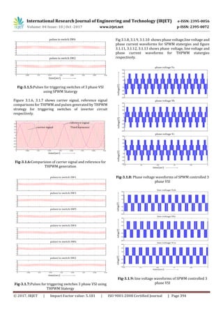
THD analysis of SPWM & THPWM Controlled Three phase Voltage
Source Inverter
Mohd Esa1 and Mohd Abdul Muqeem Nawaz2
1,2M.E. Student, EED, Muffakham Jah College of Engineering and Technology, Hyderabad, India
---------------------------------------------------------------------***---------------------------------------------------------------------
Abstract –The aim of this paper is to determine the Total
harmonic distortion (THD) of three phase voltage source
inverter (VSI) fed R-L load. The modulation Techniques usedis
Sinusoidal pulse width modulation (SPWM) and third
harmonic pulse width modulation (THPWM). The Carrier
frequency is varied to analyze its effect on Current THD and
Voltage THD.This paper also presents the comparison of
SPWM and THPWM controlled Inverter in terms of THD. The
simulation result shows THPWMhasbetter performancewhen
compared to SPWM. The simulation of circuit is done by using
MATLAB/Simulink.
Key Words: SPWM, THPWM, THD, Carrier Frequency.
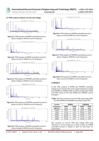
1. INTRODUCTION
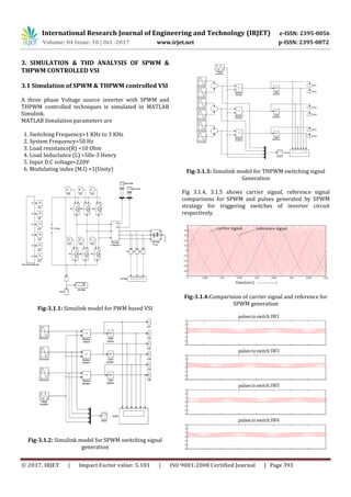
1.1 Stepped & PWM Inverters
Inverter converts input DC voltage into a.c. output voltage.
Three phase inverters are normally used for high power
applications [1].The applications of inverters include
uninterrupted power supply (UPS), a.c. motor speed
controllers etc. Voltage source inverter is capable of
supplying variable frequency variable voltage for speed
control of induction motors.VSI can be operated as stepped
wave inverter or a pulse width modulated (PWM) inverter.
For stepped wave inverter Output voltage can be varied by
varying input DC voltage. When input voltage is DC, variable
DC input voltage is obtained by connecting a chopper
between DC supply and inverter. When input voltage is a.c.,
variable DC input is obtained by connecting a controlled
rectifier between a.c. supply and inverter. The disadvantage
of stepped wave inverterislargeharmonicsoflowfrequency
in output voltage. Due to this low frequency harmonics, the
motor losses are increased at all speeds causing derating of
Motor. Harmonics content in induction motor current
increases at low speeds. The above drawbacks are
eliminated by using Pulse Width Modulated(PWM)inverter.
Harmonics and losses get reduced in PWM inverters.
For PWM inverter output voltage and frequency can be
controlled without external control. When input voltage is
DC, it is directly connected to PWM inverter. When the input
voltage is a.c., DC is obtained by connecting a diode bridge
rectifier and output of rectifier is connected to PWM
inverter.PWM basedinverterisconsideredinthis paper over
stepped wave inverter because of its harmonics reduction
ability.
1.2 Control Strategies
Various PWM control strategies have been developed in the
past two decades [2].To obtain variation of output voltage
and frequency PWM control strategies such as Sinusoidal
pulse width modulation (SPWM),Third harmonic pulse
width modulation (THPWM), Space vector pulse width
modulation(SVPWM) and 60° PWM are most commonly
used for three phase inverters. SPWM is simplest of all the
above PWM techniques. It was introduced by schonung and
stemmler in 1964[3]. The required signals for gates of
inverter are generated by comparing reference sine wave
and triangular carrier signal in SPWM technique. In 1975
Buja developed THPWM technique.THPWM is implemented
in same manner as SPWM the difference is thatreference a.c.
waveform is not sinusoidal but consists of bothfundamental
component and third harmonic component[1],[4]. The
advantages of PWM techniques are that they are easy to
implement and control, reduces lower order harmonics
[5].SPWM and THPWM techniques are analyzed and
compared in terms of harmonics in this paper.
1.3 Total harmonic distortion
Harmonic distortion is caused bynonlineardevicesinpower
system. A nonlinear device is one in which current is not
proportional to applied voltage.IEEE Standard 519-1992
recommends the requirements for harmonic control in
electrical power systems [6]. Thequalityof Outputvoltage of
inverter strongly related to total harmonic distortion
[7].THD is the measure of effective value of harmonic
components of a distorted waveform.
Where h is characteristic harmonic order, is harmonic
voltage and is fundamental voltage.](https://image.slidesharecdn.com/ilovepdfmerged40-200326112403/85/Multilevel-Inverter-and-Multipliers-11-320.jpg)
![International Research Journal of Engineering and Technology (IRJET) e-ISSN: 2395-0056
Volume: 04 Issue: 10 | Oct -2017 www.irjet.net p-ISSN: 2395-0072
© 2017, IRJET | Impact Factor value: 5.181 | ISO 9001:2008 Certified Journal | Page 398
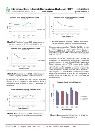
Chart-4.6: Comparison of current THD’s for SPWM and
THPWM controlled VSI
5. CONCLUSIONS
A three phase VSI has been implemented with SPWM and
THPWM control strategies. Analysis of current THD and
voltage THD is done at carrier frequencies from 1000Hz to
3000Hz.Simulation results of SPWM controlled inverterand
THPWM controlled inverter are compared. From chart 4.5
and chart 4.6 it can be concluded that THPWM provides
better quality of output voltage and current whencompared
to SPWM controlled inverter i.e. both current THD and
voltage THD is lesser in case of THPWM.Although there is
variation in current THD and Voltage THD with variation in
Carrier frequency, it is clear that current THD is well below
5% as specified by IEEE standards in both SPWM & THPWM
inverters.
REFERENCES
[1] Muhammad H. Rashid, “Power Electronics-Circuits,
Devices and Applications” Pearson Education Incorporated,
2005.
[2] R.K. Pongiannan, and N. Yadaiah, “FPGA Based Three
Phase Sinusoidal PWM VVVF Controller,” IEEE ICEES
(International Conference on Electrical Energy Systems), pp.
34-39, 2011.
[3] J.Y. Lee, and Y.Y. Sun, “A New SPWM Inverter with
Minimum Filter Requirement, International Journal of
Electronics, Vol. 64, No. 5, pp. 815-826, 1988.
[4] Berrezzek Farid and Omeiri Amar, “A Study of New
Techniques of Controlled PWM Inverters” European Journal
of Scientific Research, Vol.32, No.1, 2009.
[5] Mahesh A. Patel, Ankit R. Patel, Dhaval R. Vyas and Ketul
M.Patel, “Use of PWM Techniques for Power Quality
Improvement” International Journal of Recent Trends in
Engineering, Vol. 1, No. 4, May 2009.
[6] "IEEE Recommended Practices and Requirements for
Harmonic Control in Electrical Power Systems," IEEE Std
519-1992.
[7] M. Baumann and J. W. Kolar, "Comparative evaluation of
modulation methods for a three-phase/switch buck power
factor corrector concerning the input capacitor voltage
ripple," in Power Electronics Specialists Conference, 2001.
PESC. 2001 IEEE 32nd Annual, 2001, pp. 1327-1332 vol. 3.
BIOGRAPHIES
Mohd Esa is currently pursuing M.E.
(Power Electronics systems) from
Muffakham Jah College of Engineering
and Technology,Hyderabad. HeReceived
his B.E degree from Osmania University,
Hyderabad. He is Member of
International Association of Engineers
(IAENG), Hong Kong. His research of interests includes
Multi level inverters and electric drives.
Mohd Abdul Muqeem Nawaz, was Born
in Hyderabad, India in 1994.He received
his B.E degree from Osmania University;
He is currently pursuing M.E (Power
Electronicssystems)fromMuffakhamJah
College of Engineering and Technology,
Hyderabad. He is Member of
International Association of Engineers (IAENG), Hong
Kong. His research interests include power electronics,
FACTS devices and power electronics applications to
power systems.](https://image.slidesharecdn.com/ilovepdfmerged40-200326112403/85/Multilevel-Inverter-and-Multipliers-18-320.jpg)
![International Research Journal of Engineering and Technology (IRJET) e-ISSN: 2395-0056
Volume: 04 Issue: 10 | Oct -2017 www.irjet.net p-ISSN: 2395-0072
© 2017, IRJET | Impact Factor value: 6.171 | ISO 9001:2008 Certified Journal | Page 1687
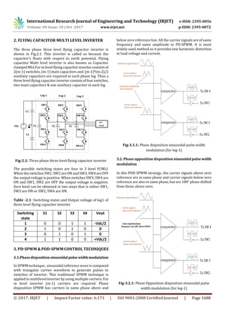
Harmonic Analysis of Three level Flying Capacitor Inverter
Mohd Esa1, Mohd Abdul Muqeem Nawaz2 & Syeda Naheed3
1,2,3M.E. Student, EED, Muffakham Jah College of Engineering and Technology, Hyderabad, India
---------------------------------------------------------------------***---------------------------------------------------------------------
Abstract –The aim of this paper is to determine the Total
harmonic distortion (THD) of three phase three level flying
capacitor inverter fed star connected R-L load. The
modulation Techniques used is Phase Disposition Sinusoidal
pulse width modulation (PD-SPWM) and Phase Opposition
Disposition Sinusoidal pulse width modulation (POD-
SPWM).The Modulation index is varied to analyze its effect on
Current THD and Voltage THD.This paper also presents the
comparison of PD-SPWM and POD-SPWM controlled Flying
capacitor Inverter in terms of THD. The simulation result
shows that PD-SPWM has betterperformance whencompared
to POD-SPWM. The simulation of circuit is done by using
MATLAB/Simulink.
Key Words: PD-SPWM, POD-PWM,THD,ModulationIndex.
1. INTRODUCTION
1.1 Multilevel Inverters
Multilevel inverters have drawn tremendous interest in
power industry owing to their advantages such as higher
efficiency, lower common modevoltage,lowervoltagestress
on power switches, lower dv/dt ratio, no EMI problems & its
suitability for high voltage and high current applications
[1].There are three types of multilevel inverters. They are
Diode clamped or Neutral clamped, Flying capacitor or
Capacitor clamped &. Cascaded Hbridgemultilevel inverters
[2]-[3].During the 1980s the development of the Multilevel
Converters did not move much forward. Onlyafterten years,
at the turn of the decade, finally appeared articlesabout new
applications, e.g. nuclear fusion, and new control methods.
The next turning point came at the beginning of the 1990s
when Meynard and Foch (1992) presented the flying
capacitor converter as a multilevel chopper and a multilevel
inverter.
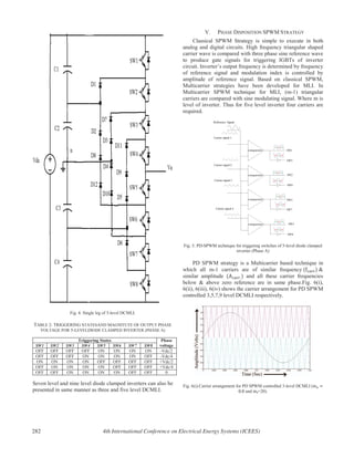
Fig-1.1.1: Classification of Multilevel Inverter
The FCMLI is considered For THD analysis in this paper
because it is easier to increase number of levels in this
inverter than the diode clamped multilevel inverters. The
advantage of FCMLI is that it can control both real and
reactive power flow.
1.2 Multilevel Inverter PWM Strategies
PWM control strategies are development to reducetheTotal
Harmonic Distortion [4].PWM strategies used in
conventional inverters can be modified to use in MLI.The
advent of multilevel inverter PWM modulation
methodologies can be classified according to switching
frequency as shown in figure 1.2.1
Fig-1.2.1: Classification of Multilevel Inverter PWM
Strategies
There are several Multi carrier based High frequency
techniques such as i) Phase disposition PWM (PDPWM) ii)
Phase Opposition DispositionPWM (PODPWM)iii)Alternate
Phase Opposition Disposition PWM (APODPWM) iv) Phase
Shift PWM (PSPWM) v) Alternate Phase Shift PWM
(APSPWM) vi) CarrierOverLapPWM(COPWM)vii)Variable
Frequency PWM (VFPWM) viii) Alternate Variable
Frequency PWM (AVFPWM).In multilevel Inverters
modulation index is defined as follows
In this Paper, PD and POD SPWM strategies are considered
for triggering switches of three level flying capacitor
inverter.](https://image.slidesharecdn.com/ilovepdfmerged40-200326112403/85/Multilevel-Inverter-and-Multipliers-19-320.jpg)
![International Research Journal of Engineering and Technology (IRJET) e-ISSN: 2395-0056
Volume: 04 Issue: 10 | Oct -2017 www.irjet.net p-ISSN: 2395-0072
© 2017, IRJET | Impact Factor value: 6.171 | ISO 9001:2008 Certified Journal | Page 1693
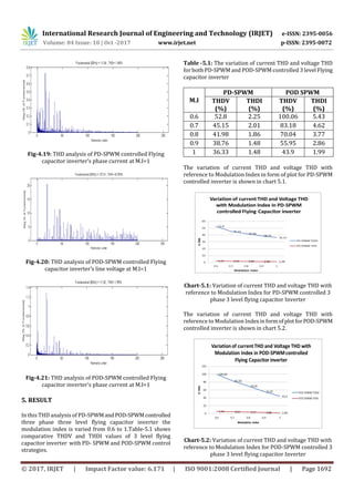
From the chart 5.1 and 5.2 it is observed that as the
modulation index increases both current THD and Voltage
THD decreases. The comparison of voltage THD for PD-
SPWM and POD-SPWM controlled 3 phase 3 level flying
capacitor inverter is shown in chart 5.3 & the comparison of
current THD for PD-SPWM and POD-SPWM controlled 3
phase 3 level flying capacitor inverter is shown in chart 5.4
Chart-5.3: Comparison of voltage THD’s for PD-SPWM &
POD-SPWM controlled 3 level Flying capacitor inverter
Chart-5.4: Comparison of current THD’s for PD-SPWM &
POD-SPWM controlled 3 level Flying capacitor inverter
6. CONCLUSION
A three phase three level flying capacitor inverter has been
implemented with PD-SPWM and POD-SPWM control
strategies. Analysis of current THD and voltage THD is done
at Modulation index from 0.6 to 1(Unity). Simulation results
of PD-SPWM controlled flying capacitor inverter and POD
SPWM controlled flying capacitor inverter are compared.
From chart 5.3 and chart 5.4 it can be concluded that PD-
SPWM provides better quality of output voltage and current
when compared to POD-SPWM controlled inverter i.e. both
current THD and voltage THD is lesser in case of PD-SPWM.
REFERENCES
[1] Muhammad H. Rashid-“Power Electronics-Circuits,
Devices and Applications” Pearson Education Incorporated,
2005.
[2] Tolbert. L. M and Pend. F. Z -“Multilevel Converter as a
Utility Interface forRenewableEnergySystems”,IEEEPower
Engineering Society Meeting, Vol. 2, pp. 1271- 1274, 2000.
[3]BK Bose-“Power electronics-An emerging technology”
IEEE Transactions on Industrial Electronics, vol.36,no.3, pp.
403–12, Aug 1989.
[4] Mohd Esa and Mohd Abdul Muqeem Nawaz, "THD
analysis of SPWM & THPWM ControlledThreephaseVoltage
Source Inverter", International Research Journal of
Engineering and Technology (IRJET), vol.04,no.10,pp.391-
398, 2017.
BIOGRAPHIES
Mohd Esa is currently pursuing M.E.
(Power Electronics systems) from
Muffakham Jah CollegeofEngineeringand
Technology, Hyderabad. He Received his
B.E degree from Osmania University,
Hyderabad. He is Member of International
Association of Engineers (IAENG), Hong
Kong. His research of interests includes Multi level
inverters and electric drives.
Mohd Abdul Muqeem Nawaz, was Born in
Hyderabad, India in 1994.He received his
B.E degree from Osmania University;Heis
currently pursuing M.E (Power
Electronics systems) from Muffakham Jah
College of Engineering and Technology,
Hyderabad. He is Member of International
Association of Engineers (IAENG), HongKong. Hisresearch
interests include power electronics, FACTS devices and
power electronics applications to power systems.](https://image.slidesharecdn.com/ilovepdfmerged40-200326112403/85/Multilevel-Inverter-and-Multipliers-25-320.jpg)

![Common Mode Voltage reduction in Diode Clamped
MLI using Phase Disposition SPWM Technique
Mr.Mohd Esa
M.E. Student, Department of Electrical Engg.
M.J.C.E.T., Hyderabad, India
zmohdesa@gmail.com
Mr.J.E.Muralidhar
Associate Professor, Department of Electrical Engg.
M.J.C.E.T., Hyderabad, India
muralidhareed@mjcollege.ac.in
Abstract—The aim of this paper is to reduce the Common
Mode Voltage (CMV) in the Diode Clamped Multilevel Inverter
(DCMLI).Three phase star connected RL load is connected to
DCMLI. The common mode voltage exists between star point of
load & system ground. Premature failure of bearings of
Induction Motor (IM) is caused by CMV and is necessary to
reduce. In this paper, Phase Disposition Sinusoidal Pulse Width
Modulation (PD SPWM) technique is used for reduction of CMV
and LC filter is used for reduction of Harmonics.MATLAB
Simulink is used for the simulation of circuit. Total Harmonic
Distortion (THD) and CMV are investigated.
Keywords—CMV,THD,PD SPWM,DCMLI
I. INTRODUCTION
In high power & high voltage applications, Multilevel
Inverters (MLI) have attracted more attention due to their
advantages such as lesser CMV, lesser voltage stress on
switches and low dv/dt ratio [1].The conventional pulse width
modulated voltage source inverter has the problem of presence
of more harmonics when compared to multilevel inverters.
They main drawback of CMV is that it give rise to shaft
voltage & bearing currents [2], [3].CMV and THD must be
reduced for better operation of IM drives. Some methods for
reduction of CMV are application of common mode choke,
dual bridge inverters [4], four leg inverters [5], & improved
modulation strategies [6].CMV can be reduced in MLI by
applying proper control strategy. Switching states in MLI is
more in number so the output voltage is stepped in smaller
increments. This mitigates harmonics at low switching
frequencies thus decreasing the losses in switches. Leakage
current gets decreased as dv/dt is low in MLI.CMV gets
reduced in MLI, which avoids failure of bearing [7].
The concept of multilevel began with the 3- level converter
which is often known as neutral point converter. Here
converter refers to the power flow in both the directions i.e.
from D.C. to a.c. called as inverter and from a.c. to D.C. called
as rectifier. The commercially existing MLI types are Diode
Clamped (DC-MLI) or Neutral-Point Clamped (NPC-MLI)
[8], Flying Capacitor (FC-MLI) or Capacitor Clamped &
Cascaded H-bridge multilevel inverter (CHB-MLI). Though
CHB-MLI was invented in 1975 it found its application in
1990, hence DC-MLI was considered as first generation of
multilevel inverters. DC-MLI was the first one that made it
possible to produce an output voltage from only one D.C.
source. All devices in DC-MLI are switched at the
fundamental frequency thus its efficiency is high & when
number of levels of DC-MLI increases, harmonic content in
output voltage gets low enough to avoid need of filters but
disadvantage of DC-MLI is requirement of excessive
clamping diodes when numbers of levels are high.
The Flying Capacitor Multilevel Inverter is an alternative
to DC-MLI.Flying capacitor MLI uses capacitors for
clamping.FC-MLI is used in various high power applications
because it is easy to increase number of levels in FC-MLI than
the DC-MLI.For m-level, flying capacitor inverter consists of
2× (m-1) switches, (m-1) main capacitors and (m-1) × (m-2)/2
auxiliary capacitors in each leg [9].FC-MLI can control both
active & reactive power flow but for active power
transmission, switching frequency & switching losses are
more.
Cascaded H-bridge MLI is also recognized as Multicell
inverter. In CHB-MLI topology output voltage is the sum of
all of the individual H-bridge outputs because a.c. output of
each H-bridge is connected in series [10]. For m-level inverter
number of cells required is (m-1)/2.The components used are
less, because clamping diodes or clamping capacitors are not
required in this topology. The drawback of CHB-MLI is that
each H-bridge requires separate D.C. sources.
Inverter’s output voltage can be controlled by various
modulation techniques. The classifications of these techniques
are based on fundamental switching frequency and high
switching frequency. Modulation techniques based on
fundamental switching frequencies are Space Vector Control
& Selective Harmonic Elimination [11]. High switching based
methods are Sinusoidal Pulse Width Modulation (SPWM),
Selective Harmonic Elimination (SHE-PWM), Space Vector
Modulation (SVM).These PWM techniques are easy to
implement and control, and they reduce lower order
harmonics.SPWM is simplest of all the above techniques. In
1964, SPWM was introduced by schonung and
stemmler.SPWM technique does not require any computations
and is very popular in industrial applications.Multi carrier
techniques based on classical SPWM has been developed.
279978-1-5386-3695-4$31.00 c 2018 IEEE](https://image.slidesharecdn.com/ilovepdfmerged40-200326112403/85/Multilevel-Inverter-and-Multipliers-27-320.jpg)
![Phase shifting and level shifting are major techniques of
Multicarrier SPWM. The Multi carrier based High frequency
techniques are
Phase Shift PWM (PSPWM)
Alternate Phase Shift PWM (APSPWM)
Phase Disposition PWM (PDPWM)
Phase Opposition Disposition PWM (PODPWM)
Alternate Phase Opposition Disposition PWM
(APODPWM)
Carrier Over Lap PWM (COPWM)
Variable Frequency PWM (VFPWM)
Alternate Variable Frequency PWM (AVFPWM).
These techniques are helpful to reduce THD and CMV
in multilevel inverters [6]. In this paper, CMV and THD
reduction in DCMLI using PDSPWM is presented.
II. COMMON MODE VOLTAGE
A. Definition:
Voltage that exists between neutral-point of wye
connected load & system ground is known as common mode
voltage (or) voltage between star point of load and input D.C.
midpoint (or) The CMV is defined as the voltage potential
difference between the mid-point of the D.C. link capacitors
and the star point of the load network. Mathematical
expression for CMV is shown in equation (1).
(1)
Where , , are the phase voltages. is common
mode voltage. A generalized drive system is represented in
fig. 1.
Fig.1. A generalized drive system
It has been observed that each switching state has its own
related CMV level.CMV has different values of ± 6 or
± for conventional three phase two level inverter based
on the inverter’s switching state selected.
B. Effects of common mode voltage:
a) Regardless of number of legs & levels, high
amplitude & high frequency CMV exists always in
pulse width modulated inverters because of its
switching operation which results in common mode
current (CMC) through parasitic capacitors between
inverter, loads & ground respectively. This CMC
cause’s mal operation of inverter control system as it
is a source of EMI noise.
b) Shaft voltages on the rotor are caused by pulse width
modulated inverters because of CMV.Premature
failure of IM bearings is caused when this shaft
voltage exceeds the voltage limit of bearings
lubricant.CMV is required to reduce by choosing
specific reduction technique.
C. Reduction methods for common mode voltage:
Few methods to combat CMV are represented in fig.2.
Fig. 2.CMV reduction techniques
Extra leg is used in four leg inverter which is connected to star
point of load to reduce CMV but in four leg inverter switching
scheme becomes complex. In reducing electromagnetic
interference, eliminating CMV and bearing currents of motor
the Dual Bridge Inverter (DBI) topology is more effective. In
DBI topology, two parallel inverters with reverse polarities is
connected to double winding motor to eliminate CMV.Size
and cost are disadvantage for this CMV reduction technique.
In this paper, Multicarrier based Phase Disposition SPWM
technique is used to reduce CMV.
280 4th International Conference on Electrical Energy Systems (ICEES)](https://image.slidesharecdn.com/ilovepdfmerged40-200326112403/85/Multilevel-Inverter-and-Multipliers-28-320.jpg)
![III. TOTAL HARMONIC DISTORTION
THD is the measure of effective value of harmonic
components of a distorted waveform. Presence of nonlinear
devices in power system is cause of harmonic distortion.IEEE
Standard 519-1992 recommends the requirements for
harmonic control in electrical power systems. Inverter’s output
voltage quality strongly related to total harmonic distortion. A
mathematical expression for THD is shown in equation (2).
(2)
Where h is harmonic order, is harmonic voltage, and is
fundamental voltage. To do the THD analysis of output
voltage of inverter Fast Fourier transform (FFT) is used. The
algorithm requires a large amount of calculations but with
MATLAB simulation software, calculations are done easily.
In this paper THD is also reduced along with CMV in PD
SPWM controlled DCMLI.
IV. DIODE CLAMPED MULTILEVEL INVERTER
In 1981,DCMLI was proposed by Nabae et al., DC-MLI is
also known as Neutral-Point Clamped Inverter (NPC-MLI)
[8].The m-level inverter leg contains (m-1) D.C. bus
capacitors, 2×(m-1) switches & required clamping diodes are
(m-1) × (m-2).
A. 3-level Diode clamped Inverter
Power circuit of single leg of 3- level DCMLI is shown in
fig. 3. In each leg it requires 4 switches. Total of twelve
switches are required in three phase 3 level DCMLI. SW1,
SW2 are IGBTs in upper half of the first leg and SW3, SW4
are IGBTs in lower half of the first leg and it has two
clamping diodes in each leg. Main capacitors required are two.
The operation of 3-level DCMLI is as follows. When switch
SW1, SW2 are ON and SW3, SW4 are OFF output phase
voltage is /2.When SW2, SW3 are ON and SW1, SW4 are
OFF output phase voltage is zero. When SW3 and SW4 are
ON and SW1, SW2 are OFF output phase voltage is /2.
Table 1 shows the triggering states and output phase voltage
magnitude for phase A of 3- level diode clamped inverter.
Requirement of the clamping diodes increases as inverter’s
output voltage level increases which makes this topology
bulky.
TABLE 1: TRIGGERING STATES AND MAGNITUTE OF OUTPUT PHASE
VOLTAGE FOR 3-LEVEL DIODE CLAMPED INVERTER (PHASE A)
Triggering States Phase
VoltageSW1 SW2 SW3 SW4
OFF OFF ON ON -Vdc/2
OFF ON ON OFF 0
ON ON OFF OFF +Vdc/2
Fig. 3. Single leg of 3- level DCMLI.
B. 5-level Diode clamped Inverter
Power circuit of single leg of 5-level DCMLI is shown
in Fig.4.It needs eight switches in each leg. There are total 24
switches in three phase five level DCMLI.SW1, SW2, SW3 &
SW4 are IGBTs in upper half of the first leg and SW5, SW6,
SW7 & SW8 are the IGBTs in lower half of the first leg, five
level diode clamped inverter has 12 clamping diodes in each
leg. Main capacitors required are four. Thus for three phase
five level DCMLI has 36 clamping diodes. Table 2 shows
triggering states to synthesize five level phase output voltage.
The steps to produce the 5- level phase voltages are as
follows.
Switch ON,IGBTs from SW1 to SW4 for an output
phase voltage
Switch ON, IGBTs from SW2 to SW5 for an output
phase voltage
Switch ON, IGBTs from SW3 to SW6 for an output
phase voltage
Switch ON, IGBTs from SW4 to SW7 for an output
phase voltage
Switch ON, IGBTs from SW5 to SW8 for an output
phase voltage
4th International Conference on Electrical Energy Systems (ICEES) 281](https://image.slidesharecdn.com/ilovepdfmerged40-200326112403/85/Multilevel-Inverter-and-Multipliers-29-320.jpg)
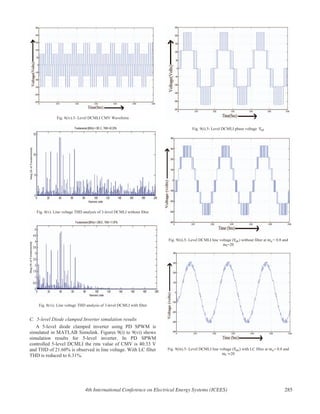
![Fig. 11(iv).9-Level DCMLI CMV waveform
Fig. 11(v).Line voltage THD analysis of 9-level DCMLI without filter
Fig. 11(vi).Line voltage THD analysis of 9-level DCMLI with LC filter
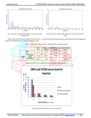
Table 3 shows the CMV and %THD for two level VSI, 3, 5, 7
and 9 level Diode clamped Inverter using Phase Disposition
SPWM technique with and without LC filter.
TABLE 3: CMV AND %THD VALUES FOR PD SPWM CONTROLLED
DCMLI
2-level
VSI
3-Phase PD SPWM Controlled DCMLI
3-level 5-level 7-level 9-level
CMV
(V)
145.2 81.68 40.33 25.66 17.06
THD
(%)
Without
filter
97.63 42.23 21.60 13.76 10.97
With
filter
28.02 11.97 6.31 4.28 3.52
Variation of CMV and % THD with level of Inverter is shown
in fig. 12.
Fig.12.Variation of CMV and THD with level of Inverter
From the fig. 12 it can be witnessed that as CMV and %THD
reduces with increase in inverter’s level, nature of output
voltage gets improved which reduces total harmonic distortion
by decreasing lower order harmonics. Table 3 clearly shows
that as the level of inverter increases, number of steps in
output voltage increases which reduces CMV.
VII. CONCLUSION
Diode clamped multilevel inverter for three, five, seven and
nine level using PD SPWM is simulated in Matlab/Simulink
software.Table-3 evidently shows that two level inverter
produces high %THD & CMV which causes high leakage
current & premature failure of IM bearing. From simulation
results it can be concluded that CMV can be reduced in
DCMLI by employing PD-SPWM strategy. DCMLI reduces
CMV by reducing dv/dt in output voltage and thus flow of
leakage current in motor gets reduced [12].
288 4th International Conference on Electrical Energy Systems (ICEES)](https://image.slidesharecdn.com/ilovepdfmerged40-200326112403/85/Multilevel-Inverter-and-Multipliers-36-320.jpg)
![APPENDIX
MATLAB/Simulink Parameters:
1. Input Voltage =440V
2. Load R=100 Ohms, L=50e-3 Henry
3. System frequency=50Hz
4. Switching frequency
5. Amplitude Modulation Index 0.8
6. Frequency Modulation Index
7. LC filter: L=5.7e-3 Henry, C=3.45e-6 Farad
REFERENCES
[1] M.H. Rashid,“Power Electronics Circuits, Devices & Applications”
Pearson Education Incorporated, 2005.
[2] Jay M.Erdman,R.J.Kerkman,D.W.Schlegel & G.L.Skibinski , “Effect
of PWM Inverters on A.C. Motor Bearing currents and Shaft voltages,”
I.E.E.E. Trans. on Ind. App., Vol.32, No. 2 , pp.250-
259,MAR/APR,1996.
[3] Doyle Busse,Jay Eradman,R.J.Kerkman,Dave Schlegel & Gary
Skibinski , “System Electrical Parameters and their effects on Bearing
currents,” I.E.E.E. Trans. on Ind. App. ,Vol.33, No.2, pp. 577-583,
MAR/APR ,1997.
[4] R.S. Kanchan, P.N. Tekwani, M.R. Baiju, K. Gopakumar and A. Pittet,
“3-level Inverter configuration with Common Mode Voltage elimination
for Induction Motor Drive,” I.E.E. Proceedings- Elec. Power App., Vol.
152, No. 2, pp.261-270, MAR 2005.
[5] Alexander L. Julian, Giovanna Oriti, and Thomas A. Lipo, “Elimination
of Common Mode Voltage in 3-Phase Sinusoidal Power Converters,”
I.E.E.E. Transactions on Power Electronics Vol.14,No.5 , pp.982-989
,SEPT 1999.
[6] M.M.Renge and H.M.Suryawanshi , “ Multilevel Inverter to Reduce
Common Mode Voltage in A.C. Motor Drives Using SPWM
Technique.” pp.21-27,Journal of Power Electronics, Vol. 11, No. 1, JAN
2011.
[7] M.M.Renge and H.M.Suryawanshi , “5-Level Diode Clamped Inverter
to Eliminate Common Mode Voltage & Reduce dv/dt in Medium
Voltage Rating Induction Motor Drives.”, I.E.E.E. Trans. on Power
Electronics ,Vol.23 , No. 4 , pp.1598-1607,JUL,2008.
[8] A.Nabae, I. Takahashi, H.Akagi‘A new Neutral Point CIamped PWM
Inverter’’ I.E.E.E. Trans. on Ind. App., Vol. IA-I7, No.5,pp.518-52
SEPT/OCT,1981.
[9] T. A Meynard, H. Foch, “Multilevel conversion: High voltage Choppers
& voltage source inverters”,I.E.E.E.-Power Electronics Specialists Conf.
Rec., pp.397-403,1992.
[10] P. W. Hammond, “A new approach to enhance power quality for
medium voltage A.C. drives”,I.E.E.E. Trans. on Ind. App., vol. 33, no. I,
pp. 202-208, JAN./FEB 1997.
[11] M.H.Rashid,“Power Electronics Hand book ” , Edition,Butterworth-
heinemann,pp.399-400
[12] Atanda k Raji and Mohamed T E Kahn, “Investigation of common
mode voltage and ground leakage current of grid connected transformer
less PV inverter topology” Journal of Energy in Southern Africa ,Vol 26
No 1 February 2015.
4th International Conference on Electrical Energy Systems (ICEES) 289](https://image.slidesharecdn.com/ilovepdfmerged40-200326112403/85/Multilevel-Inverter-and-Multipliers-37-320.jpg)
![Mr.Mohd Esa
M.E. Student, Electrical Engg. Dept.
Muffakham Jah College of Engg. & Tech.
Hyderabad, India
zmohdesa@gmail.com
Mr.J.E.Muralidhar
Associate Professor, Electrical Engg. Dept.
Muffakham Jah College of Engg. & Tech.
Hyderabad, India
muralidhareed@mjcollege.ac.in
Abstract—This paper aims to reduce the Common Mode
Voltage (CMV) in the Diode Clamped Multilevel Inverter
(DCMLI). Three phase wye connected R-L load is connected to
DCMLI. The common mode voltage exists between neutral point
of wye connected load and ground of system.CMV causes
premature failure of bearings of induction motor & is essential to
reduce.CMV is reduced in this paper by using Phase Opposition
Disposition SPWM technique. A comparative study of three, five,
seven and nine level DCMLI in terms of THD and CMV has been
presented. The effect of a passive LC filter on THD was
studied.The simulation of circuit is carried out by using
MATLAB/Simulink. Simulation result showed reduction in THD
and CMV by using POD-SPWM controlled higher level
Inverters.
Keywords—CMV,THD,POD SPWM,DCMLI
I. INTRODUCTION
Inverter converts D.C. input voltage to a.c. output
voltage of desired magnitude and frequency [1]-[4]. The two-
level inverter can create only two different output voltages
i.e.,+ V /2 or −V /2 when inverter’s D.C. input voltage is
V . The concept of Multilevel Inverter (MLI) does not depend
on just two levels of voltage to create an a.c. signal. Instead
several levels of voltages are added to each other to create a
smoother stepped waveform. High speed switching is used in
MLI [5]. MLI found its applications in industrial motor drives,
utility interfaces for renewable energy systems, flexible a.c.
transmission systems(FACTS), high voltage direct current
transmission (HVDC), and traction drives systems [6]-[9]. The
advantages of multilevel Inverters when compared with
conventional 2-level converter are less harmonic distortion in
output voltages, low dv/dt [10].CMV is less in MLI when
compared to two level VSI.CMV results in high leakage
current and premature failure of motor bearing take place so it
is required to reduce. Various modulation strategies based
methods to reduce CMV are MLI using Active Zero State
PWM (AZSPWM) [11],MLI using Remote State PWM
(RSPWM) [12],MLI using Near State PWM (NSPWM)
[13],MLI using SPWM technique[14],MLI using Space vector
modulation[15] and MLI using Modified space vector
modulation topology. Extra hardware circuitry based methods
to reduce CMV are
• Dual bridge inverter
• Four leg Inverter
• Properly designed dv/dt filter &
• Common mode chokes.
The concept of multilevel inverters (MLI) has been
introduced since mid-1970. The term multilevel coined with
the three level inverter. Afterwards, numerous multilevel
inverter topologies continue to develop, especially in the last
two decades. There are several types of multilevel Inverters.
The three main types of multilevel Inverters are Diode
Clamped Multilevel Inverter (DC-MLI), Flying Capacitor
Multilevel Inverter (FC-MLI) or Capacitor clamped MLI and
Cascaded H-bridges multilevel Inverter (CHB-MLI). First
multilevel inverter (MLI) was cascaded H bridge inverter
designed in 1975 but it found its application in 1990, therefore
DC-MLI was considered as first generation of multilevel
technology. The advantages of DC-MLI are as follows:
• Inverter efficiency is high because all devices are
switched at fundamental frequency.
• Harmonic content in output voltage is low when
compared to conventional two level inverter.
• The capacitance requirement of the inverter is
lessened due to all phases sharing a common DC
link.
• The control method is simple.
DC-MLI requires excessive clamping diodes when number of
levels is high and it is difficult to control the real power flow
of individual converter in multi converter systems. DC-MLI
founds its applications in High power medium voltage
variable speed drives, interface between HVDC transmission
line and a.c. transmission line.
In 1992, Meynard and Foch proposed flying capacitor MLI.
The structure of this inverter is similar to that of the DC-MLI
Common Mode Voltage reduction in Diode
Clamped MLI using Phase Opposition Disposition
SPWM Technique
International Conference on Electrical, Electronics, Computers, Communication, Mechanical and Computing (EECCMC)
Page 355 of 470
978-1-5386-4304-4/18/$31.00 ©2018 IEEE](https://image.slidesharecdn.com/ilovepdfmerged40-200326112403/85/Multilevel-Inverter-and-Multipliers-38-320.jpg)
![except that instead of using clamping diodes, it uses capacitors
as its name implies. This topology has a ladder structure of
D.C. side capacitors, where the voltage on each capacitor
differs from that of the next capacitor. The voltage increment
between two adjacent capacitor legs gives the size of the
voltage steps in the output waveform. For, m level flying
capacitor inverter 2×(m-1) switches, (m-1) main capacitors
and (m-1)×(m-2)/2 auxiliary capacitors are required in each
leg[21].The advantages of FC-MLI are as follows:
• Large amount of storage capacitors can provide
capabilities during power outages.
• Like the Diode clamped inverter with more levels,
the harmonic content is low.
• Both real and reactive power flow can be controlled.
FC-MLI needs excessive number of storage capacitors when
number of levels is high. High level inverters are more
difficult to package with bulky power capacitors & are more
expensive, Inverter control is difficult & are expensive too.
Efficiency is reduced for real power transmission.
Fig.1. Classification of Inverters
The third topology is Cascaded H bridge multilevel
inverter. The cascaded multilevel inverter is based on the
series connection of single leg or double leg (H bridges)
inverters with separate D.C. sources. The a.c. output of each
H-bridge is connected in series such that the synthesized
output voltage is the sum of all of the individual H-bridge
outputs. For m-level inverter number of cells required is (m-
1)/2. The advantages of CHB-MLI are as follows:
• Less components are required in CHB-MLI when
compared with DC-MLI and FC-MLI to achieve
same number of voltage levels.
• In order to reduce switching losses & device stress
soft switching techniques can be used.
CHB-MLI requires separate D.C. sources for real power
conversions, there by restricting its applications.
Different modulation techniques exist to control the
output voltage of inverter. The modulating signal based
techniques are Sinusoidal PWM, Third harmonic injection
PWM,Space vector PWM and Modified space vector
PWM.The Multicarrier PWM techniques are Phase
Disposition PWM,Phase Opposition Disposition
PWM,Alternative Phase Opposition Disposition PWM.
Fig.2. Classification of Modulation Techniques
In this paper,Common Mode Voltage and Total Harmonic
Distortion reduction in DC-MLI using Phase Opposition
Disposition Sinusoidal Pulse Width Modulation is presented.
II. COMMON MODE VOLTAGE
The common mode voltage is defined as the potential of
the star point of the load with respect to the center of the D.C.
bus of the inverter (or) The common mode voltage (CMV) of
the three-phase system is defined as the voltage potential
difference between the star point of the load network and the
mid-point of the D.C. link capacitors (or) Common mode
voltage is voltage between neutral point of star connected load
and system ground. Mathematical expression for CMV is
shown in equation (1).
CMV = V = (1)
Where V ,V , V are the voltages between ground to phase.
V is voltage between neutral of motor and system ground. A
generalized drive system is represented in fig. 3.
Fig.3. A generalized drive system
International Conference on Electrical, Electronics, Computers, Communication, Mechanical and Computing (EECCMC)
Page 356 of 470](https://image.slidesharecdn.com/ilovepdfmerged40-200326112403/85/Multilevel-Inverter-and-Multipliers-39-320.jpg)
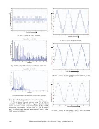
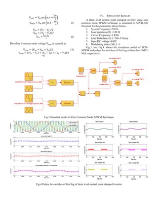
![Table 2 shows the CMV and %THD for two level VSI, 3, 5, 7
and 9 level Diode clamped Inverter using Phase Opposition
Disposition SPWM technique with and without LC filter.
TABLE 2: CMV AND %THD VALUES FOR POD SPWM CONTROLLED
DCMLI
2-level
VSI
3-Phase POD SPWM Controlled DCMLI
3-level 5-level 7-level 9-level
CMV
(V)
145.2 44.3 18.76 12.56 12.20
THD
(%)
Without
filter
97.63 70.46 35.65 22.46 13.86
With
filter
28.02 21.79 11.21 7.19 4.56
Variation of CMV and % THD with level of Inverter is shown
in fig. 12.
Fig.12.Variation of CMV and THD with level of Inverter
From the fig. 12 it can be noticed that CMV and %THD
decreases with increase in level of the inverter as increase in
level improves the nature of output voltage waveform,
approaching to sinusoidal shape which in turn reduces lower
order harmonics. The number of steps in the output voltage
increases as the level increases which reduces rate of rise of
voltage.CMV and %THD reduces as step size reduces.
VII. CONCLUSION
POD SPWM controlled DCMLI for three, five, seven and nine
level is simulated in Matlab/Simulink software.Table-2 clearly
shows that two level inverter produces high CMV and THD
which causes high leakage current and premature failure of
motor bearing . A comparative study of three level, five level,
seven level and nine level DCMLI in terms of THD and CMV
shows as level of the inverter increases CMV and %THD
decreases. The simulation output gives a conclusion that by
employing POD SPWM technique to DCMLI, CMV can be
reduced. POD SPWM controlled DCMLI also reduces dv/dt
in its output voltage and therefore CMV and thus flow of
leakage current in motor bearing reduced.
APPENDIX
Parameters Used for Simulation:
1. Input D.C.Voltage V =440V
2. Load R=100 Ohms, L=50e-3 Henry
3. Fundamental frequency=50Hz
4. Carrier frequency f = 1000Hz
5. Amplitude Modulation Index, m = 0.8
6. Frequency Modulation Index, m = 20
7. LC filter: L=5.7e-3 Henry, C=3.45e-6 Farad
REFERENCES
[1] G. Prem Sunder, B. Shanthi, A. Lamehi Nachiappan and S. P. Natrajan,
“Performance Analysis of modified CHB MLI using various carrier
modulation schemes”, IJESA, vol. 3, no. 5, (2013), pp. 310-316.
[2] F. Z. Peng and J. S. Lai, “Multilevel converters, A new breed of power
Electronics converters”, IEEE Trans Industries Application, vol. 32,
(1996), pp. 509-517.
[3] K. Jagdish, “THD Analysis for different levels of cascade multilevel
inverter for industrials applications”, IJETAE, (2012), pp. 20-30.
[4] M. Kavitha, A. Arunkumar, N. Gokulnath and S. Arun, “New cascaded
H-bridge multilevel inverter topology with reduced number of switches
and sources”, JEEE, vol. 2, no. 6, (2012), pp. 26-36.
[5] D. Grahame Holmes, Thomas A. Lipo, “Pulse Width Modulation For
Power Converters”, WILEY INTERSCIENCE,2003.
[6] Michail Vasiladiotis, “Analysis, Implementation and Experimental
Evaluation of Control Systems for a Modular Multilevel Converter”,
Master Thesis, KTH-EME, 2009.
[7] Zhang Jingzhe, “Analysis of a Cascade Voltage Source Multilevel
Converter for a High Power Motor Drive”,Master Thesis, KTH-EME,
2008.
[8] Cristian Sandu, Nicoleta Carnu and Valentin Constantin Costea,
“Medium Voltage Modular Multi-Level Inverter”, Master Thesis,
Aalborg University, 2008.
[9] A. Antonopoulos, L Ängquist and H.P. Nee, “On Dynamics and
Voltage Control of the Modular Multilevel Converter”, European Power
Electronics Conference (EPE), Barcelona, Spain, September 8-10, 2009
[10] A. Mokhberdoran and A. Ajami, “Symmetric and Asymmetric Design
and Implementation of New Cascaded Multilevel Inverter Topology”,
IEEE Transactions on Power Electronics, vol. 29, no. 12, pp. 6712-6724,
2014.
[11] Y.S. Lai and F.S. Shyu, “Optimal common-mode voltage reduction
PWMtechnique for inverter control with consideration of the dead-time
effects-part I:basic development,” IEEE Trans. on Industry Applications,
vol 40, pp.1605-1612, November/December 2004.
[12] M. Cacciato, A. Consoli, G. Scarcella, and A. Testa, “Reduction of
commonmode currents in PWM inverter motor drives,” IEEE Trans. on
Industry Applications, vol. 35, pp. 469-476, March/April 1999.
[13] E. Ün and A.M. Hava, “A near state PWM method with reduced
switching frequency and reduced common mode voltage for three-phase
voltage source inverters,” in Proc. IEEE-IEMDC’07, 2007, pp. 235-240.
[14] P. G. Shewane, S. Gaigowal, B. Rane, “Multicarrier Based SPWM
Modulation for Diode Clamped MLI to reduce CMV and THD”,
Power,Automation and Communication [INPAC-2014], International
Conference at Amravati on 6-8 OCT.2014, pp. 50-
54,DOI:10.1109/INPAC.2014.6981134, IEEE.
[15] Sk. Moin Ahmed, Haitham Abu-Rub, Zainal Salam, “Common Mode
Voltage Elimination in a Three-to-Five-Phase Dual Matrix Converter
Feeding a Five-Phase Open-End Drive Using Space-Vector Modulation
Technique”,IEEE TRANSACTIONS ON INDUSTRIAL
ELECTRONICS,VOL. 62, NO. 10, OCTOBER 2015.
International Conference on Electrical, Electronics, Computers, Communication, Mechanical and Computing (EECCMC)
Page 364 of 470](https://image.slidesharecdn.com/ilovepdfmerged40-200326112403/85/Multilevel-Inverter-and-Multipliers-47-320.jpg)
![www.ijcrt.org © 2018 IJCRT | Volume 6, Issue 2 April 2018 | ISSN: 2320-2882
IJCRT1812942 International Journal of Creative Research Thoughts (IJCRT) www.ijcrt.org 579
Common Mode Voltage reduction in Diode Clamped
MLI using Alternative Phase Opposition Disposition
SPWM Technique
1
Mohd Esa, 2
J.E.Muralidhar
1
M.E. Student, 2
Associate Professor
1,2
Electrical Engineering Department
1, 2
Muffakham Jah College of Engineering and Technology, Hyderabad, India
Abstract: The main objective of this paper is to reduce the Common Mode Voltage (CMV) in the Diode Clamped Multilevel Inverter
(DCMLI).Three phase Y-connected RL load is connected to DCMLI. The common mode voltage exists between neutral point of Y-
connected load and system ground.CMV causes premature failure of bearings of induction motor and is essential to reduce. In this
paper, Alternative Phase Opposition Disposition SPWM technique is used to reduce common mode voltage. Two level, five level,
seven level and nine level DCMLI are compared in terms of THD and CMV.The effect of a passive LC filter on THD was studied.
The simulation of circuit is carried out by using MATLAB/Simulink. Simulation result portrays reduction in THD and CMV by using
APOD-SPWM controlled higher level Inverters.
IndexTerms - CMV, THD, APOD SPWM, DCMLI
I. INTRODUCTION
CMV is define as voltage between neutral point of the load and the dc midpoint or the voltage between neutral point of load and the
system ground or the common mode voltage is defined as the potential of the star point of the load with respect to the center of the D.C.
bus of the inverter (or) the common mode voltage (CMV) of the 3-phase system is defined as the voltage potential difference between
the star point of the load network and the mid-point of the D.C. link capacitors[1].
CMV= ∑ (1)
Where are the voltages between ground to phase.CMV is zero in purely sinusoidal three phase system but VSI is non-
pure sinusoidal system thus it develops CMV. CMV results in high leakage current and premature failure of motor bearing so it is
required to reduce [2], [3]. Some modulation techniques based approaches to reduce CMV are MLI using SPWM technique, MLI
using Space Vector PWM technique, MLI using Modified space vector modulation technique, predictive current control method, on
zero state modulation techniques. In this paper, APOD- SPWM is used to reduce common mode voltage.
Fig.1.Schematic of single pole of MLI by a
switch [5]
Fig.2.Typical output voltage of 5
level MLI [5]](https://image.slidesharecdn.com/ilovepdfmerged40-200326112403/85/Multilevel-Inverter-and-Multipliers-48-320.jpg)
![www.ijcrt.org © 2018 IJCRT | Volume 6, Issue 2 April 2018 | ISSN: 2320-2882
IJCRT1812942 International Journal of Creative Research Thoughts (IJCRT) www.ijcrt.org 580
The idea of multilevel inverters has been introduced in 1975 with invention of cascaded H-Bridge MLI.The term multilevel began
with 3- level inverter. Afterwards numerous multilevel inverter topologies have been developed .Three different MLI topologies that
have been proposed are diode clamped or neutral point clamped, flying capacitor and cascaded H-Bridge or multicell MLI [4]. In
addition, several control strategies have been developed. The series connected capacitors constitute the energy tank for the inverter,
providing some nodes to which MLI can be connected. Each capacitor has the same voltage ,which is given by
(2)
Where m denotes the number of levels. The term level refers to number of nodes to which the inverter can be accessible. An m-level
inverter needs m-1 capacitors. Figure 2 shows the schematic of a pole in MLI.Pole is regarded as a single-pole, multi-throw switch.
Desired output can be obtained by connecting the switch to one node at a time.
Different modulation techniques exist to trigger switches of inverter circuit. The commonly used modulation techniques are as
follows
Sinusoidal pulse width modulation (SPWM) [6]
Third harmonic PWM (THPWM)
Space vector PWM (SVPWM) [7]
Modified Space vector PWM (MSVPWM)
The most popular method of controlling inverter‟s output voltage is SPWM technique.SPWM is a carrier based pulse width
modulation method in which predefined modulation signal is used to determine output voltages. Sinusoidal modulation signal is used
in SPWM technique. The gating signal in SPWM is generated by comparing a reference signal of sine shape with a triangular carrier
wave.
Fig.3.Comparision of reference and carrier signal in SPWM generation
The width of each pulse varied proportionally to amplitude of a sine wave. The output frequency of a inverter can be found by using
the frequency of reference signal. The rms output voltage can be controlled by modulation index and intern modulation index is
controlled by peak amplitude.SPWM method results in reduction of THD for output voltage.SPWM technique is effective modulation
technique and it does not require any additional components and eliminates lower order harmonics easily. Carrier based SPWM
techniques are classified as follows
Single carrier based SPWM technique
Multi carrier based SPWM technique
Single carrier SPWM technique is used for 2-level inverter whereas multi carrier SPWM technique is used in Multi-level
inverters. Multi carrier SPWM technique is further classified as follows
Phase shift SPWM technique
Level shifted SPWM technique
Hybrid SPWM technique
Level shifted SPWM technique is further classified as follows
Phase Disposition (PD)
Phase Opposition Disposition (POD)
Alterative Phase Opposition Disposition (APOD)
Alternative phase opposition disposition SPWM is used to reduce common mode voltage in Diode clamped MLI.](https://image.slidesharecdn.com/ilovepdfmerged40-200326112403/85/Multilevel-Inverter-and-Multipliers-49-320.jpg)
![www.ijcrt.org © 2018 IJCRT | Volume 6, Issue 2 April 2018 | ISSN: 2320-2882
IJCRT1812942 International Journal of Creative Research Thoughts (IJCRT) www.ijcrt.org 581
II. DIODE CLAMPED MULTILEVEL INVERTER
Diode clamped Inverter (DC-MLI) is also known as neutral point clamped inverter (NPC-MLI). A m level diode clamped inverter
typically consists of (m-1) capacitors on the D.C. bus and produces m levels on the phase voltage. The m- level inverter leg requires (m-
1) capacitors, 2× (m-1) switching devices and (m-1) × (m-2) clamping diodes [8].
Fig.4.Three phase 5 level DCMLI
For one phase, steps to synthesize the five level voltages are as follows.
1. Turn on all upper half switches of Limb-A i.e., from SW1 to SW4 for an output voltage level
2. Turn on three upper switches of Limb-A i.e., SW2 to SW4 and one lower switch of Limb-A i.e., SW5 for an output voltage
level
3. For an output voltage level ,turn on two upper switches SW3 and SW4 of Limb-A and two lower switches SW5 and
SW6 of Limb-A.
4. Turn on one upper switch SW4 of Limb-A and three lower switches SW5 to SW7 of Limb-A for an output voltage
level .
5. Turn on all lower half switches from SW5 to SW8 of Limb-A for an output voltage level
Table 1: Switching states of five level diode clamped inverter for phase A
Switching States Output
voltageSW1 SW2 SW3 SW4 SW5 SW6 SW7 SW8
High High High High Low Low Low Low Vdc/2
Low High High High High Low Low Low Vdc/4
Low Low High High High High Low Low 0
Low Low Low High High High High Low -Vdc/4
Low Low Low Low High High High High -Vdc/2
Seven level and nine level diode clamped inverters can also be presented in same manner as five level DCMLI](https://image.slidesharecdn.com/ilovepdfmerged40-200326112403/85/Multilevel-Inverter-and-Multipliers-50-320.jpg)
![www.ijcrt.org © 2018 IJCRT | Volume 6, Issue 2 April 2018 | ISSN: 2320-2882
IJCRT1812942 International Journal of Creative Research Thoughts (IJCRT) www.ijcrt.org 582
III. ALTERNATIVE PHASE OPPOSITION DISPOSITION SPWM STRATEGY
In APOD-SPWM technique the carrier signal of same amplitude are phase displaced from each other by 180° from its neighboring
carrier signals, This carriers are compared with sinusoidal signal for producing pulse signals to trigger gates of switches used in
DCMLI.For m-level output, (m-1) carrier signals are phase disposed by 180 degrees to its neighboring carrier waveform [9]. Fig. 6(a),
6(b), and 6(c) shows the carrier arrangement for APOD SPWM controlled 5, 7 and 9 level DCMLI respectively
Fig. 5. APOD-SPWM technique for triggering switches of five level diode clamped inverter (Phase A)
The amplitude modulation index and frequency ratio are mathematically shown in equations (3) and (4) respectively.
(3)
Where peak to peak amplitude of reference waveform or modulating signal, is peak to peak amplitude of individual carrier
frequency, m is output level of inverter.
Where frequency of carrier signal & is frequency of modulating signal.
Fig. 6(a).Carrier arrangement for APOD SPWM controlled 5-
level DCMLI ( and =20).
Fig. 6(b).Carrier arrangement for APOD SPWM controlled 7-
level DCMLI ( and =20).
Fig. 6(c).Carrier arrangement for APOD SPWM controlled 9-level DCMLI ( and =20).](https://image.slidesharecdn.com/ilovepdfmerged40-200326112403/85/Multilevel-Inverter-and-Multipliers-51-320.jpg)
![www.ijcrt.org © 2018 IJCRT | Volume 6, Issue 2 April 2018 | ISSN: 2320-2882
IJCRT1812942 International Journal of Creative Research Thoughts (IJCRT) www.ijcrt.org 587
V.CONCLUSION
APOD SPWM controlled DCMLI for five, seven & nine level is simulated in Matlab/Simulink software. It is cleared from fig. 12
that CMV and %THD decreases with increase in level of the inverter. Increase in level improves the nature of output voltage waveform,
approaching to sine shape which in turn lessens lower order harmonics. The number of steps in the output voltage increases as the level
increases which reduces rate of rise of voltage.CMV and %THD reduces as size of step reduces.
REFERENCES
[1] E. Un and A. M. Hava, “A Near State PWM Method with Reduced Switching Losses and Reduced Common Mode Voltage for
3-Phase Voltage Source Inverters,” Industry Applications, I.E.E.E. transactions on, vol. 45, pp. 782-793, 2009
[2] Min Zhang, “Investigation of Switching Schemes for 3-phase Four Leg Voltage Source Inverters”, A thesis submitted for the
degree of Doctor of Philosophy June, 2013, School of Electrical and Electronic Engineering,Newcastle University
[3] Anuradha V.Jadhav and Mrs.P.V.Kapoor, “Reduction of Common Mode Voltage using Multilevel Inverter”, Energy Efficient
Technologies for Sustainability [ICEETS],pp.586-590,06 October 2016,DOI: 10.1109/ICEETS.2016.7583822,I.E.E.E.
[4] T. Cunnyngham. Cascade Multilevel Inverters for Hybrid-Electric Vehicle Applications with Variant DC Sources. Master‟s
thesis, The University of Tennessee, 2001.
[5] Muhammad H. Rashid,“Power Electronics-Circuits, Devices and Applications” Pearson Education Incorporated, 2005.
[6] P. G. Shewane, S. Gaigowal, B. Rane, “Multicarrier Based SPWM Modulation for Diode Clamped MLI to reduce CMV and
THD”, Power,Automation and Communication [INPAC-2014], International Conference at Amravati on 6-8 OCT.2014, pp. 50-
54,DOI:10.1109/INPAC.2014.6981134, IEEE.
[7] Sk. Moin Ahmed, Haitham Abu-Rub, Zainal Salam, “Common Mode Voltage Elimination in a Three-to-Five-Phase Dual Matrix
Converter Feeding a Five-Phase Open-End Drive Using Space-Vector Modulation Technique”,IEEE TRANSACTIONS ON
INDUSTRIAL ELECTRONICS,VOL. 62, NO. 10, OCTOBER 2015.
[8] A.Nabae, I. Takahashi, H.Akagi„A new Neutral Point CIamped PWM Inverter‟‟ I.E.E.E. transactions on Industry applications, Vol.
IA-I7, No.5,pp.518-52 September/October,1981.
[9] McGrath, B.P.; Holmes, D.G.; “Multicarrier PWM strategies for Multilevel Inverters,” Industrial Electronics, I.E.E.E. transactions,
vol.49, no.4, pp. 858- 867, August 2002 ,DOI:10.1109/TIE.2002.801073](https://image.slidesharecdn.com/ilovepdfmerged40-200326112403/85/Multilevel-Inverter-and-Multipliers-56-320.jpg)
![Elimination of Common Mode Voltage in
Neutral Point Clamped MLI using ZCM-SPWM
Technique
Mohd Esa
M.E. Student, EED
M.J.C.E.T., Hyderabad
zmohdesa@gmail.com
Ahmed Maaz
Assistant Professor, EED
N.S.A.K.C.E.T., Hyderabad
hmdmaaz58@gmail.com
Mohd Abdul Rahman Uzair
Associate Professor, EED
N.S.A.K.C.E.T., Hyderabad
as_uzair2003@yahoo.co.in
Abstract— The main aim of this paper is to eliminate the
Common Mode Voltage (CMV). CMV is the voltage between
neutral point of a Y connected RL load & ground of the system.
This paper focuses on the CMV in inverter circuits. The effects of
this voltage is damage to bearings of motor, unexpected ground
fault trips, erratic behavior of VFDs, premature motor insulation
failure and cable damage.CMV is having drawbacks such as
leakage current flowing through the stray capacitors between
motor windings and frame, electromagnetic interference, shaft
voltages, bearing currents and break down of motor
insulation.CMV can be reduced by external circuit methods such
as use of common mode choke, properly designed dv/dt filter,
isolation transformer, active filters, passive filters, dual bridge
inverter and four leg inverters. In this paper, CMV is eliminated
in 3-level Neutral Point Clamped (NPC) inverter using Zero
Common Mode (ZCM) SPWM Technique. The simulation of
circuit is carried out by using MATLAB/Simulink software.
Keywords— NPC-MLI, ZCM-SPWM, CMV
I. INTRODUCTION
he conventional PWM voltage source inverters have
least devices, simple circuit topology & control. Their
main drawbacks are existence of harmonics close to the
switching frequency [1]. They also have a main problem of
CMV which gives rise to shaft voltages & bearing currents
[2], [3]. Bearing currents and shaft voltages have been
recognized since 1924.The main cause for this was
asymmetric flux distribution inside the motor which leads to
an induced voltage across the rotor shaft [4],[5]. At low
frequency, chances of occurrence of this fault is very less.
Before 1980 it was supposed that the bearing current problems
are mainly due to electromagnetic induction. It becomes a
prominent problem after the application of recently developed
semiconductor devices in drives [6].For better operation of
induction motor CMV must be reduced. It is very important to
reduce CMV itself or to limit this voltage to within certain
bounds. Some of the approaches to reduce CMV are
application of different types of filters [7], dual bridge
inverters [8], four leg inverters [9], by improving modulation
techniques [10], [11] etc. A multilevel inverter can reduce as
well as eliminate the CMV. The concept of multilevel
originated with the three-level converter which is often known
as neutral-point converter. Here converter mentions to the
power flow in both the directions i.e. from dc to ac called as
inverter and from ac to dc called as rectifier. The
commercially existing multilevel inverter topologies are diode
clamped (DC-MLI) or neutral point clamped (NPC-MLI),
flying capacitor or capacitor clamped (CC-MLI) & Cascaded
H bridge inverter or multicell inverter. Though cascade
multilevel inverter was designed in 1975 it found its
application in 1990, therefore NPC-MLI was considered as
first generation of multilevel technology. NPC-MLI was the
first one that made it possible to produce an output voltage
from only single dc source. The efficiency of NPC-MLI is
high because all devices are switched at the fundamental
frequency & when number of levels is high enough, harmonic
content is low enough to avoid need of filters but excessive
clamping diodes are required when numbers of levels are high.
Capacitor clamped multilevel inverter is an alternative to
NPC-MLI.Capacitor clamped MLI uses capacitors for
clamping. It is easier to increase number of levels in CC-MLI
than the NPC-MLI that is why it is progressively used in
numerous high power applications. For x level, capacitor
clamped inverter consists of 2× (x-1) switches, (x-1) main
capacitors and (x-1) × (x-2)/2 auxiliary capacitors are essential
in each leg. In CC-MLI both real and reactive power flow can
be controlled but switching frequency and switching losses are
high for real power transmission [12].In multicell inverter
topology, ac output of each H-bridge is connected in series
such that the synthesized output voltage waveform is the sum
of all of the individual H-bridge outputs. For x level, inverter
number of cells required is (x-1)/2.Clamping diodes or
capacitors are not required thus components used are less in
this topology but separate dc sources are required for each H-
bridge.
To control the output voltage of inverter different
modulation strategies exists. These strategies can be classified
according to fundamental switching frequency & high
switching frequency. Modulation techniques based on
fundamental switching frequencies are selective harmonic
elimination & space vector control. High switching based
methods are Sinusoidal Pulse Width Modulation (SPWM)
[13], Selective Harmonic Elimination (SHE-PWM), Space
Vector Modulation (SVM). These PWM techniques are easy
T](https://image.slidesharecdn.com/ilovepdfmerged40-200326112403/85/Multilevel-Inverter-and-Multipliers-57-320.jpg)
![to implement and they reduce lower order harmonics.SPWM
is simplest of all the above control strategies.Schonung and
stemmler introduced SPWM Technique in 1964.SPWM
technique does not require any calculations and is most
popular in industrial applications.
Multi carrier techniques based on classical SPWM has
been developed. Phase shifting and level shifting are major
techniques of multicarrier SPWM. The multi carrier based
high frequency techniques are a) Phase disposition (PD-
SPWM) b) Phase Opposition Disposition (POD-SPWM) c)
Alternate Phase Opposition Disposition (APOD-SPWM) d)
Phase Shift (PS-SPWM) e) Alternate Phase Shift (APS-
SPWM) f) Carrier Overlap (CO-SPWM) g) Variable
Frequency (VF-SPWM) h) Alternate Variable Frequency
(AVF-SPWM) [14].These strategies are useful to reduce CMV
in multilevel inverters.
Dual bridge inverter topology has proved to be effective
in eliminating the CMV and motor bearing currents, as well as
in reducing EMI.Dual bridge inverter approach is based on
feeding a suitably connected double winding motor by two
parallel inverter units having opposite polarities. Size and cost
are disadvantage for this CMV reduction technique.
Fig.1. A 3-level NPC-MLI
Control strategy based CMV reduction techniques are
multilevel inverter using SPWM technique, multilevel inverter
using space vector technique, multilevel inverter using
modified space vector modulation & multilevel inverter using
active common mode elimination modulation technique. In
this paper, ZCM-SPWM technique is used to eliminate CMV
II. OPERATION OF 3-LEVEL NPC-MLI
NPC-MLI was proposed by Nabae et al., in 1981.A x
level neutral point clamped inverter typically consists of (x-1)
capacitors on the dc bus and produces x levels on the phase
voltage. The x- level inverter leg requires 2× (x-1) switching
devices and (x-1) × (x-2) clamping diodes [15].
TABLE I: SWITCHING STATES OF THREE LEVEL NEUTRAL POINT
CLAMPED INVERTER
Switching States Output
voltageSW1 SW2 SW3 SW4
H H L L /2
L H H L 0
L L H H -
It needs four switches in each leg. There are total twelve
switches in three phase three level NPC-MLI.SW1 and SW2
are switches in upper half of the first leg and SW3 and SW4
are the switches in lower half of the first leg and it has two
clamping diodes in each leg. Main capacitors required are two.
The operation of three level neutral point clamped inverter
(Phase R) is as follows. When switch SW1 and SW2 are high,
output voltage is /2.When SW2 and SW3 are high, output
voltage is zero. When SW3 and SW4 are high, output voltage
is /2 [16].
III. ZCM-SPWM TECHNIQUE
This technique employs one triangle carrier signal & three
balanced sinusoidal modulation signal. At first, two of the
three modulation signals are compared with the carrier signal
resulting in two intermediate PWM signals for one phase.
Then, subtraction of this two intermediate signals produces the
PWM signal for the same phase. The same algorithm should
be applied to the other two phases. It is important to note that
this SPWM scheme guarantees that the switching happens
only among those states with zero common-mode voltage.
Fig.2.Switching states of three level NPC-MLI
A 3-level NPC-MLI has 27 states. Among this states there are
seven states that will result in zero common mode voltages.
They are (PON), (PNO), (OPN), (NOP), (NPO), (ONP) and
(OOO).It is obvious that common mode voltage of NPC-MLI
is zero for all the above seven states. So by limiting the
switching states only to those listed above, a 3-level NPC-MLI
will not guarantee CMV [17].
To summarize we have the following equations](https://image.slidesharecdn.com/ilovepdfmerged40-200326112403/85/Multilevel-Inverter-and-Multipliers-58-320.jpg)
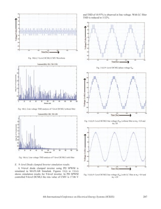
![Fig.5.Phase voltage of 3-level NPC-MLI Fig.6.Line voltage of 3-level NPC-MLI
Fig.7.CMV output using ZCM-SPWM Technique
Fig.5. shows phase voltage of three level neutral point
clamped inverter and Fig.6. presents line voltage of three level
neutral point clamped inverter using ZCM-SPWM
technique.CMV using ZCM-SPWM technique is shown in
Fig.7.
V. CONCLUSION
A three phase three level neutral point clamped inverter is
implemented in MATLAB/Simulink software using zero
common mode-sinusoidal pulse width modulation technique
for RL load. Simulation result shows that by using ZCM-
SPWM technique CMV is eliminated.
ACKNOWLEDGEMENT
Corresponding author Mohd Esa would like to extend his
gratitude and thanks to Mr.J.E.Muralidhar, Associate
Professor, EED, MJCET for his guidance, motivation, creative
ideas and support.
REFERENCES
[1] G.Bhuvaneswari and Nagaraju, “Multi-Level Inverters –
A Comparative Study,” IETE Journal of Research,
Vol.51, No. 2,pp.141-153, March-April 2005.
[2] Jay M.Erdman,R.J.Kerkman,D.W.Schlegel and
G.L.Skibinski , “Effect of PWM Inverters on AC Motor
Bearing currents and Shaft Voltages,” IEEE Transactions
on Industry Applications, Vol.32, No. 2 , pp.250- 259 ,
March/April 1996.
[3] Doyle Busse, Jay Eradman, R.J.Kerkman, Dave Schlegel
and Gary Skibinski , “System Electrical Parameters and
Their Effects on Bearing Currents,” IEEE Transactions on
Industry Applications ,Vol- 33, No.2, pp. 577-583,
March/April1997.
[4] S.Chen and T.A.Lipo, “Sources of Induction Motor
Bearing Currents Caused by PWM Inverters”, IEEE
Transactions on Energy Conversio, Vol. 11, No. 1, pp.
25-32, Mar. 1996.
[5] Doyle Busse, Jay Erdmann, R.J.Kerkman, Dave Schlegel
and Gary Skibinski, “Bearing Currents and Their
Relationship to PWM Drives” , IEEE Transactions on
Power Electronics, Vol. 12, N0. 2, pp.243-252, Mar.1997.
[6] S.Chen, T, A.Lipo and D.Fitzgerald, “Modeling of Motor
Bearing Currents in PWM Inverter Drives”, IEEE
Transactions on Industry Applications, Vol. 32, No.6, pp.
1365-1370, November/December, 1996.](https://image.slidesharecdn.com/ilovepdfmerged40-200326112403/85/Multilevel-Inverter-and-Multipliers-60-320.jpg)
![[7] H.Akagi and S.Tamura , “ A Passive EMI Filter for
Eliminating both Bearing Current and Ground Leakage
Current from an Inverter-Driven Motor, ” IEEE
Transactions on Power Electronics Vol.21,No.5 ,
pp.1459-1469 ,September 2006.
[8] R.S. Kanchan, P.N. Tekwani, M.R. Baiju, K. Gopakumar
and A. Pittet, “Three-level Inverter Configuration with
Common Mode Voltage Elimination for Induction Motor
Drive,” IEE Proc.- Electr. Power Appl., Vol. 152, No. 2,
pp.261-270, March 2005
[9] Alexander L. Julian, Giovanna Oriti, and Thomas A.
Lipo, “Elimination of Common-Mode Voltage in Three-
Phase Sinusoidal Power Converters,” IEEE Transactions
on Power Electronics Vol.14,No.5 , pp.982-989
,September 1999.
[10]M.M.Renge and H.M.Suryawanshi , “ Multilevel Inverter
to Reduce Common Mode Voltage in AC Motor Drives
Using SPWM Technique.” pp.21-27,Journal of Power
Electronics, Vol. 11, No. 1, January 2011
[11]M.M.Renge and H.M.Suryawanshi , “Five-Level Diode
Clamped Inverter to Eliminate Common Mode Voltage
and Reduce dv/dt in Medium Voltage Rating Induction
Motor Drives.”, IEEE Transactions on Power Electronics
,Vol.23 , No. 4 , pp.1598-1607,July,2008.
[12]Mohd Esa, Mohd Abdul Muqeem Nawaz and Syeda
Naheed, " Harmonic Analysis of Three level Flying
Capacitor Inverter ", International Research Journal of
Engineering and Technology (IRJET), vol. 04, no. 10, pp.
1687-1694, 2017.
[13]Mohd Esa and Mohd Abdul Muqeem Nawaz, "THD
analysis of SPWM & THPWM Controlled Three phase
Voltage Source Inverter", International Research Journal
of Engineering and Technology (IRJET), vol. 04, no. 10,
pp. 391-398, 2017.
[14]Mohd Esa and J.E.Muralidhar, "Investigation of
Common Mode Voltage in 5-level Diode Clamped MLI
using carrier based SPWM Techniques", International
Journal of Creative Research Thoughts (IJCRT), ISSN:
2320-2882, Volume.6, Issue 1, Page No pp.395-399,
February 2018
[15]M. Esa and J. E. Muralidhar, "Common Mode Voltage
reduction in Diode Clamped MLI using Phase Disposition
SPWM Technique," 2018 4th International Conference on
Electrical Energy Systems (ICEES), Chennai, India, 2018,
pp. 279-289. doi: 10.1109/ICEES.2018.8442411
[16]Mohd Esa and J.E.Muralidhar, "Common Mode
Voltage reduction in Diode Clamped MLI using
Alternative Phase Opposition Disposition SPWM
Technique", International Journal of Creative Research
Thoughts (IJCRT), ISSN: 2320-2882, Volume.6, Issue 2,
Page No pp.579-587, April-2018.
[17] Haoran Zhang,Annette von Jouanne,Shaoan Dai,Alan
k.Wallace and Fei Wang,”Multilevel Inverter Modulation
Schemes to Eliminate Common-Mode Voltages”,
IEEE Transactions on industry applications,vol.
36,no.6,November/December 2000.](https://image.slidesharecdn.com/ilovepdfmerged40-200326112403/85/Multilevel-Inverter-and-Multipliers-61-320.jpg)
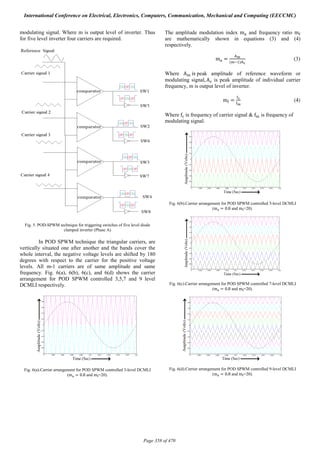
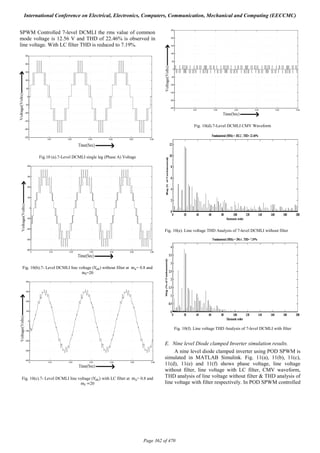
![www.ijcrt.org © 2017 IJCRT | National Conference Proceeding NTSET Feb 2018 | ISSN: 2320-2882
National Conference On Trends In Science, Engineering & Technology by Matrusri Engineering College & IJCRT
IJCRTNTSE081 International Journal of Creative Research Thoughts (IJCRT) www.ijcrt.org 395
INVESTIGATION OF COMMON MODE
VOLTAGE IN 5-LEVEL DIODE CLAMPED MLI
USING CARRIER BASED SPWM TECHNIQUES
Mohd Esa1
, J.E.Muralidhar2
1
M.E Student, Department of EEE, MJCET, Hyderabad
2
Associate Professor, Department of EEE, MJCET, Hyderabad
1
zmohdesa@gmail.com
Abstract: The main aim of this paper is to investigate the Common Mode Voltage (CMV) and Total Harmonic Distortion (THD) in
five level Diode Clamped Inverter using Carrier based SPWM techniques. The common mode voltage exists between neutral point of
star connected load and system ground. Various Carrier based SPWM techniques used to analyze CMV and THD in this paper are
Phase Disposition (PD) strategy, Phase Opposition Disposition (POD) strategy, Alternative Phase Opposition Disposition (APOD)
strategy, Carrier Overlap Phase Disposition (COPD) Strategy, Carrier Overlap Phase Opposition Disposition (COPOD) strategy and
Carrier Overlap Alternative Phase Opposition Disposition (COAPOD) strategy.RL load is connected to inverter circuit for analysis
purpose and Simulation is performed using MATLAB/Simulink Software.
IndexTerms: CMV, DCMLI, SPWM Techniques
I. INTRODUCTION
Common mode voltage is the voltage between neutral point of load and system ground [1] (or) voltage between star point of load
and D.C. midpoint (or) The common mode voltage (CMV) of the three-phase system is defined as the voltage potential difference
between the star point of the load network and the mid-point of the D.C. link capacitors[2].CMV always exists in PWM converters
regardless of number of levels and legs because of its switching operation. The high frequency and high amplitude CMV produced by
PWM inverter causes common mode current (CMC) via parasitic capacitor components between converter, loads, cables and ground
respectively. This CMC could be a source of consequent electromagnetic interference (EMI) noise & it may result in mal operation of
converter control system [3].CMV produced by PWM inverters induces shaft voltages on the rotor, when this shaft voltage exceeds
voltage limit of the lubricant in the bearings, results in large bearing currents, and this cause’s premature failure of bearings of
induction motor [4]. Multilevel inverter is one of the options to reduce this problem [5]. This paper is an attempt to investigate CMV
in 5-level Diode clamped Inverter using carrier based SPWM techniques.
Fig.2(a).Line voltage waveform for 5-level DCMLI
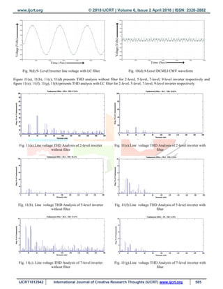
Fig.1.Five level DCMLI Fig.2(b).Phase voltage waveform for 5-level DCMLI](https://image.slidesharecdn.com/ilovepdfmerged40-200326112403/85/Multilevel-Inverter-and-Multipliers-62-320.jpg)
![www.ijcrt.org © 2017 IJCRT | National Conference Proceeding NTSET Feb 2018 | ISSN: 2320-2882
National Conference On Trends In Science, Engineering & Technology by Matrusri Engineering College & IJCRT
IJCRTNTSE081 International Journal of Creative Research Thoughts (IJCRT) www.ijcrt.org 396
II. CARRIER BASED SPWM TECHNIQUES
To control the output voltage of inverter different modulation strategies exists [6].The main modulation techniques are Sinusoidal
Pulse Width Modulation (SPWM) [7], Space Vector Pulse Width Modulation and Selective Harmonic Elimination Pulse Width
Modulation (SHEPWM).SPWM is simplest of all the above techniques. It was introduced by Schonung and Stemmler in 1964[8].In
carrier based SPWM technique for MLI, (m-1) triangular carriers are compared with one sinusoidal modulating signal. Where m is
output level of inverter. Thus for five level inverter four carriers are required [9]. The carrier based SPWM techniques are classified
according to non-overlapping carrier SPWM strategies and overlapping Carrier SPWM strategies.
Non overlapping carrier based SPWM Techniques are classified as follows
1. Phase Disposition (PD): All the carrier signals of same frequency, amplitude and phase, but having different DC offset
occupy levels one above the other are compared with a single sinusoidal modulating signal. All carriers above and below zero
reference are in same phase in PD SPWM technique [10].
2. Phase Opposition Disposition (POD): This method also contains carrier signals one above the other with same frequency,
amplitude but differ in phase, the carrier signals above reference zero voltage are in 180 degree out of phase with the carrier
signals below the zero reference voltage [10].
3. Alternative Phase Opposition Disposition (APOD): In APOD-SPWM technique the carrier signal of same amplitude are phase
displaced from each other by 180° from its neighboring carrier signals.
Overlapping carrier based SPWM Techniques are classified as follows
1. Carrier Overlapped Phase Disposition (COPD): Carriers in this technique overlapped each other such that overlapping carrier
distance between each carrier is half of the amplitude of carrier signal. In COPD all overlapped carriers are in same phase.
2. Carrier Overlapped Phase Opposition Disposition (COPOD): Carriers are divided equally into two groups according to
positive/negative average levels. In this type two groups are opposite in phase with each other while keeping in phase within
the group.
3. Carrier Overlapped Alternative Phase Opposition Disposition (COAPOD): Amplitude of carriers are overlapped with
neighbouring carriers phase shifted by 180 degrees from each other.
III. RESULTS & DISCUSSIONS
A 5-level diode clamped inverter using PD, POD, APOD, COPD, COPOD, COAPOD SPWM techniques is simulated in
MATLAB Simulink. Figure 3 and figure 4 shows simulation results for PD SPWM and POD SPWM Controlled 5-level inverter. In
PD SPWM controlled 5-level DCMLI the rms value of CMV is 40.33 V and THD of 39.30% is observed in phase voltage. In POD
SPWM controlled 5- level DCMLI the rms value of CMV is 18.76 and THD of 38.53% is observed in phase voltage.
(a) (b) (a) (b)
(c) (d) (c) (d)
Fig.3.PD-SPWM Controlled five level DCMLI (a) Carrier
arrangement (b) Phase Voltage (c) CMV waveform (d)
Harmonic Spectrum
Fig.4.POD-SPWM Controlled five level DCMLI (a)
Carrier arrangement (b) Phase Voltage (c) CMV
waveform (d) Harmonic Spectrum](https://image.slidesharecdn.com/ilovepdfmerged40-200326112403/85/Multilevel-Inverter-and-Multipliers-63-320.jpg)
![www.ijcrt.org © 2017 IJCRT | National Conference Proceeding NTSET Feb 2018 | ISSN: 2320-2882
National Conference On Trends In Science, Engineering & Technology by Matrusri Engineering College & IJCRT
IJCRTNTSE081 International Journal of Creative Research Thoughts (IJCRT) www.ijcrt.org 398
Table 2 shows CMV and %THD of 5-level Diode Clamped Inverter for 440V input DC voltage, 50Hz System frequency, 1000 Hz
switching frequency. Load resistance and Inductance of 100 Ohms and 50e-3 Henry are considered for analysis.
Table 2: CMV and %THD of 5-level DCMLI from different SPWM Methods
Method CMV(V) THD (%)
PD 40.33 39.30
POD 18.76 38.53
APOD 31.14 39.34
COPD 56.89 43.45
COPOD 31.46 39.56
COAPOD 21.35 37.57
Figure 9 shows variation of CMV and %THD for various SPWM Techniques. It can be clearly observed that POD SPWM controlled
5-level DCMLI has less CMV when compared to other SPWM techniques and THD is less in COAPOD controlled 5-level DCMLI.
Fig.9. Variation of CMV and %THD for various SPWM Techniques
IV. CONCLUSION
Five level Diode clamped inverter using Phase Disposition, Phase Opposition Disposition, Alternative Phase Opposition
Disposition, Carrier Overlapped Phase Disposition, Carrier Overlapped Phase Opposition Disposition and Carrier Overlapped
Alternative Phase Opposition Disposition SPWM techniques is simulated in MATLAB/Simulink Software. Simulation results
evidently shows that 5-level DCMLI using POD SPWM technique produces less CMV and COAPOD SPWM technique produces less
%THD in phase voltage. Shaft voltage and Bearing currents are also less in POD SPWM technique since they depends on CMV.Thus
POD SPWM technique is considered as best option for better operation of IM drives from above discussed techniques.
REFERENCES
[1] P. G. Shewane, S. Gaigowal, B. Rane, “Multicarrier Based SPWM Modulation for Diode Clamped MLI to reduce CMV and
THD”,Power, Automation and Communication [INPAC-2014], International Conference at Amravati on 6-8 OCT.2014, pp. 50-
54,DOI:10.1109/INPAC.2014.6981134, IEEE.
[2] E. Un and A. M. Hava, “A Near-State PWM Method With Reduced Switching Losses and Reduced Common-Mode Voltage for
Three-Phase Voltage Source Inverters,” Industry Applications, IEEE Transactions on, vol. 45, pp. 782-793, 2009.
[3] Min Zhang, “Investigation of Switching Schemes for Three-phase Four-Leg Voltage Source Inverters”, A thesis submitted for the
degree of Doctor of Philosophy June, 2013, School of Electrical and Electronic Engineering, Newcastle University
[4] Anuradha V.Jadhav and Mrs.P.V.Kapoor, “Reduction of common mode voltage using Multilevel Inverter”, Energy Efficient
Technologies for Sustainability [ICEETS], pp.586-590, 06 October 2016,DOI:10.1109/ICEETS.2016.7583822,IEEE.](https://image.slidesharecdn.com/ilovepdfmerged40-200326112403/85/Multilevel-Inverter-and-Multipliers-65-320.jpg)
![www.ijcrt.org © 2017 IJCRT | National Conference Proceeding NTSET Feb 2018 | ISSN: 2320-2882
National Conference On Trends In Science, Engineering & Technology by Matrusri Engineering College & IJCRT
IJCRTNTSE081 International Journal of Creative Research Thoughts (IJCRT) www.ijcrt.org 399
[5] M.M.Renge and H.M.Suryawanshi, “Multilevel Inverter to Reduce Common Mode Voltage in AC Motor Drives Using SPWM
Technique.”pp.21-27, Journal of Power Electronics, Vol. 11, No. 1, January 2011.
[6] Muhammad H. Rashid, “Power Electronics Hand book”, fourth edition, Butterworth-Heinemann, pp.399-400.
[7] Mohd Esa and Mohd Abdul Muqeem Nawaz, "THD analysis of SPWM & THPWM Controlled Three phase Voltage Source
Inverter", International Research Journal of Engineering and Technology (IRJET), vol. 04, no. 10, pp. 391-398, 2017.
[8] J.Y. Lee, and Y.Y. Sun, “A New SPWM Inverter with Minimum Filter Requirement’’, International Journal of Electronics, Vol.
64, No. 5, pp.815-826, 1988.
[9] McGrath, B.P.; Holmes, D.G.; "Multicarrier PWM strategies for multilevel inverters," Industrial Electronics, IEEE Transactions
on, vol.49, no.4, pp. 858- 867, Aug 2002 DOI:10.1109/TIE.2002.801073.
[10] Mohd Esa, Mohd Abdul Muqeem Nawaz and Syeda Naheed," Harmonic Analysis of Three level Flying Capacitor Inverter ",
International Research Journal of Engineering and Technology (IRJET), vol. 04, no. 10, pp. 1687- 1694, 2017.](https://image.slidesharecdn.com/ilovepdfmerged40-200326112403/85/Multilevel-Inverter-and-Multipliers-66-320.jpg)
![Mohd Esa al.Int. Journal of Engineering Research and Application www.ijera.com
ISSN: 2248-9622, Vol. 8, Issue 9 (Part –I) Sep 2018, pp. 36-41
www.ijera.com DOI: 10.9790/9622-0809013641 36 | P a g e
CMV analysis of 5-level Cascaded H-Bridge MLI with equal and
unequal DC sources using Variable Frequency SPWM Techniques
Mohd Esa*, Mohd Abdul Muqeem Nawaz** and Naheed***
*(Electrical Engineering Department, MJCET, Hyderabad-34
** (Electrical Engineering Department, MJCET, Hyderabad-34
*** (Electrical Engineering Department, MJCET, Hyderabad-34
Corresponding Author : Mohd Esa
ABSTRACT
This paper, investigates the Common Mode Voltage (CMV)between neutral point of the star connected RL load
and system ground.CMV also known as zero sequence voltage results in adverse effects like bearing currents,
shaft voltages and electromagnetic interference.CMV also causes premature failure of bearings of induction
motor and is necessary to reduce. In this paper, Variable Frequency Sinusoidal Pulse Width Modulation
(VFSPWM) techniques are used to investigate CMV in Cascaded H-Bridge Multilevel Inverter (CHB-MLI).
Comparison of 5-level CHB-MLI with equal and unequal DC sources in terms of CMV is also presented.
Simulation of circuit is carried out in MATLAB environment.
Keywords–CMV, CHB-MLI, VFSPWM
---------------------------------------------------------------------------------------------------------------------------------------
Date of Submission: 25-08-2018 Date of Acceptance: 08-09-2018
---------------------------------------------------------------------------------------------------------------------------------------
I. INTRODUCTION
Three phase inverters are normally used for
high power applications. The main function of the
inverter is to generate an ac voltage from a dc source
voltage [1].In recent years multi-level inverters are
used in high power and high voltage
applications.The multilevel inverter output voltage
has fewer harmonics compared to the conventional
inverter.
Multilevel inverters include an arrangement
of semiconductors devices and dc voltage sources to
generate a stepped output voltage waveform.
Multilevel inverters have drawn incredible interest in
power industry due to their advantages such as
higher efficiency, less common mode voltage, less
voltage stress on power switches, less dv/dt ratio, no
EMI problems and its suitability for high voltage and
high current applications [2].
The operations, power ratings, efficiency
&applications of multilevel inverter depends majorly
on its topology. The most commonly known
multilevel inverter topologies are Diode clamped
Multilevel Inverter [3], Flying capacitor Multilevel
Inverter [4], Cascaded-bridge Multilevel Inverter
[5].Fig.1 shows classification of multilevel inverters.
By combining these topologies with one another,
hybrid inverter topologies have also been developed.
In order to control MLI‟s, SPWM technique is used.
In SPWM technique, triangular shaped high
frequency carrier signal is compared with three
phase sinusoidal reference signal to generate gating
signals for triggering switches of inverter circuit.
Fig.1.Classification of Multilevel Inverters
The frequency of reference signal
determines the inverter output frequency &
amplitude of reference signal controls the
modulation index and in turn the rms output voltage
[6]. The classification of SPWM techniques is
shown in fig.2.In Multicarrier PWM technique for
MLI, (m-1) triangular carriers are compared with
sinusoidal modulating signal. Where m is output
level of inverter. Thus for five level inverter four
carriers are required.
RESEARCH ARTICLE OPEN ACCESS](https://image.slidesharecdn.com/ilovepdfmerged40-200326112403/85/Multilevel-Inverter-and-Multipliers-67-320.jpg)
![Mohd Esa al.Int. Journal of Engineering Research and Application www.ijera.com
ISSN: 2248-9622, Vol. 8, Issue 9 (Part –I) Sep 2018, pp. 36-41
www.ijera.com DOI: 10.9790/9622-0809013641 37 | P a g e
Fig.2.Classification of SPWM Techniques
The main drawback of conventional two
level inverter is higher common mode voltage which
can be reduced by using multilevel inverters. The
voltage between system ground and load neutral is
CMV.Equation (1) shows mathematical form of
CMV [7], [8].
CMV= (1)
Where are phase voltages
CMV= ∑
PWM inverter produces high frequency and high
amplitude CMV, which induces „shaft voltages‟ on
the rotor. Thus CMV is responsible for premature
failure of bearing of induction motor when supplied
from fast switching power components, so it is
necessary to reduce CMV by selecting specific
method [9].
In this paper, CMV is investigated in 5-level
CHB-MLI using VF-SPWM Techniques. Load of
R=100 Ohms and L=50e-3 Henry is considered.
II. CASCADED H-BRIDGE MLI
Cascaded H-Bridge multilevel inverter is
also known as multi-cell inverter. In this topology,
H-bridges with separate DC sources are connected in
series. For m level inverter number of cells required
is (m-1)/2.This topology requires less number of
components as there are no extra clamping diodes or
capacitors. The CHB-MLIs are best suited for
medium and high power applications, this is possible
because these MLIs has better harmonic spectrum at
low switching frequencies.
The source of bridges HB1, HB3 and HB5 is
Vdc1.The source of bridges HB4, HB6 and HB2 is
Vdc2.when magnitude of voltage source given to
HB1, HB3, HB5, HB4, HB6 and HB2 are equal then
Vdc1=Vdc2=Vdc.The principle of operation for Phase
A is shown in table 1.
Table 1: Switching states and output voltage for
leg-1 of three phase 5-level CHB-MLI with
equal voltage sources
When magnitude of voltage source given to
HB1, HB3, HB5is greater than HB4, HB6 and HB2
then Vdc1>Vdc2.When magnitude of voltage source
given to HB1, HB3, HB5 is lesser than HB4, HB6 and
HB2 then Vdc1<Vdc2. In such cases CHB-MLI is said
to be supplied from unequal DC source. Switching
pulses are given in similar manner as given in case
of CHB-MLI with equal sources. In this paper, both
CHB-MLI with equal and unequal DC sources are
compared in terms of CMV.
Fig.3.Three phase 5-level CHB-MLI](https://image.slidesharecdn.com/ilovepdfmerged40-200326112403/85/Multilevel-Inverter-and-Multipliers-68-320.jpg)
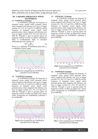
![Mohd Esa al.Int. Journal of Engineering Research and Application www.ijera.com
ISSN: 2248-9622, Vol. 8, Issue 9 (Part –I) Sep 2018, pp. 36-41
www.ijera.com DOI: 10.9790/9622-0809013641 40 | P a g e
Fig.11.VFSPWM-D controlled five level CHB-MLI
(a) phase voltage for CHB-MLI with equal DC
sources i.e. (b) CMV for CHB-MLI
with equal DC sources i.e. (c) phase
voltage for CHB-MLI with unequal DC sources i.e.
(d) CMV for CHB-MLI with unequal
DC sources i.e. (e) phase voltage for
CHB-MLI with unequal DC sources i.e.
(f) CMV for CHB-MLI with unequal DC sources i.e.
Table 2: CMV for VFSPWM controlled 5-level
CHB-MLI
V. CONCLUSION
A five level CHB-MLI has been simulated
in Matlab/Simulink software using VFSPWM-A,
VFSPWM-B, VFSPWM-C and VFSPWM-D
Techniques. CHB-MLI with equal and unequal DC
voltage source are compared and obtained CMV
values are tabulated. From table 2 it can be clearly
viewed that CMV is lesser in case of VFSPWM-D
technique when compared with other techniques
discussed. It can also be evident from table 2 that
CMV is lesser in case of CHB-MLI with equal
voltage sources when compared to CHB-MLI with
unequal voltage sources.
REFERENCES
Journal Papers:
[1]. Mohd Esa and Mohd Abdul Muqeem Nawaz,
"THD analysis of SPWM & THPWM
Controlled Three phase Voltage Source
Inverter", International Research Journal of
Engineering and Technology (IRJET), vol.
04, no. 10, pp. 391-398, 2017.
[2]. Mohd Esa and J.E.Muralidhar, "Common
Mode Voltage reduction in Diode Clamped
MLI using Alternative Phase Opposition
Disposition SPWM Technique", International
Journal of Creative Research Thoughts
(IJCRT), ISSN: 2320-2882, Volume.6, Issue
2, Page No pp.579-587, April-2018.
[3]. Mohd Esa and
J.E.Muralidhar, "Investigation of Common
Mode Voltage in 5-level Diode Clamped MLI
using carrier based SPWM Techniques",
International Journal of Creative Research
Thoughts (IJCRT), ISSN: 2320-2882,
Volume.6, Issue 1, Page No pp.395-399,
February 2018.
[4]. Mohd Esa, Mohd Abdul Muqeem Nawaz and
Syeda Naheed, "Harmonic Analysis of Three
level Flying Capacitor Inverter", International
Research Journal of Engineering and
Technology (IRJET), vol. 04, no. 10, pp.
1687-1694, 2017.
[5]. G. Prem Sunder, B. Shanthi, A. Lamehi
Nachiappan and S. P. Natrajan, “Performance
Analysis of modified CHB MLI using various
carrier modulation schemes”, IJESA, vol. 3,
no. 5, (2013), pp. 310-316.
[6]. B.P.Mcgrath and D.G Holmes “Multi carrier
PWM strategies for multilevel inverter” IEEE
Transaction on Industrial Electronics, Volume
49, Issue 4, Aug 2002, pp. 858-867
Proceedings Papers:
[7]. A. V. Jadhav, P. V. Kapoor and M. M. Renge,
"Reduction of common mode voltage in
motor drive application using multilevel
inverter," 2017 International Conference on
Energy, Communication, Data Analytics and
Soft Computing (ICECDS), Chennai, 2017,
pp.721-724.
[8]. A. V. Jadhav and P. V. Kapoor, "Reduction of
common mode voltage using multilevel
inverter," 2016 International Conference on
Energy Efficient Technologies for](https://image.slidesharecdn.com/ilovepdfmerged40-200326112403/85/Multilevel-Inverter-and-Multipliers-71-320.jpg)
![Mohd Esa al.Int. Journal of Engineering Research and Application www.ijera.com
ISSN: 2248-9622, Vol. 8, Issue 9 (Part –I) Sep 2018, pp. 36-41
www.ijera.com DOI: 10.9790/9622-0809013641 41 | P a g e
Sustainability (ICEETS),Nagercoil, 2016, pp.
586-590.doi: 10.1109/ICEETS.2016.7583822
[9]. M. Esa and J. E. Muralidhar, "Common Mode
Voltage reduction in Diode Clamped MLI
using Phase Disposition SPWM Technique,"
2018 4th International Conference on
Electrical Energy Systems (ICEES), Chennai,
India, 2018, pp. 279-289. doi:
10.1109/ICEES.2018.8442411
Mohd Esa "CMV analysis of 5-level Cascaded H-Bridge MLI with equal and unequal DC
sources using Variable frequency SPWM Techniques "International Journal of Engineering
Research and Applications (IJERA) , vol. 8, no.9, 2018, pp 36-41](https://image.slidesharecdn.com/ilovepdfmerged40-200326112403/85/Multilevel-Inverter-and-Multipliers-72-320.jpg)
![Study and Simulation of Liao’s Simplified Single-
Phase Five Level Inverter Topology
Mr.Mohd Esa, Mr.Mohd Abdul Muqeem Nawaz and Ms.Naheed
M.E. Students, Electrical Engineering Department.
M.J.C.E.T., Hyderabad, India
zmohdesa@gmail.com, muqeem4036@gmail.com, naheedsyed.9@gmail.com
Abstract— The objective of this paper is to study a simplified
single phase five level inverter topology with reduced number of
switches proposed by Liao. Single phase multilevel inverters are
the emerging power conversion technology used for micro-grid
applications. The main problem faced by multilevel inverters is
number of switches required which leads to higher switching
losses. In order to reduce conversion losses, the crucial thing is to
save costs and size by reducing the power semiconductor devices.
This paper witnesses the harmonic analysis of the Liao’s
simplified MLI topology using MATLAB Simulation software.
Keywords— DC/AC power conversion, Simplified MLI
I. INTRODUCTION
Multi-Level Inverters (MLI) have gained much attention for
past few years due to wide applications in electrical drives &
distributed power systems. Multilevel inverter performance is
high compared to the conventional two level inverters owing
to their advantages such as reduced harmonic distortion and
less electromagnetic interference [1]. MLI can generate near
sinusoidal voltages. MLI gives more sinusoidal form of ac
output from dc sources like solar cells, fuel cells & batteries.
Such ac output can be directly interfaced to the ac grid. MLI’s
can operate at both fundamental switching frequency and high
switching frequency PWM techniques [2].
Fig.1.Liao’s Simplified Five level Inverter Topology
The topologies of MLIs are classified into three types: the
flying capacitor inverter (FC-MLI) [3], the diode clamped
inverter (DC-MLI) and cascaded H-bridge inverter (CHB-
MLI).The main drawbacks of these MLI topologies are
increased number of switches, complex pulse width
modulation control & balancing of capacitor voltages. In order
to reduce conversion losses, size and cost of inverter circuit,
number of switches should be reduced. This reduction of
switches is obtained by Liao’s simplified MLI topology which
is discussed in this paper. Single phase simplified five level
inverter is shown in Fig.1.This topology consists of six power
switches two less than the Cascaded H Bridge MLI with eight
power switches which significantly reduces the power circuit
complexity. In this paper, Liao’s simplified MLI is simulated
and studied in terms of harmonics.
II. PRINCIPLE OF OPERATION
In the operation of Liao’s simplified single phase inverter
topology it is assumed that both input dc voltages are equal i.e.
. The switches operates
at high switching frequency whereas switches
operates at line frequency [4]. Table I shows switching
combinations that generate the required five output levels.
TABLE I: SWITCHING STATES AND MAGNITUDE OF OUTPUT
VOLTAGE
Switching States
2 OFF ON OFF ON OFF ON
OFF ON ON ON OFF OFF
ON ON OFF OFF OFF ON
0 ON ON ON OFF OFF OFF
0 OFF OFF OFF ON ON ON
- ON OFF OFF OFF ON ON
- OFF OFF ON ON ON OFF
-2 ON OFF ON OFF ON OFF
Steps to create the five level voltages using Liao’s Simplified
MLI are as follows
1. Maximum positive output voltage i.e. 2 : When
switches , and are ON, the voltage applied
to the RL load is 2 .
2. Half-level positive output voltage i.e. : This output
condition can be obtained by two different switching
combinations. One switching combination is such
that switches and are ON; the other is
such that switches and are ON. During](https://image.slidesharecdn.com/ilovepdfmerged40-200326112403/85/Multilevel-Inverter-and-Multipliers-73-320.jpg)
![this operating stage, the voltage applied to the RL
Load is .
3. Zero output voltage i.e. 0: This output condition can
be obtained by either of the two switching states.
Once the left or right switching leg is ON, the load
will be short-circuited and the voltage applied to the
RL load is zero.
Fig.2.Single Phase 5-level output waveform
4. Half-level negative output voltage i.e. - : This
output condition can be obtained by either of the two
different switching combinations. One switching
combination is such that switches , and are
ON; the other is such that switches , and
are ON.
5. Maximum negative output voltage i.e. - : When
the switches , and are ON, the voltage
applied to the RL load is -2 .
The switching loss of this topology is less when compared to
other conventional MLI’s and thus overall conversion
efficiency is improved.
III. MODULATION TECHNIQUE
Phase Disposition PWM switching scheme is easy to
implement in both analogue and digital circuit [5]. It is most
popular in Industrial applications. The modulation technique
used to trigger switches of Liao’s simplified single phase five
level inverter uses two reference waveforms and two carrier
waveforms. Carrier signal frequency is very high when
compared to reference signal. Modulation logic for Liao’s
simplified single phase five level inverter is shown in Fig.3.
Fig.4 and Fig.5(a)-5(f). shows carrier/reference signals
arrangement and pulses to switches of Liao’s simplified single
phase five level inverter respectively. The phase disposition
PWM control scheme is used to generate switching signals
and to produce five output-voltage levels i.e.
0, .
Two comparators are used in this scheme with identical
carrier signals to provide high-frequency switching signals for
switches The pulses generated by
comparing reference signal-1 and carrier signal-1 is provided
to switches and and the pulses generated by comparing
reference signal-2 and carrier signal-2 is provided to switches
and .A separate pulse generator is used to provide
pulses at line frequency to switches and . The quality
of output voltage of inverter strongly related to Total
Harmonic Distortion (THD) .THD is the measure of effective
value of harmonic components of a distorted waveform [6]. In
this paper, using PD-PWM technique harmonic analysis of
Liao’s simplified single-phase five level inverter topology is
carried.
Fig.3.Modulation logic for Liao’s simplified single phase five
level inverter
Fig.4. Carrier/reference signals arrangement
Fig.5(a)-5(f).Pulses to switches of Liao’s simplified single
phase five level inverter](https://image.slidesharecdn.com/ilovepdfmerged40-200326112403/85/Multilevel-Inverter-and-Multipliers-74-320.jpg)
![TABLE II: COMPARISON OF LIAO’S SIMPLIFIED INVERTER WITH
OTHER TOPOLOGIES
Components
Single Phase Five Level
Inverter Topology
DC-
MLI
FC-
MLI
CHB-
MLI
Liao’s
MLI
DC bus capacitors 4 4 2 2
Main switches 8 8 8 6
Main diodes 8 8 8 6
Clamping diodes 12 0 0 0
Flying capacitors 0 6 0 0
Total component count 32 26 18 14
V. CONCLUSION
Liao’s simplified single phase 5-level inverter topology is
studied and simulated in MATLAB/Simulink software.
Harmonic analysis is carried out and simulation result clearly
shows that current THD is 1.88% and Voltage THD is
26.06%. Comparison of Liao’s MLI with DC-MLI, FC-MLI
and CHB-MLI is presented in terms of components required.
Table II shows that Liao’s simplified MLI produces a
significant reduction in the number of power devices required
to implement multilevel output.
References
[1] Mohd Esa, Mohd Abdul Muqeem Nawaz and Syeda Naheed, "
Harmonic Analysis of Three level Flying Capacitor Inverter ",
International Research Journal of Engineering and Technology (IRJET),
vol. 04, no. 10, pp. 1687-1694, 2017.
[2] Mohd Esa and J.E.Muralidhar, "Investigation of Common Mode
Voltage in 5-level Diode Clamped MLI using carrier based SPWM
Techniques", International Journal of Creative Research Thoughts
(IJCRT), ISSN: 2320-2882, Volume.6, Issue 1, Page No pp.395-399,
February 2018.
[3] Mohd Esa and J.E.Muralidhar,"Common Mode Voltage reduction in
Diode Clamped MLI using Alternative Phase Opposition Disposition
SPWM Technique", International Journal of Creative Research
Thoughts (IJCRT), ISSN: 2320-2882, Volume.6, Issue 2, Page No
pp.579-587, April-2018.
[4] Y. H. Liao and C. M. Lai, " Newly-Constructed Simplified Single-Phase
Multistring Multilevel Inverter Topology for Distributed Energy
Resources ",IEEE Transactions on Power Electronics, vol. 26, no. 9, pp.
2386-2392, Sept., 2011.
[5] M. Esa and J. E. Muralidhar, "Common Mode Voltage reduction in
Diode Clamped MLI using Phase Disposition SPWM Technique," 2018
4th International Conference on Electrical Energy Systems (ICEES),
Chennai, India, 2018, pp. 279-289. doi: 10.1109/ICEES.2018.8442411
[6] Mohd Esa and Mohd Abdul Muqeem Nawaz, "THD analysis of SPWM
& THPWM Controlled Three phase Voltage Source Inverter",
International Research Journal of Engineering and Technology (IRJET),
vol. 04, no. 10, pp. 391-398, 2017.](https://image.slidesharecdn.com/ilovepdfmerged40-200326112403/85/Multilevel-Inverter-and-Multipliers-76-320.jpg)
![Study and Simulation of Seven Level - Ten Switch
Inverter Topology
Mohd Esa1
and Syed Abdul Moiz1
1
Electrical Engineering Department, Muffakham Jah College of Engineering and
Technology, Banjarahills, Hyderabad, India
{zmohdesa,moizsyed206}@gmail.com
Abstract. Compared to conventional two-level inverter, multilevel inverter
performance is high because of their reduced harmonic distortion, less
electromagnetic interference, reduced common mode voltage and higher dc link
voltages. However complex pulse width modulation control, balancing of
capacitor voltages & increased number of switches are main drawbacks of
multilevel inverter.This paper focuses on study and simulation of single phase
seven level inverter topology using only ten switches. This paper also presents
two different control techniques for seven level-ten switch inverter topology.R-
load is connected to inverter and simulation is performed using
MATLAB/Simulink Software.
Keywords: Multilevel Inverter, Power electronics, SPWM Techniques.
1 Introduction
In recent research, there has been an extensive increase in interest to multilevel power
conversion. The introduction of new inverter topologies & unique modulation
techniques was involved in recent research studies. However, the most commonly
used multi-level inverter topologies are multi-cell inverter [1], diode clamped inverter
[2]-[5] and capacitor clamped inverter [6]. Some applications for these inverters
include industrial drives, flexible ac transmission systems [7], traction applications in
the transport industry and grid integration of non-conventional energy sources.
The seven level-ten switch topology is a symmetrical topology since the values of
all voltage sources are the same. However, there are several asymmetrical topologies
that need voltage sources of different values. This asymmetry results in the need of dc
voltage sources having a specific relation between them and also the difference in
rating of the semiconductor switches. This paper, presents study and simulation of a
new multilevel inverter topology named reversing voltage (RV) [8]. This topology
requires less number of components compared to conventional topologies. It is also
more efficient since the inverter has a component which operates the switching power
devices at line frequency. Therefore, there is no need for all switches to work in high
frequency which leads to simpler and more reliable control of the inverter. Two
different control techniques are used in this paper to drive the inverter .The simulation
results of the seven level-ten switch inverter topology are presented.
International Journal of Research
Volume VIII, Issue I, January/2019
ISSN NO:2236-6124
Page No:798](https://image.slidesharecdn.com/ilovepdfmerged40-200326112403/85/Multilevel-Inverter-and-Multipliers-77-320.jpg)
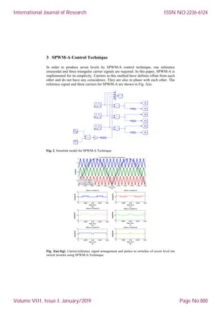
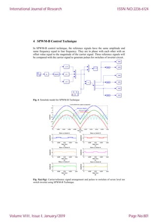
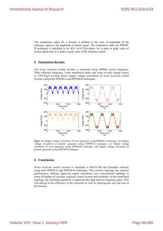
![RTL Verification and FPGA Implementation of 4x4
Vedic Multiplier
Mohd Esa , Konasagar Achyut and Chandrajeet Singh
Abstract. The objective of this paper is to study 4x4 Vedic multiplier.
Multiplication is an important fundamental function in arithmetic operations.
Vedic multiplier using Urdhva-Tiryagbyam sutra is predominant in
performance evaluation of parameters such as power, area & delay. This paper
presents design, verification and FPGA implementation of Vedic multiplier.
Verification is carried out in Questa Sim 10.4e using System Verilog HVL and
design is carried out in Xilinx ISE Design Suite 14.7 using Verilog HDL
environment.
Keywords: Vedic Multiplier, HVL, HDL, RTL, FPGA.
1 Introduction
inary number system uses only zero‟s and one‟s. Just like decimal system,
binary possesses every arithmetic operation. A binary multiplier is any such
electronic circuit used in digital electronics to multiply two binary numbers
[1]. Unlike the decimal base ten, binary multiplication is done in binary base two. The
concept of Vedic multiplier has been acquired from the Vedic mathematics in which
there are several methods to operate with the number systems.Urdhva-Triyagbhyam
sutra is one among those Vedic methods which helps to follow general formula
applicable to all cases in multiplication. The meaning of Urdhva-Triyagbhyam is
vertically and crosswise.
This paper presents the design and verification of 4x4 bit Vedic multiplier
using HDL and HVL respectively, which helps us to justify that design is working
without any bugs or errors. This paper also presents implementation of Vedic
multiplier in Field Programming Gate Array.FPGAs are semiconductor devices that
are based around a matrix of configurable logic blocks connected via programmable
interconnects. FPGAs can be reprogrammed to desired application or functionality
requirements after manufacturing.
2 Ripple Carry Adder
As the name of the circuit itself represents that the carry is rippled to a
succeeding part. The combination of full adders whose carry output is propagated as a
B
Parishodh Journal
Volume IX , Issue III , March/2020
ISSN NO:2347-6648
Page No:772](https://image.slidesharecdn.com/ilovepdfmerged40-200326112403/85/Multilevel-Inverter-and-Multipliers-83-320.jpg)
![carry input to the succeeding full adder is called as a Ripple Carry Adder. The
addition of two binary numbers in parallel implies that all the bits of addend and
augend are available for computation at the same time [2].
Fig.1. Ripple Carry Adder logic circuit
Table 1.Ripple Carry Adder truth table
In this work, three ripple carry adders are used in which the first bits from addend and
augend binary numbers are computed by half adders and rest with full adders to form
a complete ripple addition. The truth table for various possible combinations of ripple
carry adder is shown table 1.
3 Urdhva Triyagbhyam Sutra
Mathematics is mother of all sciences, it is full of mysteries and magic.
Ancient Indians were able to understand these mysteries and developed simple keys
to solve them. The ancient system of Vedic maths was introduced by Swami Bharati
Krishna Tirthaji. His work includes various methods of calculations and this in turn
Indians named it as Vedic mathematics [3].
This paper presents multiplication operation done over two 4-bit binary
numbers through the Urdhva-Triyagbhyam technique. As usual the multiplication has
a multiplier and a multiplicand, but the method of multiplication is done by
multiplying first two bits of multiplicand and multiplier followed by cross
multiplication of side numbers of multiplicand with numbers in multiplier, finally the
last digits are multiplied parallelly to complete the multiplication process. This
method can be observed as shown in the fig.2 for two bit binary numbers. To perform
this in digital logic the block diagram of two bit Vedic multiplier is shown in fig.3.
Parishodh Journal
Volume IX , Issue III , March/2020
ISSN NO:2347-6648
Page No:773](https://image.slidesharecdn.com/ilovepdfmerged40-200326112403/85/Multilevel-Inverter-and-Multipliers-84-320.jpg)
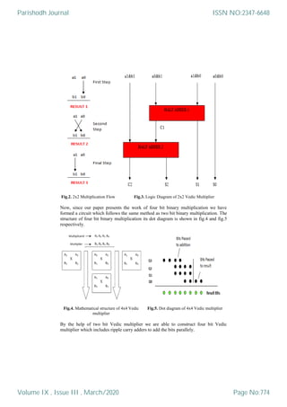
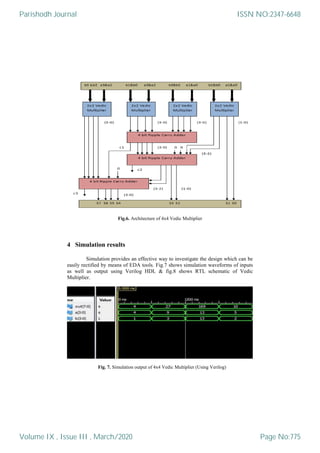
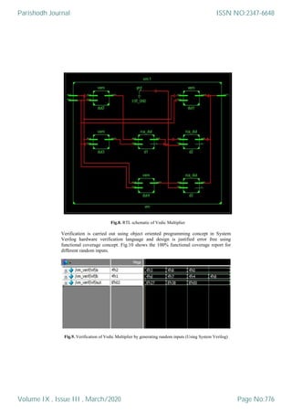
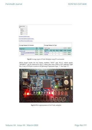
![Design and Verification of 4 X 4 Wallace Tree
Multiplier
Mohd Esa and Konasagar Achyut
Abstract. The aim of this paper is to study 4x4 Wallace tree multiplier. In high
performance processing units & computing systems, multiplication of two
binary numbers is primitive and most frequently used arithmetic operation.
Wallace tree multiplier is area efficient & high speed multiplier. This paper
presents design and verification of Wallace tree multiplier. Design is carried out
in Xilinx ISE Design Suite 14.7 using Verilog HDL and verification is carried
out in Questa Sim 10.4e using System Verilog HVL environment.
Keywords: Wallace Multiplier, HVL, HDL, RTL.
1 Introduction
echnology is growing rapidly and being developed since years, today human is
totally dependent on technology over the entire range of things. All these
things which are manufactured and brought to market has its own
disadvantages & advantages with its scaled reliability, product designers keep the
three metaphoric terms constantly in the vision and improve them year by year: Area,
Speed and Power. This paper is the entirety of the multiplication done in digital
electronics by means of binary system.
Binary arithmetic consists of subtraction, multiplication, addition & division.
This paper is all about designing and verifying the functionality of Wallace tree
multiplier. A binary number system has only 1 and 0 as digits. Multipliers play a
necessary role in today’s digital signal processing and various other applications.
Wallace tree multiplier is structured hardware implementation of digital circuit which
multiplies two integers as formulated by Chris Wallace, an Australian computer
scientist in 1964. The prominent components used in this multiplier are:
(a) Full Adder:
Combinational logic is a concept in which two or more input states describe one or
more output states. Design of a full adder [1], First, we must create a truth table
showing the various input and output values for all the possible cases. Fig.1 shows the
logical diagram having three inputs A, B, Cin and two outputs, Sum and Cout. There
are eight possible cases for three inputs, and for each case the desired output values
are listed. For example the case A = T, B = F and Cin = T. The full adder must add
these three bits to produce a sum of F and a carry (Cout) of T [2]. Two half adders and
T
The International journal of analytical and experimental modal analysis
Volume XI, Issue X, October/2019
ISSN NO: 0886-9367
Page No:655](https://image.slidesharecdn.com/ilovepdfmerged40-200326112403/85/Multilevel-Inverter-and-Multipliers-90-320.jpg)
![OR gate can be combined to make a full adder as shown in fig.1. Table 1 shows that
there are four cases where sum is to be a T and four cases where sum is F [3].
Table 1.Full adder truth table
Input Output
A B Cin Sum Cout
F F F F F
F T F T F
T F F T F
T T F F T
F F T T F
F T T F T
T F T F T
T T T T T
Fig. 1. Logic diagram of full adder
(b) Half Adder:
Full adder operates on three inputs to produce a sum and a carry output. In some
cases, a circuit is needed that will perform addition of only two input bits, to produce
a sum and a carry output.
Table 2.Half adder truth table
Input Output
A B Sum Cout
F F F F
T T F T
T F T F
F T T F Fig. 2. Logic diagram of half adder
An example would be the addition of LSB position of two binary numbers where
there is no carry input to be added. A special logic circuit can be designed to take two
input bits, A & B, and to produce sum and carry (Cout) outputs. This circuit is called
half adder whose task is similar to that of a full adder except that it functions on only
two bits. The simplest half adder design includes an XOR gate for sum and an AND
gate for Cout. The input variables of half adder are called augend and addend bits.
With the emergence of Large Scale Integration, engineers are able to put
thousands of gates on a single chip. At this instance design process started getting
very difficult and engineers sensed the need to automate the process. Electronic
Design Automation (EDA) techniques began to emerge. Because of the complexity of
the circuits it wasn’t possible to verify these circuits on breadboard and analyse it
The International journal of analytical and experimental modal analysis
Volume XI, Issue X, October/2019
ISSN NO: 0886-9367
Page No:656](https://image.slidesharecdn.com/ilovepdfmerged40-200326112403/85/Multilevel-Inverter-and-Multipliers-91-320.jpg)
![accurately. Thus HDLs came into existence [4]. The Verilog Hardware description
Language (HDL) became the most extensively used language for hardware
description. Verification is intended to be fundamentally different activity than
design. This splitting has led to development of narrow focused language for
verification.
2 Wallace Tree Multiplier
The initial step is the formation of partial products by multiplying each bit from the
multiplier to same bit position of multiplicand. Secondly, groups of three adjacent
rows are collected. Each group of three rows is reduced by using half adders and full
adders.
Fig. 3. Operation of 4x4 Wallace Tree Multiplier
Half adders are used in each column where there are two bits whereas full adders are
used in each column where there are three bits, any single bit in column is passed to
next stage in the same column without any operation. This reduction procedure is
repeated in each successive stage until only two rows remain. In the final stage, the
remaining two rows are added. After completing all the three stages we get 8 bit of
output as shown in fig.5.
Fig.4.Block diagram of Wallace Tree Multiplier
The International journal of analytical and experimental modal analysis
Volume XI, Issue X, October/2019
ISSN NO: 0886-9367
Page No:657](https://image.slidesharecdn.com/ilovepdfmerged40-200326112403/85/Multilevel-Inverter-and-Multipliers-92-320.jpg)
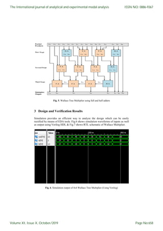
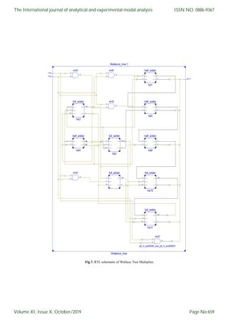
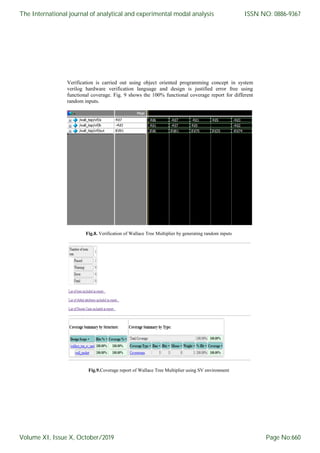


The document details the educational background and research interests of an author named Mohd Esa, who completed his M.E. in Power Electronics Systems and has published 12 research papers. It focuses on a study comparing two modulation techniques for three-phase inverters: Sinusoidal Pulse Width Modulation (SPWM) and Third Harmonic Pulse Width Modulation (THPWM), analyzing their effectiveness in reducing total harmonic distortion (THD). The results demonstrate that THPWM generally performs better than SPWM across various carrier frequencies.