This paper presents a new approach to minimizing common mode voltage in cascaded multilevel inverters using level shifted discontinuous pulse-width modulation (PWM) algorithms. The proposed method combines conventional discontinuous PWM with zero sequence signal injections to enhance performance and reduce switching losses while achieving less harmonic distortion. Experimental validation demonstrates the effectiveness of this technique for induction motor drives, highlighting improved efficiency and reduced common-mode voltage.
![International Journal of Power Electronics and Drive System (IJPEDS)
Vol. 9, No. 2, June 2018, pp. 504~518
ISSN: 2088-8694, DOI: 10.11591/ijpeds.v9.i2.pp504-518 504
Journal homepage: http://iaescore.com/journals/index.php/IJPEDS
Level Shifted Discontinuous PWM Algorithms to Minimize
Common Mode Voltage for Cascaded Multilevel Inverter Fed
Induction Motor Drive
M. Nayeemuddin1
, T. Bramhananda Reddy2
, M. Vijaya Kumar3
1
Department of Electrical Engineering, JNTUA, Anathapuramu, India
2
Department of Electrical Engineering, G.Pulla Reddy Engineering College, Kurnool, India
3
Department of Electrical Engineering, JNTUA, Anathapuramu, India
Article Info ABSTRACT
Article history:
Received Jan 12, 2018
Revised Apr 10, 2018
Accepted Apr 24, 2018
This paper presents combinations of level shifted pulse-width modulation
algorithm with conventional discontinuous pulse-width modulation methods
for cascaded multilevel inverters. In the proposed DPWM a zero sequence
signal is injected in sinusoidal reference signal to generate various
modulators with easier implementation. The analysis four various control
strategies namely Common Carrier (CC), Inverted Carrier (IC), Phase Shifted
(PS) and Inverted Phase Shift (IPS) for cascaded multilevel inverter fed
induction motor drive has been illustrated. To validate the proposed work
experimental tests has been carried out using dSPACE controller.
Experimental study proves that using proposed algorithms reduction in
common-mode voltage with fewer harmonics along with reduced switching
loss for a cascaded multilevel inverter fed motor drive has been achieved
Keyword:
Cascaded multi level inverter
Multicarrier PWM
Common mode voltage (CMV)
DPWM
Total harmonics distortion Copyright © 2018 Institute of Advanced Engineering and Science.
All rights reserved.
Corresponding Author:
M. Nayeemuddin,
Departement of Electrical Engineering,
Research Scholar, JNTUA, Anantapuramu, India
Email: nayeemgprec@gmail.com
1. INTRODUCTION
In recent years, multilevel inverters have been intensively developed for industrial power converters
and some of interesting advantages of multilevel inverters such as low distortion in output voltage with
relative less common mode voltage, low harmonic and electromagnetic interference (EMI), attracted
researcher attentions [1-4]. Multilevel Inverters are used in many applications such as uninterruptible power
supply (UPS), Medium voltage Industrial (induction motor) drives, ship propulsion Induction heating, high
voltage direct current (HVDC) power transmission, grid connected photovoltaic system, railway locomotives,
active filters, wind Energy System, and applications of power system for example flexible AC transmission
(FACTS). As the number of levels increases the output of the voltage is very close to sinusoidal signal
reduces harmonic distortion.
Their main topologies such as: diode-clamped type, cascaded type and capacitor clamped type are
commonly used as shown in Figure 1. Three PWM techniques such as selective harmonic elimination PWM
(SHEPWM), carrier-based PWM (CPWM), and space vector PWM (SVPWM) , have been favorably used in
practice. Because of having a small number of switching, the selective harmonic elimination PWM method
shows be advantageous for high power applications. Two remaining PWM techniques are commonly used in
various fields because of their excellent PWM qualities. The DPWM methods of two-level inverters have
been studied for many years, and they are introduced as an approach to reduce the switching loss [5-6].
DPWM methods can be realized using space vector PWM approach by eliminating one from the redundant
zero vectors in the switching state sequence ; or carrier-based PWM ones by adding offset to make some leg-](https://image.slidesharecdn.com/0410apr1812jan1810536-14679-1-ededitlelli-210611040025/75/Level-Shifted-Discontinuous-PWM-Algorithms-to-Minimize-Common-Mode-Voltage-for-Cascaded-Multilevel-Inverter-Fed-Induction-Motor-Drive-1-2048.jpg)
![Int J Pow Elec & Dri Syst ISSN: 2088-8694
Level shifted Discontinuous PWM Algorithms to minimize common mode voltage … (M. Nayeemuddin)
505
voltage attain one of two dc-rail levels [7-10]. Some studies were concentrated on the analyzing the impacts
of DPWM waveforms on the current ripple.
Three level inverters continue to attract the attention of researchers ever since introduced by
Nabae,A. et.al. [11]. Though simple and elegant, the neutral-clamped circuit topology suggested in [11], has
a few disadvantages. The neutral point fluctuation is a commonly encountered problem in this configuration,
as the capacitors connected to the DC-bus carry load currents. Also, there is an ambiguity regarding the
voltage rating of the semi-conductor devices, which are connected to the neutral point. This calls for a
conservative selection of these devices for reliable operation, enhancing the cost.
In this paper, a new circuit configuration for a 3-level inverter as shown in figure1 has been
proposed. In this circuit configuration, 3-level inversion is realized by connecting two 2-level inverters in
cascade as shown in Figure 1. The DC-link capacitors in this circuit do not carry the load currents and hence
the voltage fluctuations in the neutral point are absent. However, the power semi-conductor switches in one
bank (three in number) in one of the inverters in this circuit have to be rated for the full DC-link voltage.Each
inverter is powered with an isolated DC-power supply, with a voltage of Vdc/2 in Figure 1. The symbols
Va1o, Vb1o, Vc1o respectively denote the output voltages of inverter-1 with respect to the point 'O' in Figure 1.
Similarly, the symbols Va2o, Vb2o, Vc2o respectively denote the pole voltages of inverter-2 with respect to the
point 'O' in Figure 1.
S11
c1
b1
a1
Vdc/2 Induction
Motor
Drive
Vdc/2
o
S13 S15
S14 S16 S12
S21 S23 S25
S24 S26 S22
c2
b2
a2
Figure 1. Proposed three-level cascaded inverter configuration
The pole voltage of any phase in inverter-2 attains a voltage of Vdc, under the following conditions:
a) The top switch of that leg in inverter-2 is turned on.
b) The top switch of the corresponding leg in inverter-1 is turned on.
Similarly the pole voltage of any phase for inverter-2 attains a voltage of Vdc/2, under the following
conditions:
a) The top switch of that leg in inverter-2 is turned on.
b) The bottom switch of the corresponding leg in inverter-1 is turned on.
Thus, the DC-input points of individual phases of inverter-2 may be connected to a DC-link voltage
of either Vdc or Vdc/2 by turning on the top switch or the bottom switch of the corresponding phase leg in
inverter-1.
Additionally, the pole voltage of a given phase in inverter-2 attains a voltage of zero, if the bottom
switch of the corresponding leg in inverter-2 is turned on. In this case, the DC-input point of that phase for
inverter-2 is floating as the top and bottom switches are switched complimentarily in any leg in a 2-level
inverter. Thus, the pole voltage of a given phase for inverter-2 is capable of assuming one of the three
possible values 0, Vdc/2 and Vdc which is the characteristic of a three level inverter.The mathematical
expression for the common mode potential can be derived from the inverter pole voltages as
3
2
2
2 o
c
o
b
o
a
com
V
V
V
V
](https://image.slidesharecdn.com/0410apr1812jan1810536-14679-1-ededitlelli-210611040025/75/Level-Shifted-Discontinuous-PWM-Algorithms-to-Minimize-Common-Mode-Voltage-for-Cascaded-Multilevel-Inverter-Fed-Induction-Motor-Drive-2-2048.jpg)
![ ISSN: 2088-8694
Int J Pow Elec & Dri Syst, Vol. 9, No. 2, June 2018 : 504 – 518
506
Table 1. Pole Voltage of Inverter-2
Switches turn on Inverter-I Switches turn on Inverter-2 pole voltage of Inverter-2
S14 or S16 or S12 S21 or S23 or S25 Vdc
S14 or S16 or S12 S21 or S23 or S25 Vdc/2
S11 or S13 or S15 S22 or S24 or S26 0
S11 or S13 or S15 S22 or S24 or S26 0
2. SIMPLIFIED DISCONTINOUS PWM ALGORITHM
Conventional SVPWM technique can be implementation in digital approach or in carrier based
modulation approach. In CSVPWM algorithm, the desired reference voltage vector is generated by time
averaging the suitable discrete voltage vectors in every sub cycle or sampling time period Ts. For a given
reference voltage vector and Ts, the duration T1, T2 and TZ are unique. The expressions for the various
active state time durations and zero states time duration in the first sector can be given in [3]
s
ref
T
V
T
)
3
sin(
3
sin
1
(1)
s
ref
T
V
T
)
3
sin(
3
sin
1
(2)
2
1 T
T
T
T s
Z
(3)
The calculation of switching times requires angle and sector information which increases
complexity of the algorithm. Hence to reduce complexity involved in conventional SVPWM, simplified
scalar PWM algorithm has been proposed which does not require angle and sector information.
Consider three reference signals expressed as
)
3
/
)
1
-
(
2
-
(
*
j
t
w
Sin
V
V e
p
i
Where i=a,b,c and j=1,2,3 ( i = j )
(4)
It is recognized and proposed that an addition of a zero sequence signal to each of the reference
modulator makes it possible to utilize the DC bus voltage 15.5% more as compared with conventional
SPWM method. It means that it is possible to increase the fundamental output voltage of the inverter by
15.5%. On the other hand the use of zero sequence signal [12-13] not only increases the DC bus utilization
by 15.5% but also reduces the switching loss of the inverter, it means that number of on and off of the
inverter switch is reduced by 33% by clamping each of the pole voltage to either positive bus or negative bus
for a period of 120o
.
The proposed simplified discontinuous algorithm uses the concept of injected zero sequence signal
[12-13], different modulators can generated by adding the zero sequence component to the three phase
reference sinusoidal signal, different zero sequence components thus leads to different modulating signals
with different properties.A generalized expression that generates the zero sequence components V0 as a
function of VM, Vm and Z0 is given by [14]
]
*
)
1
(
*
)
*
2
1
[( 0
0 m
o
M
o V
Z
V
Z
Z
V
(5)
Where
7
0
7
0
T
T
T
Z
(6)](https://image.slidesharecdn.com/0410apr1812jan1810536-14679-1-ededitlelli-210611040025/75/Level-Shifted-Discontinuous-PWM-Algorithms-to-Minimize-Common-Mode-Voltage-for-Cascaded-Multilevel-Inverter-Fed-Induction-Motor-Drive-3-2048.jpg)
![Int J Pow Elec & Dri Syst ISSN: 2088-8694
Level shifted Discontinuous PWM Algorithms to minimize common mode voltage … (M. Nayeemuddin)
507
Zero Sequence
Component (Vo)
Level Shifting Signal.
Level Shifting Signal
INVERTER-2
INVERTER-1
Vb
Vc
Va
Figure 2. Block diagram illustrating scalar PWM for cascaded three level inverter configuration
By using the zero sequence component various PWM Modulators can be generated, can be
expressed in terms of V0 and reference signal as
o
V
i
V
i
V
* (7)
T0+T7 = Tz gives the total freewheeling time (Zero state time) of the inverter, VM and Vm are the
maximum and minimum values of the three phase reference signal (Vi).Moreover, by utilizing the concept of
unequal division of zero state time, various PWM algorithms can be generated. In the proposed simplified
DPWM algorithm, by varying the zero sequence component partition parameter Zo between 0 and 1, various
PWM algorithms can be generated.
Table 2: Generation of CPWM and DPWM algorithms
S
No.
PWM algorithm Zero sequence Component o
V value
1 CSVPWM Vo = -(VM+Vm)/2
2 DPWM1
If |Vm|> VM Vo = -(1+Vm)
If |Vm|< VM Vo = (1-VM)
When Z0=0.5, from equation (7) describes the equal division of zero state time, i.e. T0=T7 which
results in the conventional space vector PWM algorithm, and the corresponding zero sequence component is
equal to average of VM & Vm , V0= - (VM+Vm )/2.Among various Continuous PWM possibilities, Z0=0.5 is
the best choice which have been concluded in the literature[15]. In case DPWM, change of Z0 from 1 to 0
coincides with middle of the reference signal, the resultant modulating signal is known as DPWM1 which
clamps at any fundamental time instant one of the pole is connected to negative bus for a period of 1200
while the other two are modulating.
Figure 3. Showing DPMW1 Moulator
0 60 120 180 240 300 360
-1
0
1
(a)
0 60 120 180 240 300
-1
0
1
(b)
0 60 120 180 240 300 360
-1
0
1
(c)
0 60 120 180 240 300
-1
0
1
(d)
0 60 120 180 240 300 360
-1
0
1
(e)
0 60 120 180 240 30
-1
0
1
(f)
0 60 120 180 240 300 360
-1
0
1
0 60 120 180 240 30
-1
0
1
Zo=0
Zo=0.5
Zo=1
Zo=0
Zo=1](https://image.slidesharecdn.com/0410apr1812jan1810536-14679-1-ededitlelli-210611040025/75/Level-Shifted-Discontinuous-PWM-Algorithms-to-Minimize-Common-Mode-Voltage-for-Cascaded-Multilevel-Inverter-Fed-Induction-Motor-Drive-4-2048.jpg)
![ ISSN: 2088-8694
Int J Pow Elec & Dri Syst, Vol. 9, No. 2, June 2018 : 504 – 518
508
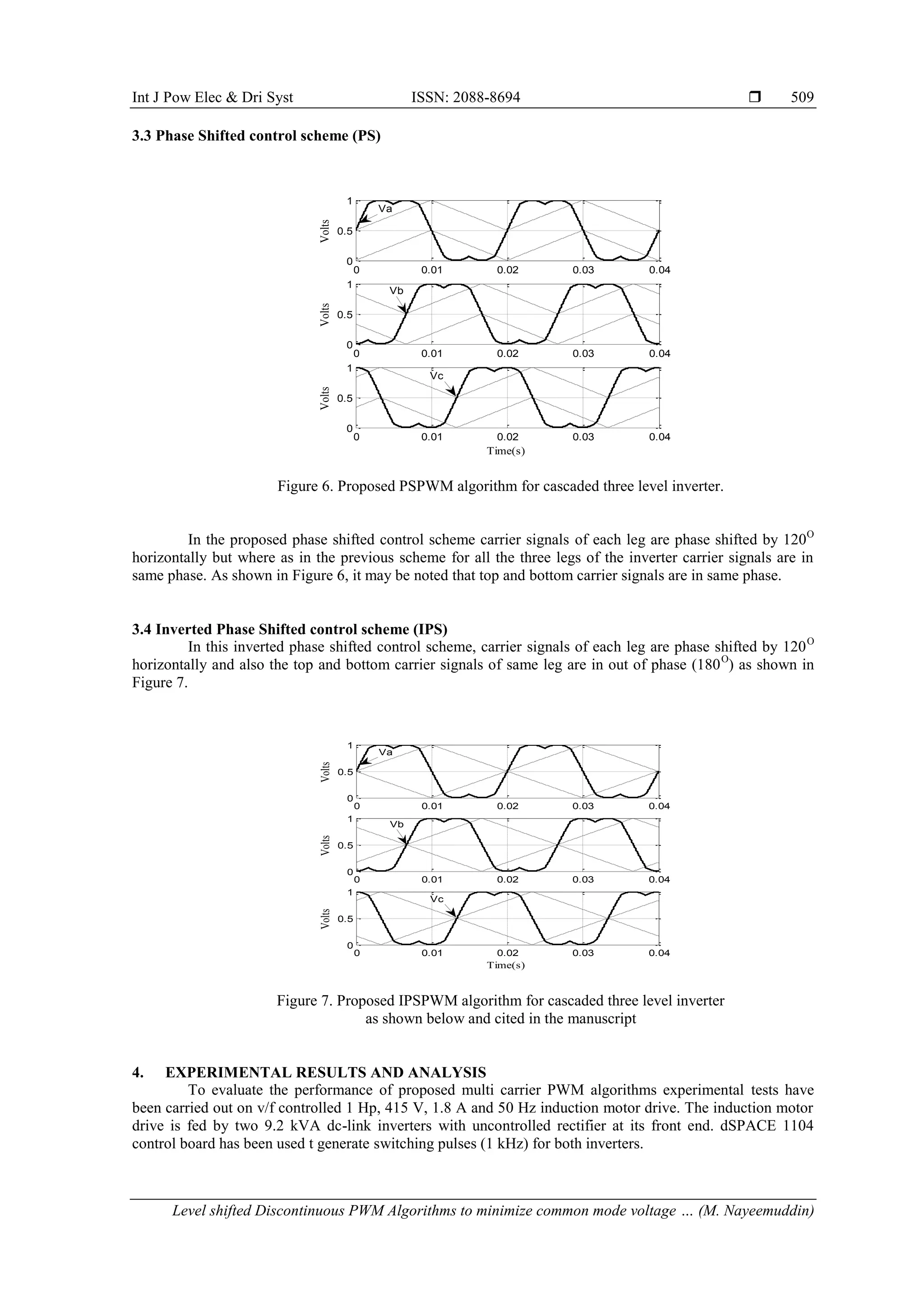
3. MULTI CARIER CONTROL STRATEGIES
Together with the development of multilevel inverter topologies appeared the challenge to extend
traditional modulation methods to the multilevel case. The switching frequency can subdivide multilevel
modulations into three different classes, namely, fundamental, mixed and high switching frequency.
Fundamental switching frequency modulations produce switch commutations at output fundamental
frequency and can be aimed to cancel some particular low frequency harmonic while, mixed switching
frequency modulations are those in which switches commutate at different frequency, like hybrid multilevel
modulation, and are particularly suited for hybrid converters, different cells can easily commutate at different
frequencies. And finally, high switching frequency modulations are the adaptation of standard PWM to
multilevel and they are meant to switch at very high frequency, about 10 to 20 kHz [16]-[18]. But this paper
focus only on some high frequency switching control schemes such as CC, IC, PS and IPS.
3.1 Common Carrier Control Scheme (CC)
Common carrier control scheme as shown in Figure 4 is one of the PWM technique for multilevel
inverter. For N level inverter N-1 in-phase carriers and a reference signal with the amplitude Am and the
frequency Fm (50 or 60 Hz) are required.
Figure 4. Proposed CCPWM scheme for cascaded three level inverter.
The control concept is the top carrier and bottom carrier signal are in phase with each other and are
compare with a three phase reference signals given in equation (5) to obtain three level operation. Top carrier
signal generates the pulse pattern for inverter-1 and similarly bottom carrier signal generates pulse pattern for
inverter-2.
3.2 Inverted Carrier Control Scheme (CC)
In inverted carrier control scheme as shown Figure 5, top carrier and bottom carrier signal are in out
of phase (180O
) with each other and are compared with a three phase reference signals given in equation (5)
to obtain three level operation. Top carrier signal generates the pulse pattern for inverter-1 and similarly
bottom carrier signal generates pulse pattern for inverter-2.
Figure 5. Proposed ICPWM algorithm for cascaded three level inverter
0 0.01 0.02 0.03 0.04
0
0.5
1
Time(s)
Volts
0 0.01 0.02 0.03 0.04
0
0.5
1
Time(s)
Volts](https://image.slidesharecdn.com/0410apr1812jan1810536-14679-1-ededitlelli-210611040025/75/Level-Shifted-Discontinuous-PWM-Algorithms-to-Minimize-Common-Mode-Voltage-for-Cascaded-Multilevel-Inverter-Fed-Induction-Motor-Drive-5-2048.jpg)
![ ISSN: 2088-8694
Int J Pow Elec & Dri Syst, Vol. 9, No. 2, June 2018 : 504 – 518
516
Figure 42. Phase Shifted Control Scheme at
Mi=0.81: Common mode voltage :DPWM
Figure 47. Inverted Phase Shifted Control Scheme
at Mi=0.81: Common mode voltage: DPWM
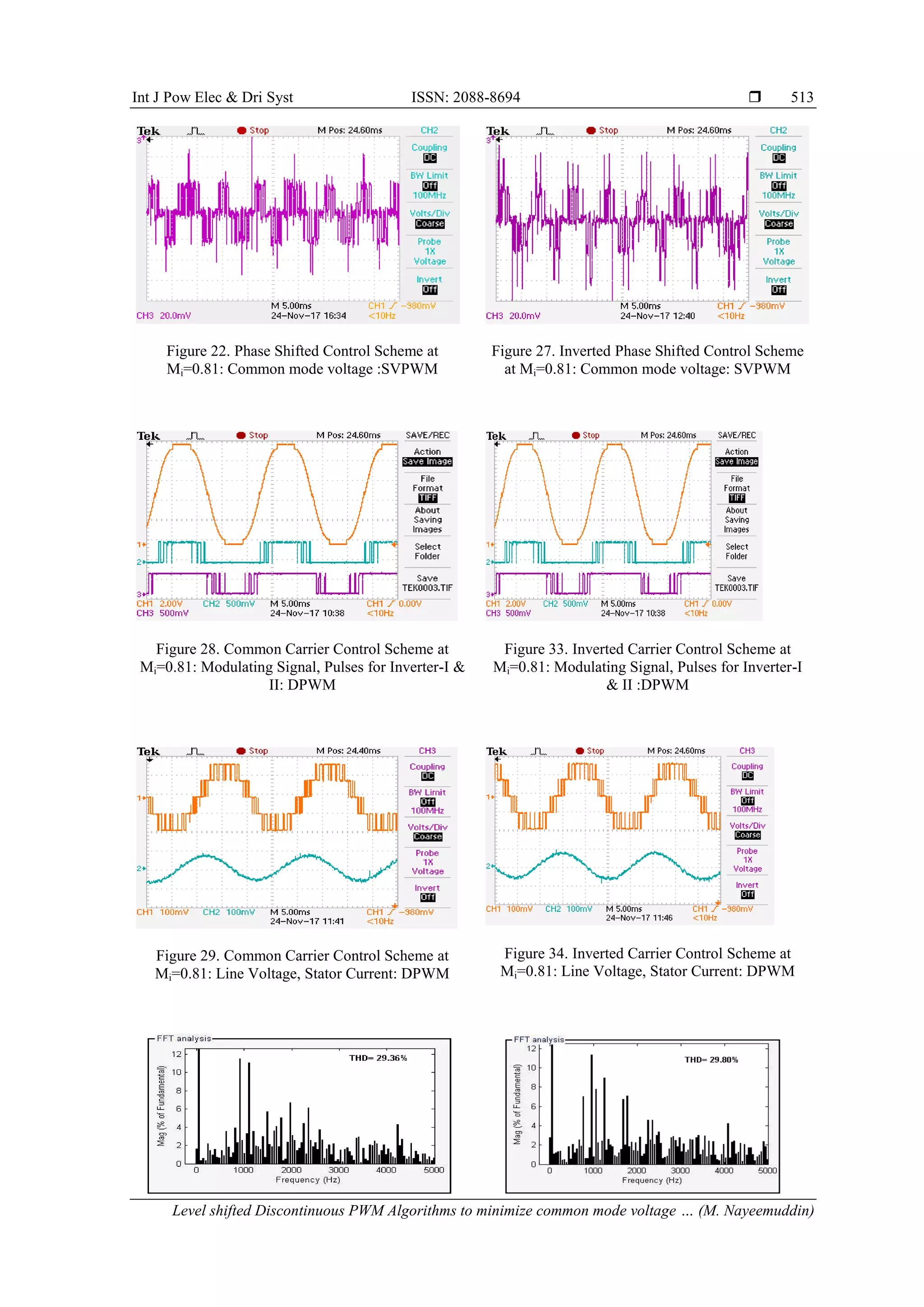
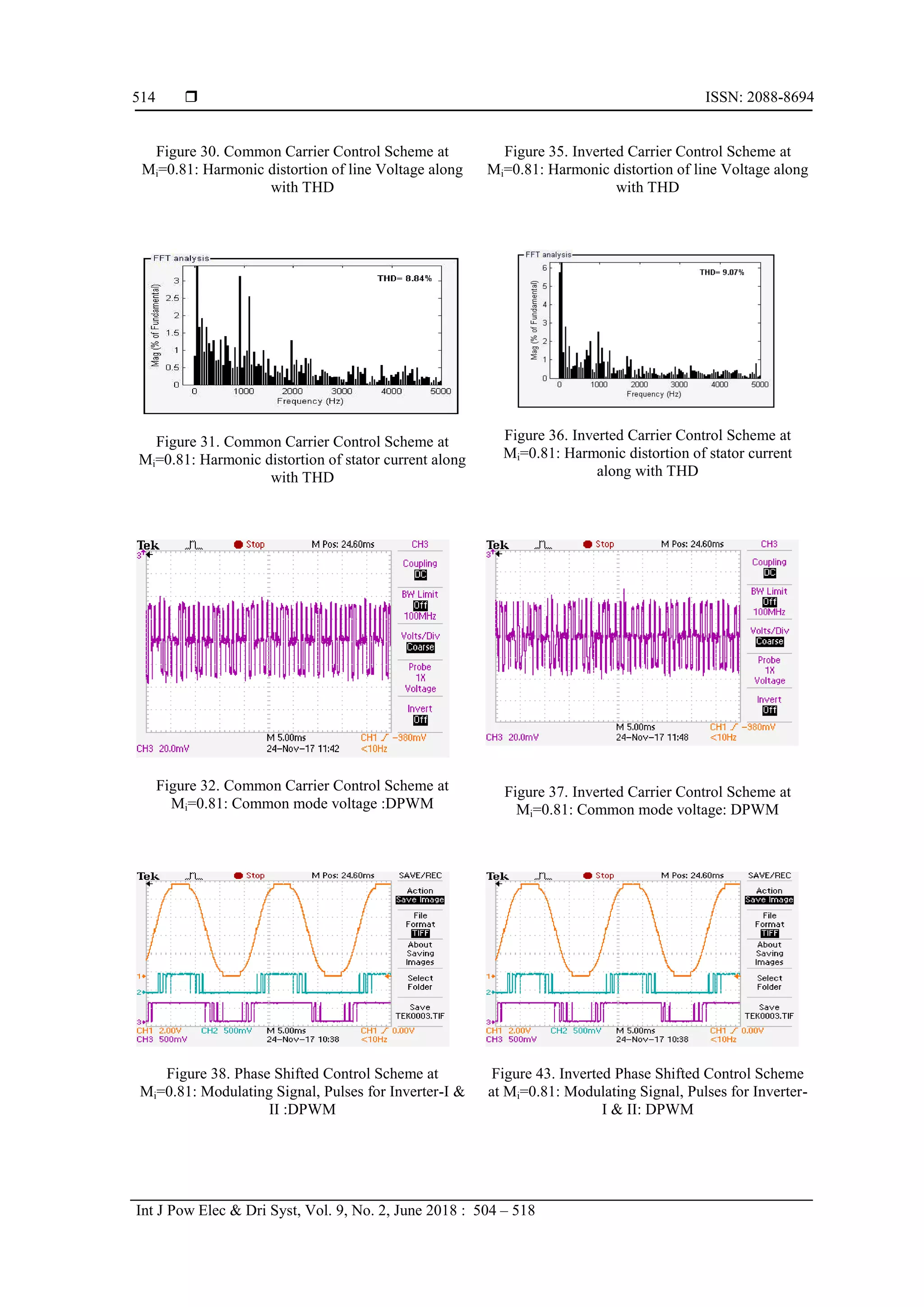
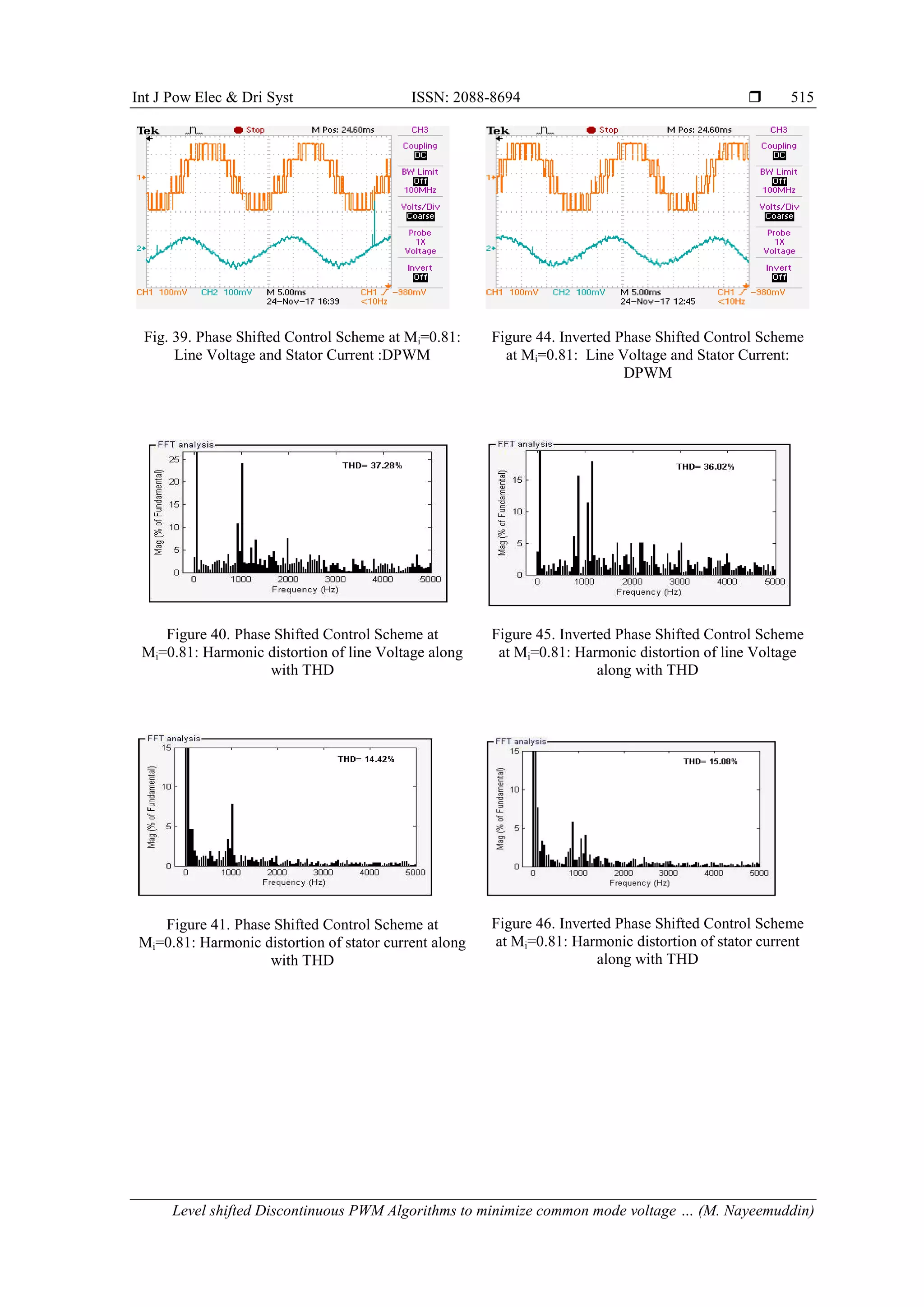
From the experimental results it is observed that with discontinuous modulating signal, the
switching of inverter has been reduced as well as its switching losses, as DPWM algorithm clamp for a total
period of 120 degrees in each fundamental cycle, the switching losses can be reduced to 33.33%.
As the proposed inverter configuration is capable of generating three level output it is observed in
that the effective pole voltage with different PWM algorithms contains three level (0 ,Vdc/2 and Vdc) for an
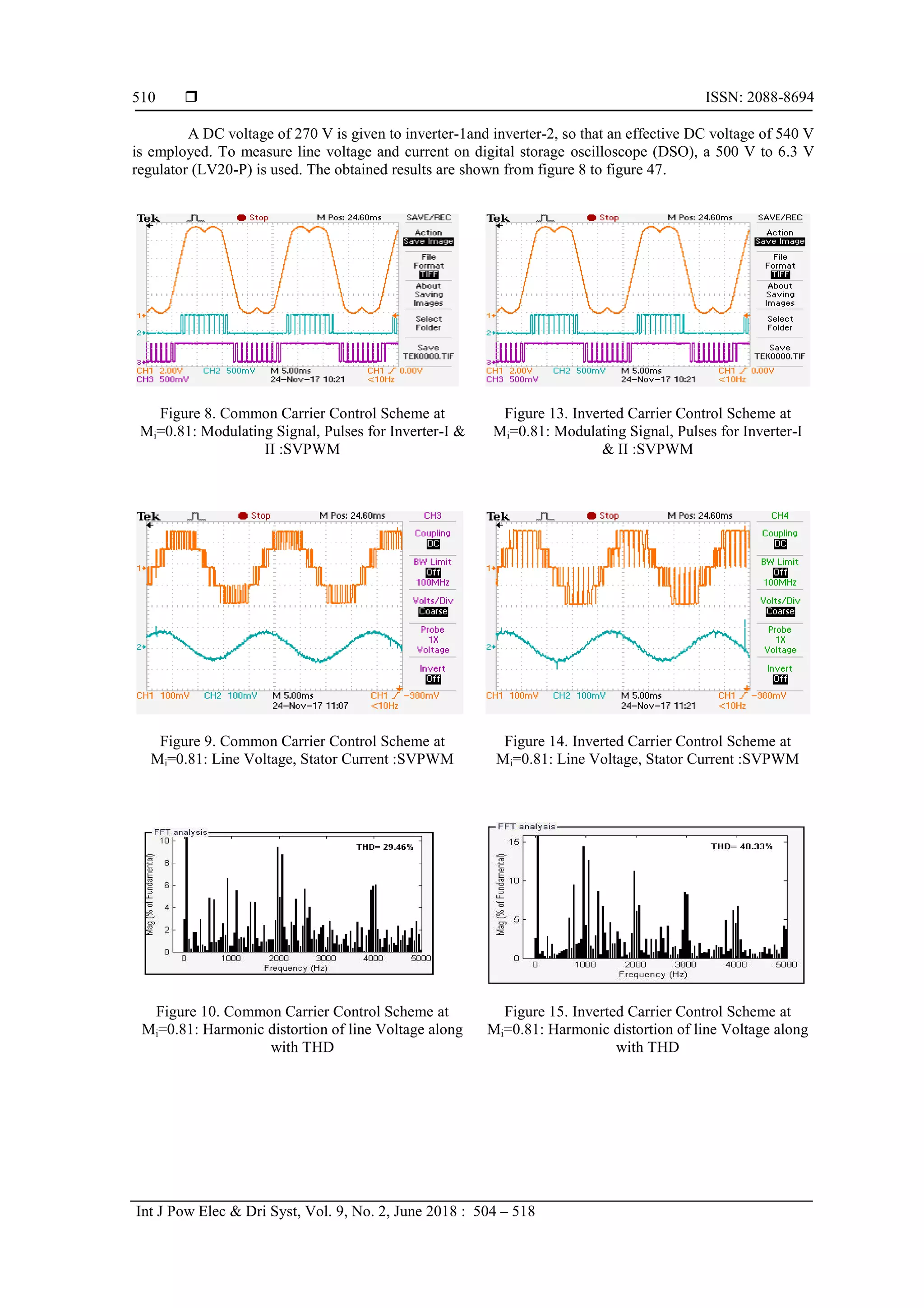
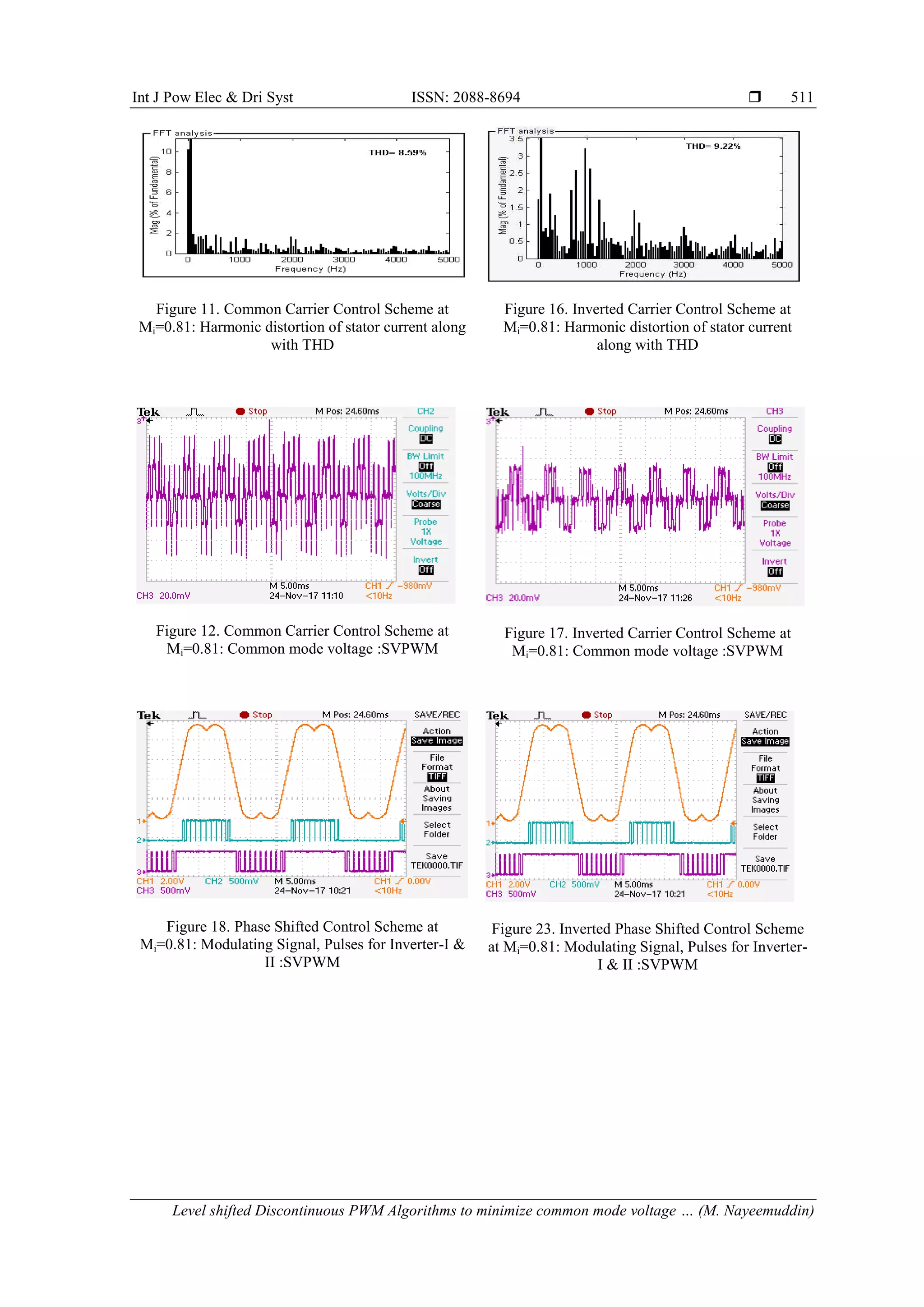
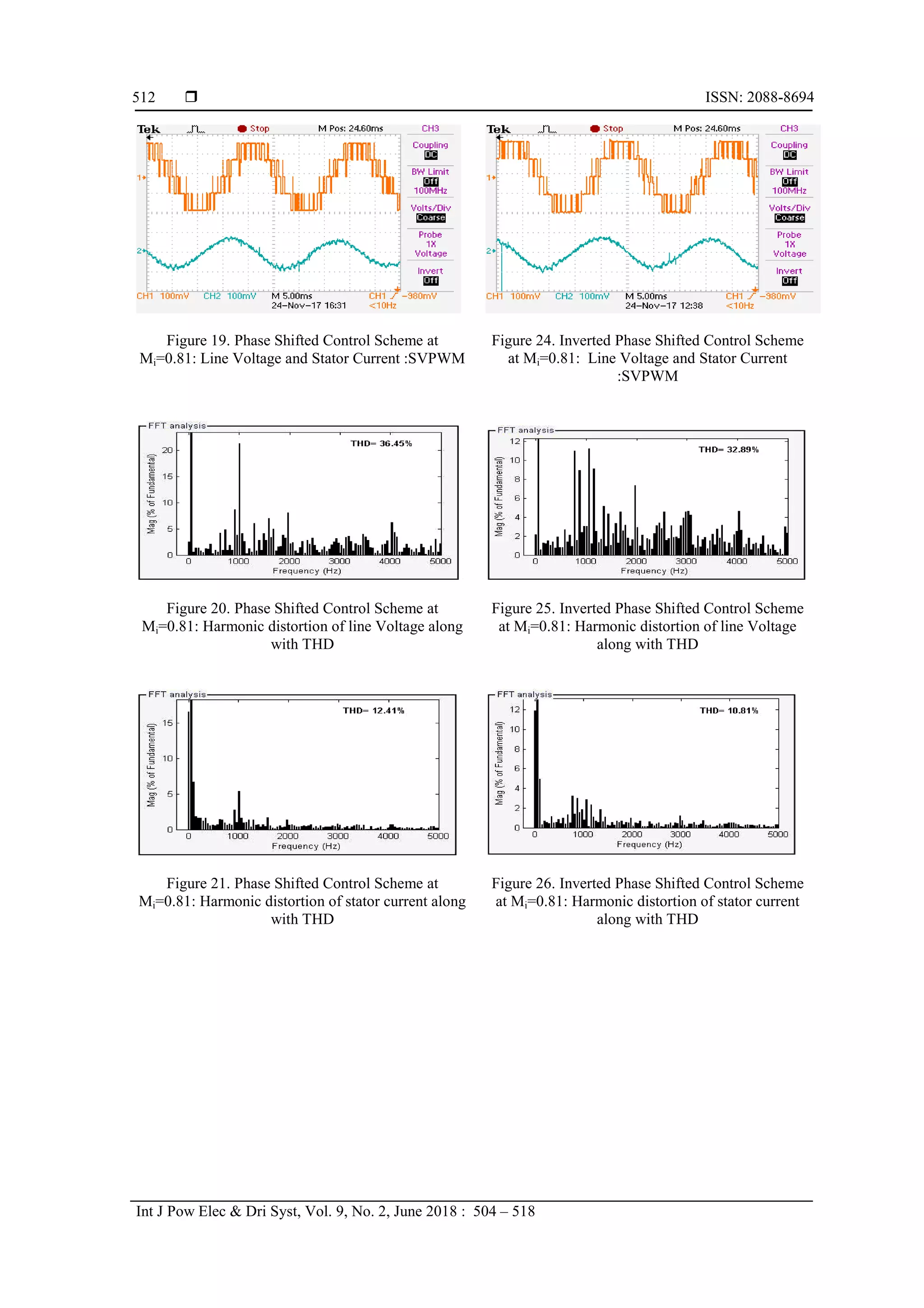
input DC voltage of 540V. Figure 8 to Figure 47 shows eualvation of four various multi carrier control
schemes and experimental results shows that common carrier based conventional SVPWM algorithm causes
a higher common mode voltage of 2Vdc/3 to -2Vdc/3 (i.e 180Volts to -180Volts) shown in figure 12, which
causes motor bearing currents effecting motor performance. However experimental results validates that by
using proposed inverted carrier control scheme common mode voltage is reduced from 2Vdc/3 to 2Vdc/6 (i.e
180Volts to 90 Volts). Therefore, the CMV is reduced by 50% with the discontinuous modulating signal
based inverted carrier control schemes. The FFT analysis was carried out for the line votage and phase
current and the total harmonic distortion (THD) for various control schems is presented and it is observed
that among various control schemes, inverter carrier control scheme minizes common mode voltgage with
fewer harmonic distortions.
5. CONCLUSION
This paper reviews multi carrier based simplified discontinuous PWM techniques for cascaded three
level inverter fed v/f controlled induction motor drive. Space vector approach requires angle and sector
information which increases complexity of the algorithm burden on the processor for program execution, but
whereas by using carrier comparison approach, the same modulating control signals have been obtained
without calculating angle and sector. This can be achieved by adding a zero sequence signal to the sinusoidal
reference signals. In this paper four various multi carrier control schemes have been evaluated and
experimental results are presented. From the results it is concluded that common carrier control scheme gives
fewer harmonic distortion but gives higher common mode voltage 2Vdc/3 which causes motor bearing
currents effecting motor performance. More over the proposed later schemes reduce higher common mode
voltage from 2Vdc/3 to 2Vdc/6 with less harmonic content. Finally it can concluded that among all the four
control schemes inverted carrier control scheme gives lesser harmonic with reduced common mode voltage.
This paper also concludes that continuous PWM algorithm give continuous pulse pattern which causes in the
increment of switching losses of the inverter, where as DPWM algorithms clamp to either positive dc bus or
negative dc bus for a total period of 120o
in every fundamental cycle. Hence, the DPWM algorithms reduce
the switching losses of the inverter by 33.33% along with common mode voltage reduction.
REFERENCES
[1] Holtz, J,“Pulse width modulation for electronic power conversion”, in Proc. IEEE, vol. 82, pp.1194–1214,Aug.
1994,.
[2] Sandeep Ojha, Ashok Kumar Pandey, “Close Loop V/F Control of Voltage Source Inverter using Sinusoidal PWM,
Third Harmonic Injection PWM and Space Vector PWM Method for Induction Motor”, International Journal of
Power Electronics and Drive Systems, vol. 7, No:1, pp 217-224, 2016](https://image.slidesharecdn.com/0410apr1812jan1810536-14679-1-ededitlelli-210611040025/75/Level-Shifted-Discontinuous-PWM-Algorithms-to-Minimize-Common-Mode-Voltage-for-Cascaded-Multilevel-Inverter-Fed-Induction-Motor-Drive-13-2048.jpg)
![Int J Pow Elec & Dri Syst ISSN: 2088-8694
Level shifted Discontinuous PWM Algorithms to minimize common mode voltage … (M. Nayeemuddin)
517
[3] C. Bharatiraja, et.al, “ Comparative Analysis of Different PWM Techniques to Reduce the Common Mode
Voltage in Three-Level Neutral-Point- Clamped Inverters for Variable Speed Induction Drives” , International
Journal of Power Electronics and Drive Systems, vol. 3, No:1, , pp 105-116, 2013.
[4] Fei Wang, " Sine-Triangle versus space vector modulation for three level PWM voltage sourceinverters",1EEE
Trans.lnd Applicat.,vol. 38,no. 2, March 2002.
[5] Dae-Woong Chung, Joohn-Sheok Kim, Seung-Ki Sui, "Unified Voltage Modulation Technique for Real-Time
Three-Phase Power Conversion" IEEE Trans. On Ind. Applications, vol. 34, no.2, pp 374-380, 1998.
[6] K. Satyanarayana, B. Anjaneyulu, K. Siva Prasad , “Performance Improvement of Multi Level Inverter fed Vector
Controlled Induction Motor Drive for Low Speed Operations”, International Journal of Power Electronics and
Drive Systems, Vol vol. 4, No:1, 2014.
[7] M. Malinowski, K. Gopakumar, J. Rodriguez, Pe, x, and M. A. rez, "A Survey on Cascaded Multilevel Inverters,"
Industrial Electronics, IEEE Transactions on, vol. 57, pp. 2197-2206, 2010.
[8] K. Ding, Z. Yun-ping, W. Zhan, W. Zhi-chao, and Z. Yun, "A novel hybrid diode-clamp cascade multilevel
converter for high power application," in Industry Applications Conference, 2004. 39th IAS Annual Meeting.
Conference Record of the 2004 IEEE, pp. 820-827 vol.2, 2004.
[9] J. Rodriguez, S. Bernet, W. Bin, J. O. Pontt, and S. Kouro, "Multilevel Voltage-Source-Converter Topologies for
Industrial Medium-Voltage Drives," Industrial Electronics, IEEE Transactions on, vol. 54,pp. 2930-2945, 2007.
[10] Gianluca Sena1 et.at., “A Comparative Study of Power Semiconductor Devices for Industrial”, International
Journal of Power Electronics and Drive Systems, Vol. 7, No:4, pp. 1-8,2016.
[11] A. Nabae, I. Takahashi and H. Akagi, “A new neutral point clamped PWM inverter”, IEEE Trans. Ind. Appl.,
17(5), pp 518–522, 1981.
[12] Edison Roberto C.DA Silva, Euzeli Cipriano Dos Santos, Hr and Cursino Brandao Jacobina “Pulse width
Modulation Strategies: Non sinusoidal Carrier Based PWM and space vector Modulation Techniques” IEEE
Industrial Electronics Magazine, pp. 37-45, June 2011
[13] Kureve D. Teryima, Goshwe Y. Nentawe, Agbo O. David, “A Overlapping Carrier Based SPWM for a 5-Level
Cascaded H-bridge Multilevel Inverter”, International Journal of Power Electronics and Drive Systems, Vol vol. 7,
No:2, 2016.
[14] Lixiang Wei; Guire, J.M.C.; Jiangang Hu “Novel discontinuous PWM control method to improve IGBT reliability
at low speed Energy Conversion”Congress and Exposition (ECCE), pp.3819 - 3825, 2014 IEEE.
[15] Edison Roberto C.DA Silva, Euzeli Cipriano Dos Santos, Hr and Cursino Brandao Jacobina “Pulse width
Modulation Strategies: Non sinusoidal Carrier Based PWM and space vector Modulation Techniques” IEEE
Industrial Electronics Magazine, pp. 37-45, June 2011.
[16] Shaoliang An; Xiangdong Sun; Yanru Zhong; Matsui, M. “Research on a new and generalized method of
discontinuous PWM strategies to minimize the switching loss”, Innovative Smart Grid Technologies - Asia (ISGT
Asia), Pages: 1 – 6, 2012 IEEE
[17] J. Amarnath*, A. Kailasa Rao**, K. Satyanarayana*, "Novel AZSPWM Algorithms based VCIMD for Reduced
CMV Variations" , International Journal of Power Electronics and Drive Systems, Vol vol. 3, No:1, pp. 1-8, 2013.
[18] B. P. McGrath and D. G. Holmes, "Multicarrier PWM strategies for multilevel inverters,"Industrial Electronics,
IEEE Transactions on, vol. 49, pp. 858-867, 2002.
BIOGRAPHIES OF AUTHORS
Nayeemuddin.M had completed his B.Tech and M.Tech in 2005 and 2008 with first
class in the department of Electrical and Electronics Engineering from
J.N.T.University Hyderabad and Sri Krishna Devaraya. University Ananthapuramu
respectively. Now he is pursuing his Ph.D in J.N.T. University, Ananthapuramu. He is
working as a Assistant Professor in the Department of Electrical and Electronics
Engineering. His scientific research is focusing on Power Electronics, and Motor Drive
control.
Dr. T. Bramhananda Reddy had completed his B.Tech and M.E in 2001 and 2003 with
first class in the department of Electrical and Electronics Engineering from Sri Krishna
Devaraya University Ananthapuramu and Osmania University, Hyderabad
respectively. He obtained doctoral degree from J.N.T. University, Ananthapuramu in
2009. He is working as a Professor and Head of the department of Electrical and
Electronics Engineering in G.P.R Engineering College, Kurnool. He presented more
than 120 research papers in various national and international conferences and journals.
His research areas include PWM techniques, Power Electronics and control of
electrical drives.](https://image.slidesharecdn.com/0410apr1812jan1810536-14679-1-ededitlelli-210611040025/75/Level-Shifted-Discontinuous-PWM-Algorithms-to-Minimize-Common-Mode-Voltage-for-Cascaded-Multilevel-Inverter-Fed-Induction-Motor-Drive-14-2048.jpg)