Abstract: In this paper, a simulation of SPWM (Unipolar) strategy is presented for Single phase full bridge inverter. The model is simulated in Matlab/Simulink. For different power factor loads the % THD of the output voltage are observed. The change in modulation index (MI) and the frequency of the carrier signal (f_c) changes the % THD of the output voltage. The width of gate pulses are modulated in order to obtain controlled inverter out voltage and to reduce the harmonic content as well. A comparative study of the % THD of the output voltage for the same load when connected across a conventional inverter and across SPWM fed inverter helps to understand the performance of the inverter. In SPWM inverter, to generate the gate signals, triangle wave is the carrier wave which is compared with the reference sinusoidal wave. The frequency of the output voltage depends on the frequency of the reference wave.
Bhosari ( Call Girls ) Pune 6297143586 Hot Model With Sexy Bhabi Ready For ...
Harmonic Distortion Analysis of the Output Voltage in SPWM (Unipolar) Single Phase Full Bridge Inverter
1. ISSN 2349-7815
International Journal of Recent Research in Electrical and Electronics Engineering (IJRREEE)
Vol. 3, Issue 2, pp: (34-38), Month: April 2016 - June 2016, Available at: www.paperpublications.org
Page | 34
Paper Publications
Harmonic Distortion Analysis of the Output
Voltage in SPWM (Unipolar) Single Phase Full
Bridge Inverter
1
Nidhi Gupta, 2
Ashish Choubey
1
M.E. Student (HVPS Engg), 2
Assistant Professor, Deptt. of Electrical Engineering, JEC Jabalpur, M.P., India
Abstract: In this paper, a simulation of SPWM (Unipolar) strategy is presented for Single phase full bridge
inverter. The model is simulated in Matlab/Simulink. For different power factor loads the % THD of the output
voltage are observed. The change in modulation index (MI) and the frequency of the carrier signal ( ) changes
the % THD of the output voltage. The width of gate pulses are modulated in order to obtain controlled inverter out
voltage and to reduce the harmonic content as well. A comparative study of the % THD of the output voltage for
the same load when connected across a conventional inverter and across SPWM fed inverter helps to understand
the performance of the inverter. In SPWM inverter, to generate the gate signals, triangle wave is the carrier wave
which is compared with the reference sinusoidal wave. The frequency of the output voltage depends on the
frequency of the reference wave.
Keywords: Sinusoidal pulse width modulation (SPWM), Unipolar, Total Harmonic distortion (THD), Order of
Harmonics, lagging and leading pf loads.
I. INTRODUCTION
Inversion is the process of conversion dc power to ac power at a required output voltage, current and frequency. A static
semiconductor performs this electrical energy inverting transformation process. The inverter receives the DC power from
a battery and then converts it to AC with the desirable frequency. The inverter is therefore adjustable frequency voltage
source.
Inverters can be classified in two types:
voltage sorce inverter (VSI)
Current source inverter (CSI).
A voltage source inverter (VSI) is the one in which the DC input voltage is constant and is independent of the current
drawn by the load. In VSI the dc source has small or negligible impedance. The voltage at the input terminals of inverter
is always constant. A current source inverter (CSI) is fed with adjustable current from the dc source of high impedance
that is from a constant dc source.
According to the connections of semiconductor devices, inverters are:
Bridge Inverters
Series Inverters
Parallel Inverters
2. ISSN 2349-7815
International Journal of Recent Research in Electrical and Electronics Engineering (IJRREEE)
Vol. 3, Issue 2, pp: (34-38), Month: April 2016 - June 2016, Available at: www.paperpublications.org
Page | 35
Paper Publications
A voltage source inverter (VSI) using thyristor as a switch requires forced commutation, while the VSI in which
MOSFET, GTO, IGBT, power transistors are the switching devices, self commutation with gate pulse is required for their
controlled turn on and off process.
II. SINUSOIDAL PULSE WIDTH MODULATION (SPWM)
Pulse width modulation (PWM) is a powerful technique to controlling the switching devices in inverter circuits. PWM
provides a way to decrease the Total Harmonic Distortion (THD) of load current and output voltage. The THD
requirement can be met more easily when the output of PWM inverter is filtered. The unfiltered output will have
relatively high THD, but the harmonic will be at the much higher frequencies which can be filtered out easily.
Sinusoidal pulse width modulation (SPWM) is a very simple technique used for harmonic reduction. In this technique a
carrier wave (Triangular) is compared with a reference wave (Sinusoidal) to generate the gate pulses for the inverter.
A sinusoidal reference wave , reference wave with phase shift and a triangular carrier wave of higher
frequency are compared for gate pulses. There are two important parameters in this modulation technique:
Amplitude Modulation Ratio or Modulation Index (MI)
Frequency Modulation Ratio
Amplitude Modulation ratio =
Frequency Modulation ratio =
The rms output voltage can be varied by varying the modulation index MI. Frequency modulation ratio changes the
number of gating pulses per half cycle of the reference wave. It can be controlled by varying the frequency of carrier
signal . This type of modulation eliminates all harmonics less than or equal to 2P – 1. Where P is the number of pulses
per half cycle = .
THD is a measure of closeness in shape between a waveform and its fundamental component. THD gives the information
about total harmonic content, but it dose not indicate the level of each harmonic component. Lowest order harmonic
(LOH) is that harmonic component whose frequency is closest to the fundamental one, and its amplitude is greater than or
equal to 3% of the fundamental component.
III. SIMULATION RESULTS
Fig.1: Triggering pulses for SPWM Unipolar Full Bridge Inverter
3. ISSN 2349-7815
International Journal of Recent Research in Electrical and Electronics Engineering (IJRREEE)
Vol. 3, Issue 2, pp: (34-38), Month: April 2016 - June 2016, Available at: www.paperpublications.org
Page | 36
Paper Publications
THD analysis of output voltage and current in a conventional full wave bridge inverter supplied by 240V DC source at
constant load variable power factor:
Load THD load current THD output voltage
5kw 0 pf lag 12.1 %
48.35%
5kw 0.6 pf lag 14.74 %
5kw 0.8pf lag 18.66 %
5kw unity pf 48.35 %
5kw 0.8pf lead 59.43 %
5kw 0.6pf lead 76.6 %
5kw 0 pf lead 84.59 %
It is clear from the above results that THD of the current depends upon the load pf. Harmonic distortion of current is high
for a purely capacitive load and it is minimum for a purely inductive load. The THD of the output voltage is independent
from the load power factor.
A 5 kw 0.8 lag pf load is connected to a 240V DC sources supplied single phase spwm fed unipolar full bridge inverter.
For different values of carrier frequency THD analysis of the output voltage is shown by the tables below:
Table 1
For MI = 1 and = 50 Hz
= 240 volts , = 48.35 %
Voltage profile of the out put voltage
Harmonic Order DC component 3 5 7 9 11 13 All even order harmonics are 0.39
% of fundamental component% of fundamental 0.19 33.33 20 14.28 11.1 9.08 7.68
Table 2
For = 300 Hz and MI = 0.6
= 105.57 volts , = 105.57 %
Voltage profile of the out put voltage
Harmonic Order DC component 3 5 7 9 11 13
% of fundamental 0 4.79 0.14 2.51 12.14 64.35 62.76
Table 3
For = 300 Hz and MI = 1
= 188.2 volts , = 49.92 %
Voltage profile of the out put voltage
Harmonic Order DC component 3 5 7 9 11 13
% of fundamental 0 1.28 0.95 2.18 22.27 19.08 18.06
Table 4
For = 500 Hz and MI = 0.6
= 147 volts , = 107.82 %
Voltage profile of the out put voltage
Harmonic Order DC component 3 5 7 9 11 13
% of fundamental 0 3.12 1.45 3.12 1.5 3.24 0.71
Table 5
For = 500 Hz and MI = 1
= 188.2 volts , = 55 %
Voltage profile of the out put voltage
Harmonic Order DC component 3 5 7 9 11 13
% of fundamental 0 1.62 0.37 1.58 0.11 0.11 0.48
4. ISSN 2349-7815
International Journal of Recent Research in Electrical and Electronics Engineering (IJRREEE)
Vol. 3, Issue 2, pp: (34-38), Month: April 2016 - June 2016, Available at: www.paperpublications.org
Page | 37
Paper Publications
Fig.2: Output voltage Harmonic spectra for = 50 Hz and MI = 1
Fig.3: Output voltage Harmonic spectra for = 300 Hz and MI = 0.6
Fig.4: Output voltage Harmonic spectra for = 300 Hz and MI = 1
5. ISSN 2349-7815
International Journal of Recent Research in Electrical and Electronics Engineering (IJRREEE)
Vol. 3, Issue 2, pp: (34-38), Month: April 2016 - June 2016, Available at: www.paperpublications.org
Page | 38
Paper Publications
Fig.5: Output voltage Harmonic spectra for = 500 Hz and MI = 0.6
Fig.6: Output voltage Harmonic spectra for = 500 Hz and MI = 1
IV. CONCLUSION
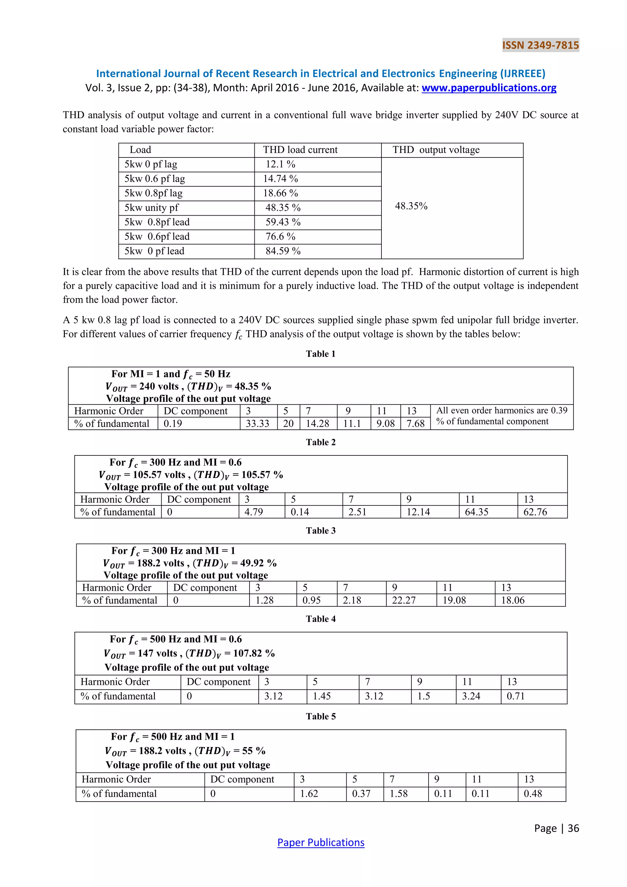
From the results shown in table 1 to table 5 and harmonic spectra of the output voltage shown in fig.2 to fig.6, following
conclusions can be drawn:
1. For a lagging power factor load, the output voltage contains odd harmonics in significant % of the fundamental
component. The even harmonics are not in a significant % of fundamental component.
2. To reduce the THD of the output voltage the frequency of carrier signal and the modulation index MI plays the key
role. On changing the (MI) from 0.6 to 1, output voltage THD reduces from 105% to 49% at a carrier frequency 300 Hz.
To eliminate any particular order of harmonics carrier frequency is the key factor. At carrier frequency = 300 Hz ,
lower order harmonics are reduced as compare to their % for 50 Hz carrier frequency. On changing the modulation index
(MI) from 0.6 to 1 on the same carrier frequency, the % of the odd harmonics goes down significantly.
3. The same trend of results can also be observed for = 500 Hz and for MI = 0.6 & 1..
4. The magnitude of the output voltage varies with change in MI. It increases as MI approaches to the higher value i.e. 1.
REFERENCES
[1] Muhammad H.Rashid, Third edition, “Power electronics circuits,devices and applications”,Practice Hall of India.
[2] M D Singh, K.B.Khanchandani, Second edition, “Power electronics”,Tata McGraw Hill Education Private Limited.
[3] Bose K.B.(1997) , “Power electronics and Variable frequency Drives”, IEE Press ISBN 0-7803-1061-6, New York.