The document presents a comparative analysis of pulse width modulation (PWM) techniques for three-level diode clamped voltage source inverters, focusing on sine PWM (SPWM) and space vector PWM (SVPWM). The paper introduces a simplified SVPWM algorithm that enhances control over diode clamped inverters and reduces total harmonic distortion (THD) compared to conventional methods. Simulation results demonstrate that the proposed SVPWM control outperforms SPWM in terms of THD and can be effectively applied to various multilevel inverter configurations.
![International Journal of Power Electronics and Drive System (IJPEDS)
Vol. 5, No. 1, July 2014, pp. 15~23
ISSN: 2088-8694 15
Journal homepage: http://iaesjournal.com/online/index.php/IJPEDS
Comparative Analysis of PWM Techniques for Three Level
Diode Clamped Voltage Source Inverter
Zulkifilie Bin Ibrahim, Md. Liton Hossain, Ismadi Bin Bugis, Jurifa Mat Lazi, Nurazlin Mohd Yaakop
Department of Power Electronics and Drive, Faculty of Electrical Engineering, Universiti Teknikal Malaysia Melaka,
Melaka, Malaysia
Article Info ABSTRACT
Article history:
Received Mar 30, 2014
Revised May 22, 2014
Accepted Jun 1, 2014
Multilevel inverters are increasingly being used in high-power medium
voltage industrial drive applications due to their superior performance
compared to conventional two-level inverters. Thre are a number of Pulse
width modulation (PWM) techniques applied in recent years. The most
widely applied PWM techniques are Sine Pulse Width Modulation (SPWM)
and Space Vector Pulse Width Modulation (SVPWM). SPWM is the most
simple modulation technique that can realize easily in analog circuit.
However, it has some drawbacks such as higher total harmonic distortion
(THD), lower effective DC utilization and lower switching frequency. Space
vector pulse width modulation (SVPWM) is widely used because of their
easier digital realization and better DC bus utilization and lower THD. The
complexity is due to the difficulty in determining the reference vector
location, on times calculation, and switching states selection. This paper
presents a simple SVPWM algorithm for diode clamped three level inverters
based on standard two-level SVPWM which can easily determine the
location of reference vector, calculate the on-times, the selection of switching
states. Three level diode clamped inverter (3LDCI) using space vector
modulation technique has been modeled and simulated using
MATLAB/SIMULINK and Origin 6.1 with a passive R-L load that can be
extended to any level. Simulation results are presented to verify the proposed
SVPWM control in terms of THD. The results arecompared with
conventional sinusoidal pulse width modulation (SPWM) where SVPWM
shows better performance than SPWM in terms of THD.
Keyword:
3LDCI
Multilevel inverter
Pulse width modulation
SPWM
SVPWM
THD
Copyright © 2014 Institute of Advanced Engineering and Science.
All rights reserved.
Corresponding Author:
Zulkifilie Bin Ibrahim,
Associate Professor,
Department of Power Electronics and Drive,
Faculty of Electrical Engineering, Universiti Teknikal Malaysia Melaka,
Hang Tuah Jaya, 76100 Durian Tunggal, Melaka, Malaysia.
Email: drzulkifilie@utem.edu.my
1. INTRODUCTION
Multilevel inverter technology has emerged recently as a very important alternative in the area of
high-power medium voltage energy control. Today, it is hard to connect a single power semiconductor switch
directly to medium voltage grids. Harmonic distortion is high for conventional inverter. For these reasons, a
new family of diode clamped multilevel inverters has emerged as the solution for working with higher
voltage levels and lower harmonic distortion [1]. Rodríguez and Lai discussed several multi-level inverter
topologiesto increase the power delivered to the load and toimprove the quality of the voltage [2]. In this
paper, a diode clamped three level voltage source inverter is presented. This clamping diode can produce
additional voltage level that reduces the harmonic distortion.](https://image.slidesharecdn.com/0222may14id6038comparativeanalysisofpwmedit-171213054032/75/Comparative-Analysis-of-PWM-Techniques-for-Three-Level-Diode-Clamped-Voltage-Source-Inverter-1-2048.jpg)
![ ISSN: 2088-8694
IJPEDS Vol. 5, No. 1, July 2014 : 15 – 23
16
A variuspulse width modulation (PWM) techniques have been discussed to control the inverter [3].
Among these modulation techniques for a multilevel inverter, SVPWM is the most popular technique due to
their unique characteristics such as directly using the control variable, improving DC link voltage utilization,
reducing commutation losses and THD, easy DSP implementation and optimization of switching patterns [4],
[5]. The space vector diagram consists of six sectors for any level inverter. Each sector contains (m-1)2
triangles where m is the number of levelsin which the reference vector can be located within any of these
triangles. A switching vector comprising a number of switching states represents the vertices of each triangle.
There are m3
switching states for m-level inverter. The on time equations of SVPWM execute the switching
states of the triangle. The performance of the inverter significantly depends on the selection of these
switching states [6]. Triangle numbers, switching states increase with the increase of level that creates
computational complexity in terms of on time calculations. There are a number of space vector algorithms
that shows the better performance. Some of them some are mentioned with their limitations. Celanovic and
Boroyevich presented a euclidean vector system based SVPWM algorithm that needs several matrix
transformations, lacks of regular sequence of determining the switching states and is unsuitable for real-time
implementation [7]. The method proposed by Loh and Holmes [8] with two level on time calculation will
result in total computations higher than Celanovic and Boroyevich [7]. Authors [9] introduce a method for
on-time calculation that works well only up to three levels. The multilevel ON-time calculation problem is
converted to a simple two-level ON-time calculation problem. J. H. Seo and C. H. Choi [10] proposed a
technique for a three-levelinverter based on two level inverter.The three-level space vectordiagram is divided
into six two-level space vector diagrams. Atwo-phase to three-phase conversion is needed to calculate
thepoint to shift of origin of a virtual two-level inverter. Subsequentto the shift of origin and 600
coordinate
transformation,on-times are calculated using two-level equations. Even forthree levels, this techniquerequires
more computations thanthe presentedtechnique [6]. Trabelsiand Ben-Brahim [11] proposed a new space
vector algorithm that needed separate equations to calculate on times for odd and even number triangle
determination.
In this paper, we presented a simple algorithm to perform the SVPWM for diode clamped three
level inverter. The on-time calculation is based on two level SVPWM algorithm that is simple and the on-
time calculation equations do not change with the position of reference vector like the conventional
algorithm. In the space vector diagram of an m-level inverter, the triangle where the reference vector is
located is identified as integer ∆n. Any switching sequence can be executed with respect to triangle ∆n,
leading to an easiness and flexibility of optimizing the switching sequence. Three level space vector diagram
is divided into six sector each containing four triangle shown in figure 1.ShantanuChatterjee used 7 switching
states for triangle 1, 4 switching states for triangle 2 and 4 and 5 switching states for triangle 3 that needed
more memory space, more computation time and more lookup table [12]. In this control technique, there
have been proposed only four active switching states in each triangle shown in Table 1 that required less
number of lookup table and computations. This technique can be used for any m-level inverter without any
significant increase in computations.
Figure 1. Space vector diagram for three level inverter](https://image.slidesharecdn.com/0222may14id6038comparativeanalysisofpwmedit-171213054032/75/Comparative-Analysis-of-PWM-Techniques-for-Three-Level-Diode-Clamped-Voltage-Source-Inverter-2-2048.jpg)
![IJPEDS ISSN: 2088-8694
Comparative Analysis of PWM techniques for Three Level Diode Clamped Voltage… (Zulkifilie Bin Ibrahim)
17
2. SVPWM ALGORITHM
Nupur Mittal and Bindeshwar Singh presented different PWM techniques applied for controlling the
active devices in a multilevel inverter [13]. In this paper, SVPWM technique is presented to produce PWM
control signals to the inverter. SVPWM compensates the required volt-seconds using discrete switching
states and their on-times. The classical two-level space vector geometry can be used for on-time calculation.
The space vector diagram of a three phase voltage source inverter is a hexagon, consisting of six sectors.
Every sector is an equilateral triangle of unity side and h (=√3/2) is the height of a sector. The on-time
calculation is same for all sectors. Volt-second equation is:
(1)
The volt-seconds in terms of components VZ
, VX and VY of along axis are,
(2)
(3)
(4)
Solving Equation (2)–(4), obtain for the calculation of ON times,
(5)
(6)
(7)
Where Ts = 1/2fs, fs is the switching frequency.For any given reference vector, the sector of operation and its
angle within the sector is determined by using Equation (8) and (9), respectively.
1 (8)
(9)
In eqns. (8) and (9), 0 360 is the angle of the reference vector with respect to x-axis,
0 60 is the angle within the sector and 1 6 is its sector operation, int and rem are
standard math function of integer and reminder.
In each sector, triangle can be classified into two types. Type 1 triangle has its base side at the
bottom. Type 2 triangle has its base side at the top. The triangle number ∆ can be determined in terms of two
integer variables P1and P2, which are dependent on the position of reference vector , .
√
(10)
(11)
P1 represents the part of the sector between the two lines joining the vertices, separated by distance h
and inclined at 1200
with respect to axis shown in Figure 2. P1 = 0 signifies that the point Q is below line
A1A2. P1 = 1 signifies that the point Q is between line A1A2 and line A3A5. P2 represents the part of the sector
between the two lines joining the vertices, separated by distance h and parallel to axis. P2 = 0 signifies
that the point Q is between line A0A3 and line A2A4. P2 = 1 signifies that the point Q is above line
A2A4.Geometrically, the values of P1 and P2 are an intersection of two rectangular regions which is either a
triangle or rhombus. In other words, the point Q lies in (a) triangle ∆ if P1 =0 and P2 =0, (b) rhombus
A1A3A4A2 if P1 = 1 and P2 = 0, (c) triangle ∆ if P1 = 1 and P2 = 1. The same analogy can be used for any
level. In Figure 2, the reference vector is located in rhombus A1A3A4A2 .This rhombus is made up of two](https://image.slidesharecdn.com/0222may14id6038comparativeanalysisofpwmedit-171213054032/75/Comparative-Analysis-of-PWM-Techniques-for-Three-Level-Diode-Clamped-Voltage-Source-Inverter-3-2048.jpg)
![ ISSN: 2088-8694
IJPEDS Vol. 5, No. 1, July 2014 : 15 – 23
18
triangles ∆ and ∆ .The point Q can be located in any of the two. Let , be the coordinates of the point
Q with respect to the point A1 obtained as:
. 5 (12)
Figure 2. Space vector diagram of triangle determination for sector 1
(13)
In Equation (12) and (13), / is the slope of the line between the origin of the rhombus and
the reference vector and it is compared with slope of the diagonal of the rhombus which is√3.
The slope comparison is done by evaluating inequality √3 and to determine the small
vector VZ
and the exact triangle number ∆ . If √3 which indicates triangle of type 1 and these
triangles are similar to sector 1 of two-level inverter. The triangle number ∆ is obtained as:
∆ 2 (14)
If √3 which indicates triangle of type 2 and these triangles are similar to sector 2 of two-level
inverter. The triangle number ∆ is obtained as:
∆ 2 1 (15)
In Equation (14) and (15), ∆ indicates the triangle and n is the triangle number and hence ∆ is an
integer and signifiesnth triangle in the sector. Using eqns. (14) and (15), to identify triangle in a sector and
the on times are calculatedusing Equation (5)–(7). The ∆ is formulated to provide a simple way of arranging
the triangle, leading to ease of identification and extension to any level.
3. CONTROL TECHNIQUE AND TOPOLOGY
The multilevel inverter is best suited for the application which demands the finest quality of the ac
supply waveforms. This work presented a SVPWM control technique, which pertains full H-Bridge diode
clamped multilevel inverters. Some researcher used (m+1) number dc sources [4], [15] for developing their
proposed model that increase the cost as well as make the system bulky. In this model, we used (m-1)/2
number of dc sources that are cost effective. The general function of this multilevel inverter is to synthesize a
desired voltage from a single dc source which may be obtained from battery, fuel cell, or solar cell. Unlike
the cascaded inverter, the diodeclamp inverter does not require separate voltage sources for each half
bridge.A three phase three-level full H-bridge inverter is shown in Figure 3. An m-level three phase full H-
bridge inverter typically consists of 6(m- 1) main switching devices and 6(m-2) main diodes. A three phase
RL load of 50 ohm and 20 mH is connected across the output of inverter. The switching sequences for three
phase three level inverter are given in Table 2 [16].](https://image.slidesharecdn.com/0222may14id6038comparativeanalysisofpwmedit-171213054032/75/Comparative-Analysis-of-PWM-Techniques-for-Three-Level-Diode-Clamped-Voltage-Source-Inverter-4-2048.jpg)
![ ISSN: 2088-8694
IJPEDS Vol. 5, No. 1, July 2014 : 15 – 23
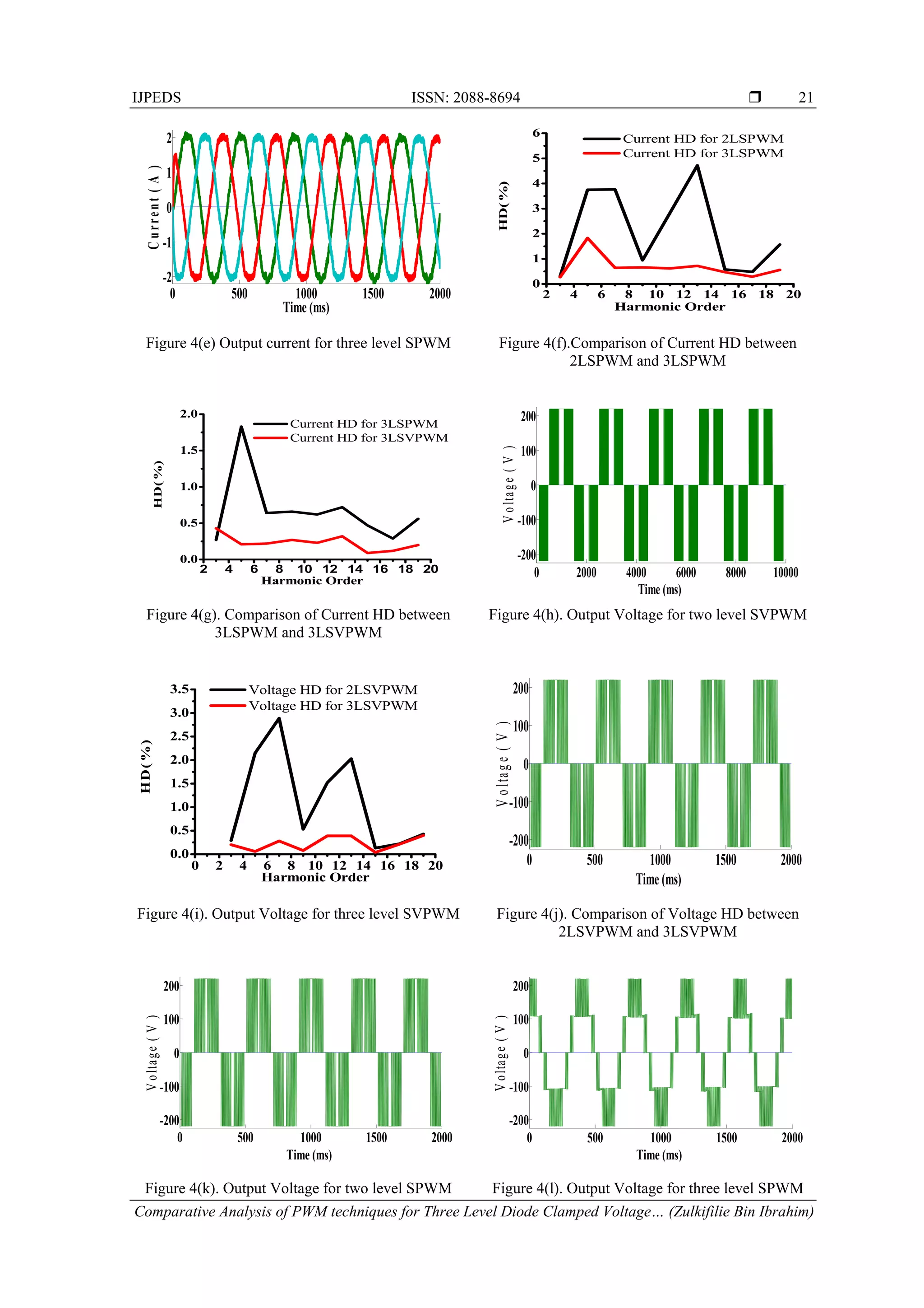
22
Figure 4(m). Comparison of Voltage HD between
2LSPWM and 3LSPWM
Figure 4(n). Comparison of Voltage HD between
3LSPWM and 3LSVPWM
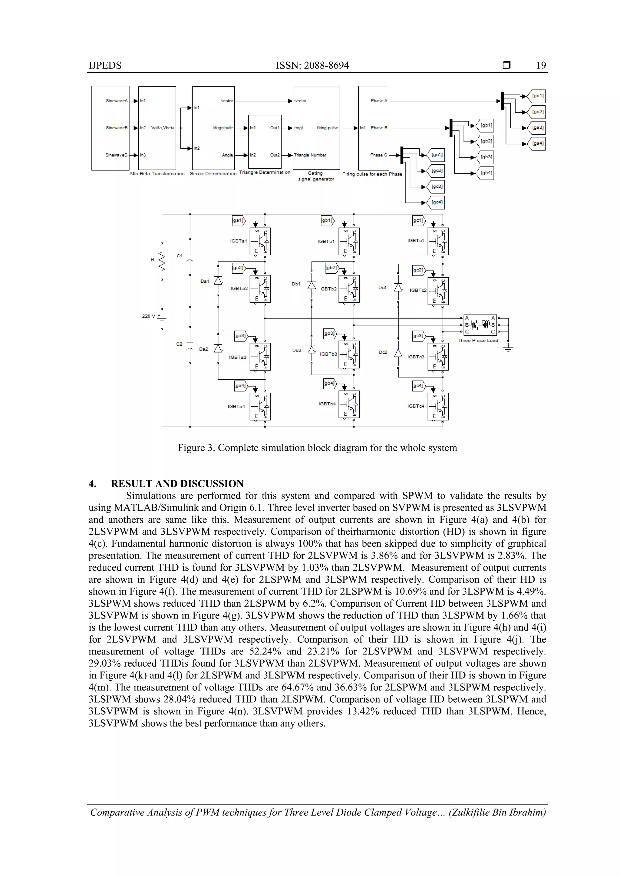
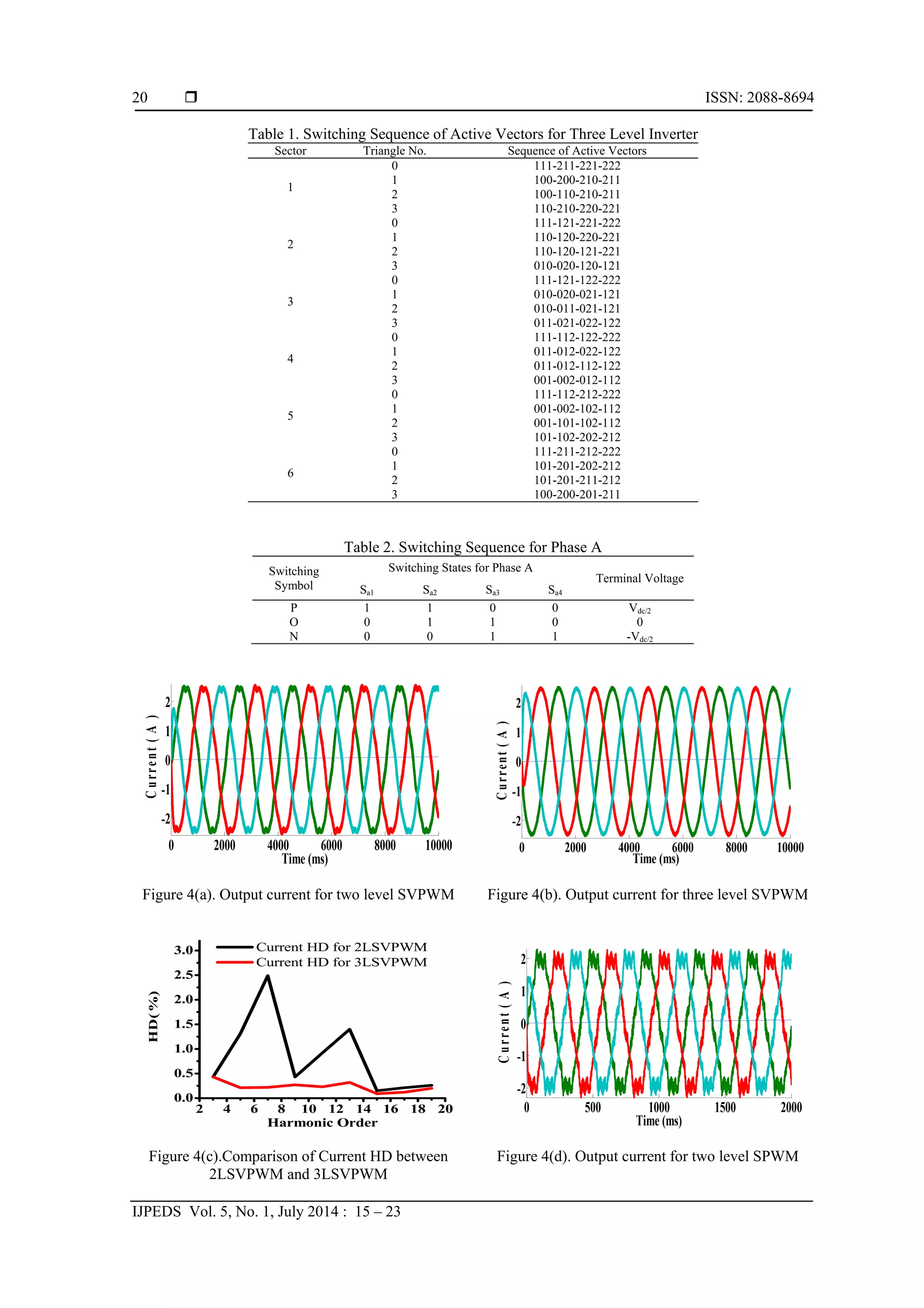
5. CONCLUSION
This paper represents diode clamped three level inverter based on space vector pulse width
modulation and analyzed in details.Simulations are performed with reduced number of switching states (four
active switching states)this system and compared with SPWM to validate the results by using
MATLAB/Simulink and Origin 6.1. From the simulation results, 2LSVPWM shows better performance than
2LSPWM. Furthermore, 3LSVPWM shows better performance than both 2LSVPWM and 3LSPWM in terms
of THD. Hence, it can be concluded that 3LSVPWM gives enhanced fundamental output with better quality
i.e. lesser THD compared to the others.
ACKNOWLEDGEMENTS
This work has been supported by Malaysian Technical Universities Network (MTUN) grant. We
would like to thank all the research students of the Research Laboratory of Electric Vehicle and Drive in
UTeM for their help in solving many critical problems.
REFERENCES
[1] Jose Rodriguez, Steffen Bernet, Peter K Steimer, Ignacio E Lizama. A Survey on Neutral-Point-Clamped Inverters.
IEEE Transactions on Industrial Electronics. 2010; 57(7).
[2] José Rodríguez, Jih-Sheng Lai, Fang ZhengPeng. Multilevel Inverters: A Survey of Topologies, Controls, and
Applications. IEEE Transactions on Industrial Electronics. 2002; 49(4).
[3] Colak, Ilhami, Kabalci, Ersan, Bayindir, Ramazan. Review of multilevel voltage source inverter topologies and
control schemes. Energy Conversion and Management. 2011; 52(2): 795-1574.
[4] Amit Kumar Gupta, Ashwin M Khambadkone. A General Space Vector PWM Algorithm for Multilevel Inverters,
Including Operation in Overmodulation Range. IEEE International Conference on Electric Machines and Drives.
2005: 1437-1444.
[5] Saravanan M, Nandakumar R, Veerabalaji G. Effectual SVPWM Techniques and Implementation of FPGA Based
Induction Motor Drive. International Journal of Reconfigurable and Embedded Systems. 2012; 1(1): 11-18.
[6] Amit Kumar Gupta, Ashwin M Khambadkone. A Space Vector PWM Scheme for Multilevel Inverters Based on
Two-Level Space Vector PWM. IEEE Transactions on Industrial Electronics. 2006; 53(5).
[7] Nikola Celanovic, DushanBoroyevich. A Fast Space-Vector Modulation Algorithm for Multilevel Three-Phase
Converters. IEEE Transactions on Industry Applications. 2001; 37(2).
[8] Poh Chiang Loh, Donald Grahame Holmes. Flux Modulation for Multilevel Inverters. IEEE Transactions on
Industry Applications. 2002; 38(5).
[9] Haoran Zhang, Annette von Jouanne, Shaoan Dai. Multilevel Inverter Modulation Schemes to Eliminate Common-
Mode Voltages. IEEE Transactions on Industry Applications. 2000; 36(6).
[10] JH Seo, CH Choi, DS Hyun. A new simplified space-vector pwm method for three-level inverters. IEEE Trans.
Power Electron. 2001; 16(4): 545-550.
[11] M Trabelsi, L Ben-Brahim, T Yokoyama, A Kawamura, R Kurosawa, T Yoshino. An Improved SVPWM Method
for Multilevel Inverters. 15th International Power Electronics and Motion Control Conference. 2012: LS5c.1-1 -
LS5c.1-7.
[12] Shantanu Chatterjee. A Multilevel Inverter Based on SVPWM Technique for Photovoltaic Application.
International Journal of Power Electronics and Drive System. 2013; 3(1): 62-73.
2 4 6 8 10 12 14 16 18 20
0
1
2
3
4
5
6
7
8
9
HD(%)
Harmonic Order
Voltage HD for 2LSPWM
Voltage HD for 3LSPWM
2 4 6 8 10 12 14 16 18 20
0.0
0.5
1.0
1.5
2.0
2.5
3.0
HD(%)
Harmonic Order
Voltage HD for 3LSPWM
Voltage HD for 3LSVPWM](https://image.slidesharecdn.com/0222may14id6038comparativeanalysisofpwmedit-171213054032/75/Comparative-Analysis-of-PWM-Techniques-for-Three-Level-Diode-Clamped-Voltage-Source-Inverter-8-2048.jpg)
![IJPEDS ISSN: 2088-8694
Comparative Analysis of PWM techniques for Three Level Diode Clamped Voltage… (Zulkifilie Bin Ibrahim)
23
[13] Nupur Mittal, Bindeshwar Singh, SP Singh, Rahul Dixit, Dasharath Kumar. Multilevel Inverters: A Literature
Survey on Topologies and Control Strategies. 2nd International Conference on Power, Control and Embedded
Systems. 2012: 1 – 11.
[14] M ValanRajkumar, PS Manoharan. FPGA based multilevel cascaded inverters with SVPWM algorithm for
photovoltaic system. Solar Energy. 2013; 87: 229–245.
[15] Amit Kumar Gupta, Ashwin M Khambadkone. A General Space Vector PWM Algorithm for Multilevel Inverters,
Including Operation in Overmodulation Range. IEEE Transactions on Power Electronics. 2007; 22(2).
[16] Lin Lei, ZhongHeqing, Deng Yu, Zhang Jie, ZouYunping, She Xu. A DTC Algorithm for Three-level Induction
Motor Drives System Based on Discrete Space Vector Modulation. Twenty-Fourth Annual IEEE Applied Power
Electronics Conference and Exposition. 2009: 1978-1983.](https://image.slidesharecdn.com/0222may14id6038comparativeanalysisofpwmedit-171213054032/75/Comparative-Analysis-of-PWM-Techniques-for-Three-Level-Diode-Clamped-Voltage-Source-Inverter-9-2048.jpg)


![[9_CV] FCS-Model Predictive Control of Induction Motors feed by MultilLevel C...](https://cdn.slidesharecdn.com/ss_thumbnails/9cvfcs-modelpredictivecontrolofinductionmotorsfeedbymultillevelcasadedh-bridgeinverter-190418083950-thumbnail.jpg?width=640&height=640&fit=bounds)