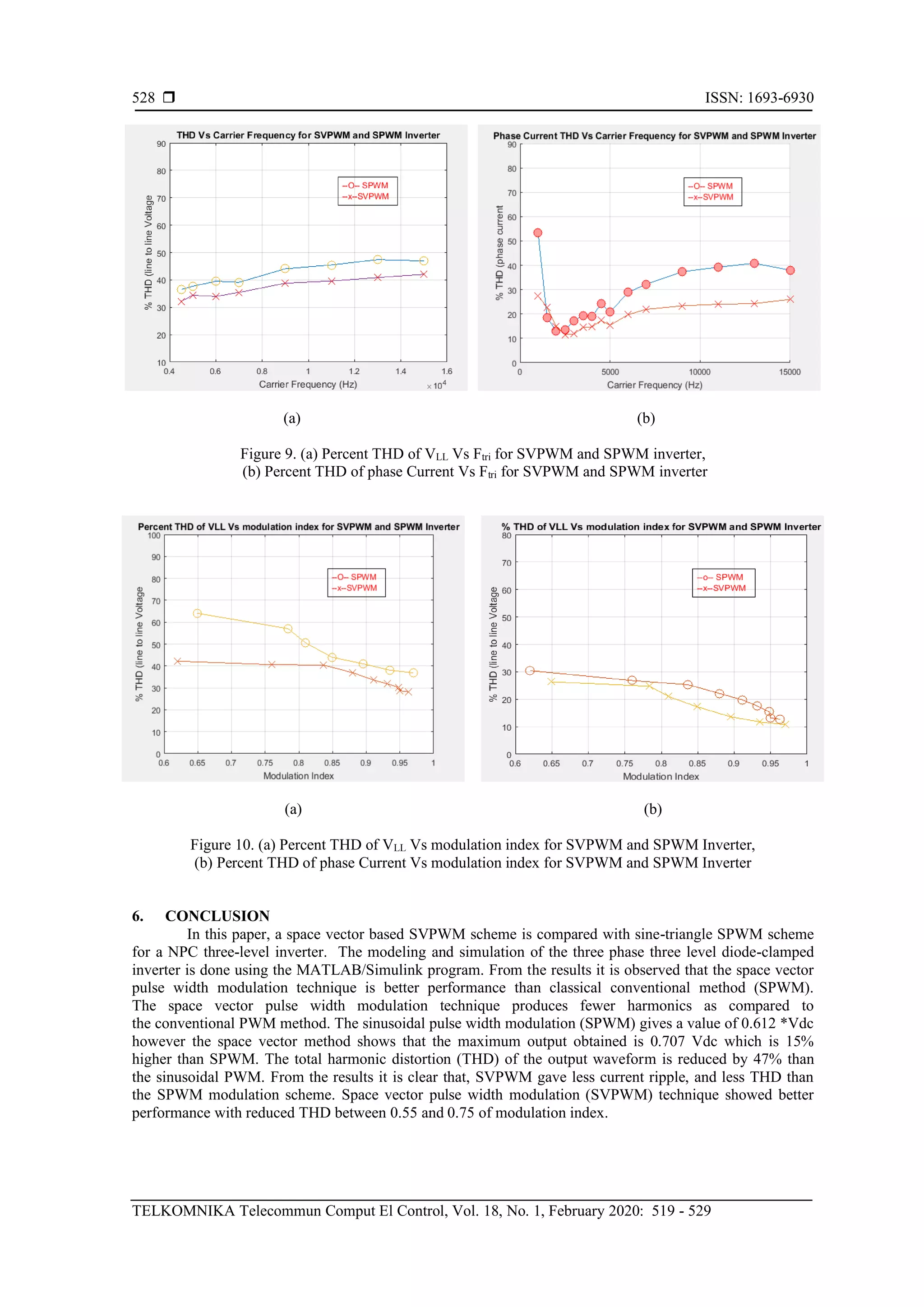
This document discusses two pulse width modulation (PWM) techniques for three-phase three-level inverter drives, focusing on sinusoidal PWM and space vector PWM. It introduces the three-level neutral-point clamped inverter structure and demonstrates the advantages of space vector PWM over traditional methods in terms of voltage utilization, current ripple reduction, and harmonic performance. The paper also details a mathematical formulation for the switching sequence and includes a comprehensive comparative analysis of simulation results.
![TELKOMNIKA Telecommunication, Computing, Electronics and Control
Vol. 18, No. 1, February 2020, pp. 519~529
ISSN: 1693-6930, accredited First Grade by Kemenristekdikti, Decree No: 21/E/KPT/2018
DOI: 10.12928/TELKOMNIKA.v18i1.12440 519
Journal homepage: http://journal.uad.ac.id/index.php/TELKOMNIKA
PWM control techniques for three phase three level
inverter drives
Arkan A. Kadum
Department of Electrical Engineering, University of Kufa, Iraq
Article Info ABSTRACT
Article history:
Received Jan 26, 2019
Revised Jun 2, 2019
Accepted Jul 18, 2019
In this paper two very efficient pulse width modulation techniques were
discussed named Sin pulse width modulation and space vector pulse width
modulation. The basic structure of the three-level inverter neutral-point
clamped is introduced and the basic idea about space vector pulse width
modulation for three-level voltage source inverter has been discussed in
detail. Nearest three vectors space vector pulse width modulation control
algorithm is adopted as the control strategy for the three phase three level
NPC inverter in order to compensate the neutral-point shifting. Mathematical
formulation for calculating switching sequence has determined. Comparative
analysis proving superiority of the space vector pulse width modulation
technique over the conventional pulse width modulation, and the results of
the simulations of inverter confirm the feasibility and advantage of the space
vector pulse width modulation strategy over sin pulse width modulation in
terms of good utilization of dc-bus voltage, low current ripple and reduced
switching frequency. Space vector pulse width modulation provides
advantages better fundamental output voltage and useful in improving
harmonic performance and reducing total harmonic distortion.
Keywords:
Multi-level converters
Neutral-point-clamped inverter
Space vector pulse width
modulation
Three-level inverter
This is an open access article under the CC BY-SA license.
Corresponding Author:
Arkan A. Kadum,
Department of Electrical Engineering,
University of Kufa, Iraq.
Email: arkana.doabel@uofkufa.edu.iq
1. INTRODUCTION
Multilevel inverter topologies [1, 2] have got special attention during the earlier two decades due to
their significant advantages compared to the classical two level inverters. As compared with two-level
inverters, multilevel inverters have multiple advantages, for example, low harmonics in output voltages and
current, less dv/dt, lower power losses across switching devices, less common mode voltages, and higher
quality output waveform [3-7]. Therefore a new family of multilevel inverters has emerged as the solution for
different applications; such as, AC power supplies, large powerful engine drivers, transmission, distribution
systems and medium voltage grid [8-12].
Different types of topologies of power conversion have been proposed with the aim of improving
the total harmonic distortion (THD) and efficiency, and reducing the complexity of control. The most known
are: cascaded H-bridge (CHB) inverter, flying-capacitors (FC) converter, packed U cells, [13-16] and neutral
point clamped (NPC) inverter [1]. This paper uses the NPC topology because it has the advantages such as:
low switching frequency, DC-link capacitors are common to three phases and reactive current can be
controlled [14]. The diode-clamped three level neutral-point clamped (NPC) topology has been the most](https://image.slidesharecdn.com/5812440-200715060502/75/PWM-control-techniques-for-three-phase-three-level-inverter-drives-1-2048.jpg)
![ ISSN: 1693-6930
TELKOMNIKA Telecommun Comput El Control, Vol. 18, No. 1, February 2020: 519 - 529
520
widely used one among all multilevel inverter topologies due to their use of a unique DC source of voltage
compared with the CHB inverters and higher performance when compared to the FL inverters [17, 18].
On the other hand, several methods of modulation techniques have been proposed for this type of
converter. The most known techniques are: selective harmonic elimination pulse width modulation (PWM),
sinusoidal PWM with and without harmonic injection, space vector modulation, sigma delta PWM, and
closed loop modulation techniques exist to control the inverter [19-22]. Among the possible multilevel
topologies, the sine triangle PWM (SPWM) and space vector PWM (SVPWM) are probably the most popular
modes and the most common PWM generation techniques for three-level three-phase multilevel inverters.
The SVPWM is basically divided into two classifications: the nearest three vectors (NTV) method and
the Hexagons method. The SVPWM includes the reference voltage space vector synthesis for the NTV
approach, by switching between the nearest three voltage space vectors [23-26]. The output voltage vector is
synthesized for the hexagon's approach using a method similar to the traditional two-level converter.
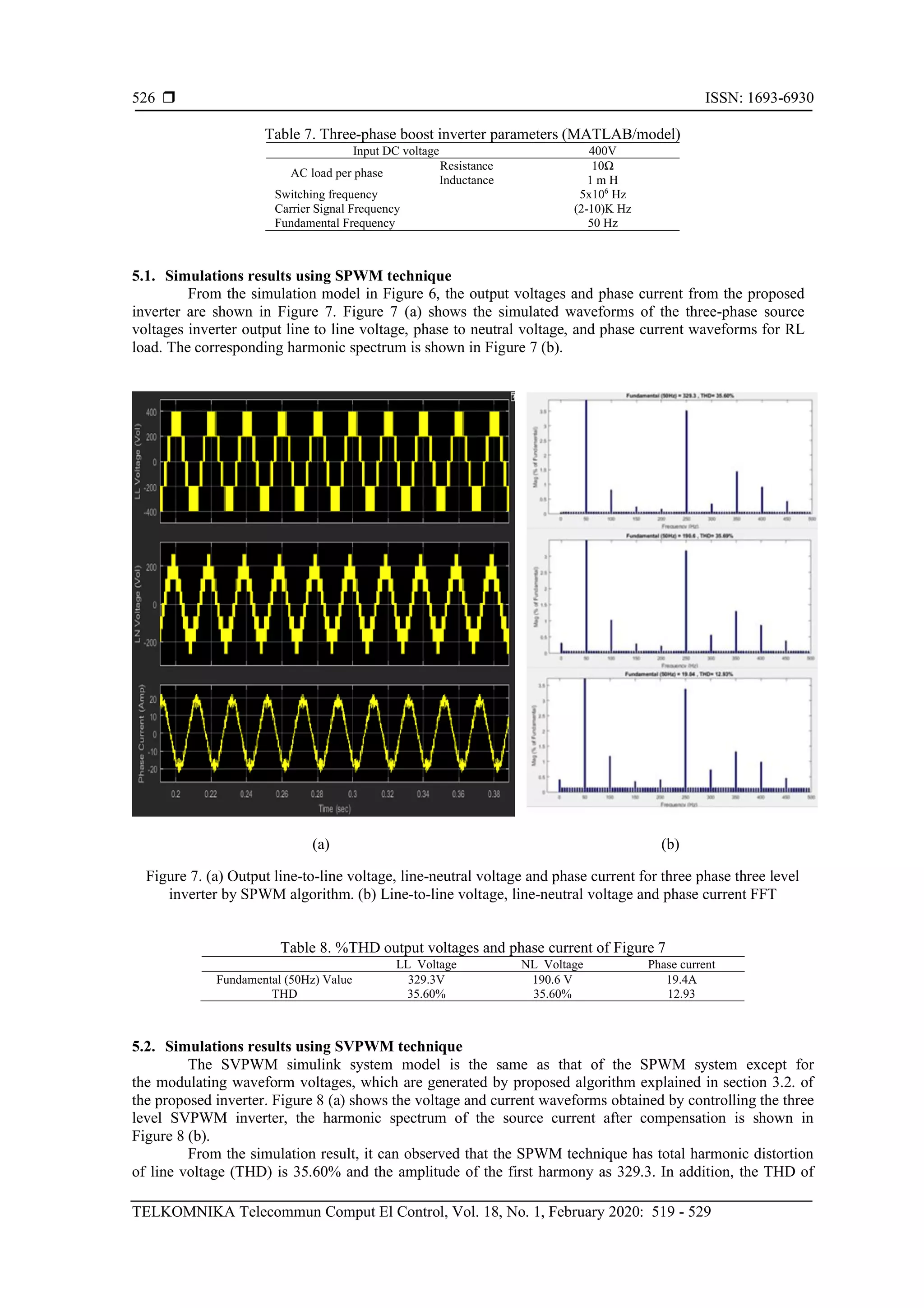
This paper modeling and simulation of a three-level NPC inverter have been performed with SPWM
and SVPWM techniques using MATLAB/Simulink software. The results of the comprehensive comparison
are presented in two ways. This paper will be divided into six sections. A brief review of the three level NPC
inverter is provided in section 2. Sections 3 describes the three level PWM techniques. The proposed
three-level space voltage vector algorithm has given in section 4. Section 5 will perform the simulation
successively. Finally, at the end of this paper, a general conclusion is given.
2. THREE-LEVEL DIODE-CLAMPED INVERTER TOPOLOGY
Figure 1 shows the three-phase three-level diode-clamped inverter (NPC) topology. From Figure 1,
each phase of the inverter shared the DC-link supply. The center of each phase is connected to the common
point of the series capacitors. The inverter is feeding an AC a three-phase load. Three-level output consisting
of levels -Vdc, 0, + Vdc depending on the DC-bus voltage. Table 1 shows the functioning principle. In order
to obtain the desired three-level voltages, the converter must ensure complementarities between the pairs of
switches: (Si1,Si4) and (Si2,Si3) where 'i' is the phase indicator (i = a, b, c), Vio is the phase-to-fictive middle
point voltage. Table 1 shows switching of the i-phase in Figure 1 with switching states and corresponding
output voltage levels.
Figure 1. Three-phase three-level NPC inverter circuit
Table 1. Relationship between switching devices and output level
Switching Situations
i-phase of NPC inverter
Terminal Voltage
Si1 Si2 Si3 Si4
P 1 1 0 0 +Vdc /2
O 0 1 1 0 0
N 0 0 1 1 -Vdc /2
3. THREE-LEVEL PWM TECHNIQUES
In many applications, the output voltage of the inverter is often required to vary due to
the following reasons:](https://image.slidesharecdn.com/5812440-200715060502/75/PWM-control-techniques-for-three-phase-three-level-inverter-drives-2-2048.jpg)
![TELKOMNIKA Telecommun Comput El Control
PWM control techniques for three phase three level inverter drives (Arkan A. Kadum)
521
− To compensate the input voltage variations.
− To compensate for the regulation of the inverters.
− For the provision of special loads that will need variation of voltage with frequency.
3.1. Sinusoidal pulse width modulation technique
The principle of the sinusoidal carrier-based pulse width modulation (SPWM) technique;
a high-frequency triangular carrier wave Vr is compared with a sinusoidal control signal Vc at the desired
frequency. The intersection of Vc and Vr waves determines the switching instants and commutation of
the modulated pulse. A transition in PWM waveform is generated at each compare match point. When
sinusoidal wave has magnitude higher than the triangular wave the PWM output is positive and when Vc is
smaller than Vr, the output is negative. The inverter’s switching frequency fs establishes by the frequency of
triangle waveform Vc. The fundamental frequency component in the inverter output voltage can be
controlled by amplitude modulation index; we define the modulation index mi as follows:
mi = Vc / Vr (1)
where Vc and Vr are the peak values of the modulating and carrier waves, respectively. The amplitude
modulation index mi is usually adjusted by varying Vc while keeping Vr fixed. The frequency modulation
index is defined by:
mf = fr / f1 (2)
where, f1 and fr are the frequencies of the modulating and carrier waves, respectively. The fundamental
component Vout1 of the output voltage has the property as depicted in equation below in a linear
modulation region:
Vout1 = mi * Vd mi ≤ 1.0 (3)
in (1) shows that the modulation index and amplitude of the fundamental component of
the output voltage varies linearly. The mi value varied from zero to one; it is defined as the linear control
range of sinusoidal carrier PWM. Three level pulse width modulated waveforms can be generated by sine
carrier PWM. Sine carrier PWM is generated by comparing the three reference control signals with two
triangular carrier waves [6, 12].
The three-level sine-PWM inverter is implementation as a two-level inverter using the same
principle. Here sine carrier PWM is generated by comparing the three reference control signals with two
triangular carrier waves. The corresponding pulses are generated which are to be supplied to the inverter gate
devices. The three reference control signals are phase shift by an angle 2π/3 and 4π/3 with same amplitude.
Two carrier waves are in phase each other with dc voltage offset. For three-phase SPWM;
𝑉𝑝𝑒𝑎𝑐𝑘 = 𝑚
𝑣 𝑑𝑐
2
(4)
where: Vpeak is the peak value of the fundamental component of the phase-to-neutral voltage, vdc is the DC
link voltage. For three-phase space-vector SVPWM, [13].
𝑉𝑝𝑒𝑎𝑐𝑘 = 𝑚
𝑣 𝑑𝑐
√3
(5)
For normal steady-state operation, 0 <m ≤ 1.
3.2. Space vector pulse width modulation
The basic principle of SVPWM depends on synthesizing the vector of reference voltage by time
averaging of the two vectors produced by the inverter. The reference voltage vector is the required command
voltage which that should be given as required to the application. Space vector PWM technique is based on
rotating reference voltage space vector approximation. The rotating reference voltage vector represents
the spatial vector sum of the three-phase voltage in the α-β space. The amplitude of the vector and the phase
angle of the three-phase can be determined by the instantaneous values of the voltages. If the magnitudes are
sinusoidal and balanced, the vector it will rotate rapidly in a fixed angular and have a constant amplitude.
When considering the three phase of the inverter, there are 27 switching state. Each of these switching states
can be represented as a vector using (6):](https://image.slidesharecdn.com/5812440-200715060502/75/PWM-control-techniques-for-three-phase-three-level-inverter-drives-3-2048.jpg)
![ ISSN: 1693-6930
TELKOMNIKA Telecommun Comput El Control, Vol. 18, No. 1, February 2020: 519 - 529
522
𝑉
→
= 𝑉𝛼 + 𝑗𝑉𝛽 =
2
3
(𝑉𝑎 𝑒 𝑗0
+ 𝑉𝑏 𝑒
𝑗2𝜋
3 + 𝑉𝑐 𝑒
𝑗4𝜋
3 ) (6)
𝜽 = 𝒕𝒂𝒏−𝟏
(
𝑽 𝜶
𝑽 𝜷
) (7)
where Va, Vb, Vc are the reference three-phase voltages and Vα and Vβ are the components of reference vector
in α-β coordinate system. Through the use Clark transformation, the a-b-c three-phase coordinate system is
transformed to 2-dimentional α-β frame that is helpful in sector identification by following expression:
[
𝑉𝛼
𝑉𝛽
] =
2
3
[
1 −
1
2
−
1
2
0
√3
2
−
√3
2
] [
𝑉𝑎
𝑉 𝑏
𝑉 𝑐
] (8)
The 27 output voltage vectors in the three-level VSI as shown in Figure 2. The space-vector diagram
shown in Figure 2 consists of 6 major triangular sectors. Each major section represents π/3 of
the fundamental cycle. There are 4 minor triangular sectors within each major sector. Therefore, the total is
24 minor sectors in the plane. The voltage vector is represented by the vertices of these sectors. Based on
the amplitude the three-level inverter vectors are divided into large, medium, small, and zero vectors, they are
listed as shown in Table 2.
As can be seen in Figure 2, the voltage vectors are located at the various points of the two hexagons
interleaved according to their switching. The voltage vectors of group large voltage vectors, with amplitudes
of 2Vdc/3 and located at the corners of the outer hexagon. The medium voltage vector is the voltage vector of
amplitude Vdc/√3 and is located at the midpoint of the outer hexagon. Small group voltage vectors with
amplitudes of Vdc/3 and are located at the corners of the inner hexagon. When the rotating voltage vector falls
into a certain sector in a three-phase three-level inverter, adjacent voltage vectors are selected to synthesize
the desired rotating voltage vector based on the principle of vector synthesis, resulting in PWM waveforms in
three-phase. The sector in which Vo* resides can be examined by examining the phase angle and
the magnitude of a rotating reference voltage vector V*.
Figure 2. Space voltage vectors in three-level inverter
Table 2. Voltage vectors and switching states
Vector name vector classification
Zero vector [OOO] [PPP] [NNN]
Small vector
P-type N-type
[PPO] [POO] [ONN] [ONN]
[OPP] [OPO] [NOO] [NNO]
[POP] [OOP] [ONO] [NON
Medium vector [NPO] [PON] [OPN]
[PNO] [ONP] [NOP]
Large vector [PPN] [PNN] [NPN]
[PNP] [NNP] [NPP]](https://image.slidesharecdn.com/5812440-200715060502/75/PWM-control-techniques-for-three-phase-three-level-inverter-drives-4-2048.jpg)
![TELKOMNIKA Telecommun Comput El Control
PWM control techniques for three phase three level inverter drives (Arkan A. Kadum)
523
4. THREE-LEVEL INVERTERS SPACE VOLTAGE VECTOR ALGORITHM
As shown in Figure 3, the primary task of SVPWM is to determine, which sector and which of
the region, then determine the corresponding output space voltage vectors. The realization of the voltage
vector SVPWM is subsumed into the proposed SVPWM technique following steps:
− Transformation of 3-phase to 2-phase.
− Determining the sector containing the tip of the reference vector.
− Determine the region in the corresponding sector.
− Deduction of optimum switching sequence.
− Generation of gating signals to the inverter devices.
− Calculating the duration of switching vectors.
Step 1: Using park’s transformation to calculate Vα, Vβ, Vref and the angle (θ) (8).
Step 2: After calculating θ, determine the sector according to Vref position of as shown in Table 3
Step 3: Determine the region in the corresponding sector. The reference voltage vector can be found in space
vector diagram in any region (1-4) of any sector (1-6) as shown in Figure 2.
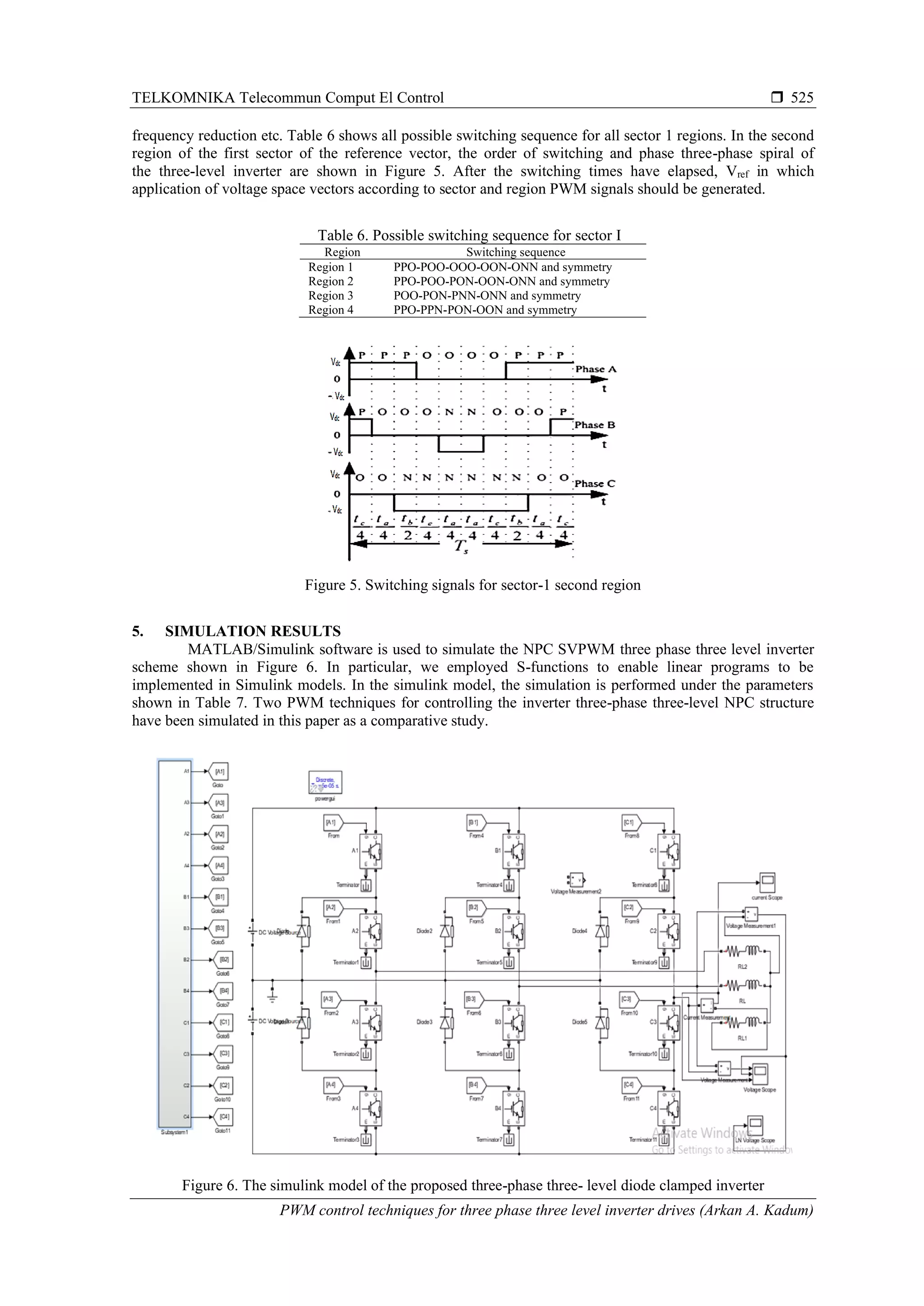
To estimate the region in sector 1, space vector diagram for m1 and m2 is shown in Figure 3, and
corresponding switching logic is given in Table 4.
(a) (b)
Figure 3. Space vector diagram for m1 and m2 in sector 1
Table 3. Sector calculation based on the location of Vref
Range of 𝛼
(degree)
0 ≤ 𝜃 < 60 60 ≤ 𝜃 < 120 120 ≤ 𝜃 < 180 180 ≤ 𝜃 < 240 240 ≤ 𝜃 < 300 300 ≤ 𝜃 < 360
Location of Vref Sector I Sector II Sector III Sector IV Sector V Sector VI
𝑚1 = 𝑑 − 𝑐 = 𝑚𝑐𝑜𝑠𝜃 − (
2
√3
𝑚𝑠𝑖𝑛𝜃) cos (
𝜋
3
)
= 𝑚 (𝑐𝑜𝑠𝜃 −
𝑠𝑖𝑛𝜃
√3
) = 𝑚
2
√3
𝑠𝑖𝑛 (
𝜋
3
− 𝜃) (9)
𝑚2 = 𝑎 =
𝑏
sin (𝜋/3)
=
2
√3
𝑚𝑠𝑖𝑛𝜃 (10)
𝑚 =
𝑉 𝑟𝑒𝑓
2𝑉 𝑑𝑐/3
(11)
Table 4. Logic used to find the region in which Vref is located
X1 and X2 Position of Vref
X1, X2 and (X1 + X2) < 0.5 Region 1
X2 > 0.5 Region 2
X1 > 0.5 Region 3
X1 and X2 < 0.5 and (X1 + X2) > 0.5 Region 4
Step 4: Calculation of switching time. Determine the switching time of each switch across all the regions.
The SVPWM technique for three-level inverters is called "voltage-time equalization”
principle [10]. For example, considering that the reference vector Vref is locating in sector I and in region 2,
for this region, the nearest three voltage space vectors are V1, V7 and V2 are shown in Figure 4.
Once the nearest three vectors have been identified, by using the volt-second balance method, the on-time
calculations of the corresponding vectors can be developed as the following expressions. When the voltage in
the second sector is equal to the time synchronization equation; can be written as in (12).](https://image.slidesharecdn.com/5812440-200715060502/75/PWM-control-techniques-for-three-phase-three-level-inverter-drives-5-2048.jpg)
![ ISSN: 1693-6930
TELKOMNIKA Telecommun Comput El Control, Vol. 18, No. 1, February 2020: 519 - 529
524
𝑣 𝑟𝑒𝑓 𝑇𝑠 = 𝑣1 𝑡 𝑎 + 𝑣7 𝑡 𝑏 + 𝑣2 𝑡 𝑐 (12)
𝑇𝑠 = 𝑡 𝑎 + 𝑡 𝑏 + 𝑡 𝑐
where Ts is the sampling time, ta, tb and tc are switching on-times for the V1, V 7 and V 2 vectors respectively.
𝑉1 =
𝑉 𝑑𝑐
3
𝑒 𝑗0
𝑉2 =
𝑉 𝑑𝑐
3
𝑒 𝑗𝜋/3
=
𝑉 𝑟𝑒𝑓
2
3
𝑉 𝑑𝑐
𝑒 𝑗𝜃
𝑇𝑠 =
1
2
𝑡 𝑎 +
√3
2
𝑒 𝑗
√3
6 𝑡 𝑏 +
1
2
𝑒 𝑗
√3
3 𝑡 𝑐
𝑉7 =
𝑉 𝑑𝑐
√3
𝑒 𝑗𝜋/6
By solving the 3 equations above, the on-time of the concerned vectors can be computed by [14]:
𝑡 𝑎 = 𝑇𝑠 − 2𝑘𝑠𝑖𝑛𝜃
𝑡 𝑏 = 2𝑘𝑠𝑖𝑛(
𝜋
3
+ 𝜃) − 𝑇𝑠
𝑡 𝑐 = 𝑇𝑠 − 2𝑘𝑠𝑖𝑛 (
𝜋
3
− 𝜃)
𝑘 =
2
√3
𝑚𝑇𝑠
where, Ts is the system sampling control cycle, and Vref, θ is the amplitude and angle of the reference
voltage vector.
Figure 4. Synthesized reference vector in the first sector
The on-times for other regions in the first sector equilibrium time equations can be computed by using
similar procedure as expressed in Table 5. These equations can be made valid for other space vector
diagram within the sectors [18].
Table 5. Equations of switching times for sector-1
region
On time
ta tb tc
1 2𝑘𝑠𝑖𝑛(
𝜋
3
− 𝜃) 𝑇𝑠 − 2𝑘𝑠𝑖𝑛(
𝜋
3
+ 𝜃) 2𝑘𝑠𝑖𝑛𝜃
2 𝑇𝑠 − 2𝑘𝑠𝑖𝑛𝜃 2𝑘𝑠𝑖𝑛 (
𝜋
3
+ 𝜃) − 𝑇𝑠 𝑇𝑠 − 2𝑘𝑠𝑖𝑛(
𝜋
3
− 𝜃)
3 2𝑘𝑠𝑖𝑛𝜃 − 𝑇𝑠 2𝑘𝑠𝑖𝑛(
𝜋
3
− 𝜃) 2𝑇𝑠 − 2𝑘𝑠𝑖𝑛(
𝜋
3
+ 𝜃)
4 2𝑇𝑠 − 2𝑘𝑠𝑖𝑛(
𝜋
3
+ 𝜃) 2𝑘𝑠𝑖𝑛𝜃 2𝑘𝑠𝑖𝑛 (
𝜋
3
− 𝜃) − 𝑇𝑠
Step 5: Inverter's gating signals generation
The next step in implementation of SVPWM is the selection of the redundant states optimal
switching sequence of which is useful in balancing of DC link voltages, fault tolerance and switching](https://image.slidesharecdn.com/5812440-200715060502/75/PWM-control-techniques-for-three-phase-three-level-inverter-drives-6-2048.jpg)

![TELKOMNIKA Telecommun Comput El Control
PWM control techniques for three phase three level inverter drives (Arkan A. Kadum)
529
REFERENCES
[1] J. Rodríguez, et al., “Multilevel inverters: a survey of topologies, controls and applications,” IEEE Trans. Ind.
Electron., vol. 49, no. 4, pp. 724-738, Aug 2002.
[2] M. Chen and D. Sun, “A Unified Space Vector Pulse Width Modulation for Dual Two-level Inverter System,”
IEEE Transactions on Power Electronics, vol. 32, no. 2, pp. 889-893, Feb 2017.
[3] T. E. Sults, et al., “Novel Space Vector Pulsewidth Modulation Strategies for Single-Phase Three-Level NPC
Impedance-Source Inverters,” IEEE Transactions on Power Electronics, vol. 34, no. 5, May 2019.
[4] C. Hu, et al., “An Improved Virtual Space Vector Modulation Scheme for Three-Level Active Neutral-Point-
Clamped Inverter,” IEEE Transactions on Power Electronics, vol. 32, no. 10, pp. 7419-7434, Oct 2017.
[5] L. Demas, et al., “Comparative study of multilevel topologies: NPC, multicell inverter and SMC with IGBT,” in
Proc. IEEE Industrial Electronics Soc. Conf., 2002.
[6] A. Nabae, et al., “A new neutral-point clamped PWM inverter,” IEEE Trans. Ind. Applicat., vol. IA-17, no. 5,
pp. 518-523, Sept/Oct 1981.
[7] K. Zhou and D. Wang, “Relationship between space-vector modulation and three-phase carrier-based PWM: A
comprehensive analysis,” IEEE Trans. Ind. Electron., vol. 49, pp. 186-196, Feb 2002.
[8] J. H. Seo, et al., “A new simplified space-vector PWM method for three-level inverters,” IEEE Trans. Power
Electron., vol. 16, pp. 545-550, Jul 2001.
[9] B. Belkacem, et al., “A Comparative Study Between the Nearest Three Vectors and Two-Level Hexagons Based
Space Vector Modulation Algorithms for Three-Level NPC Inverters,” Journal of Power Technologies, vol. 97,
no. 3, pp. 190-200, 2017.
[10] P. Chamarhi, et al., “Simplified Implementation Scheme for Space Vector Pulse Width Modulation of n-Level
Inverter with Online Computation of Optimal Switching Pulse Durations,” IEEE Transactions on Industrial
Electronics, vol. 63, no. 11, pp. 6695-6704, Nov 2016.
[11] F. Sebally, et al., “Design and Implementation of Space Vector Modulation-Based Sliding Mode Control for
Grid-Connected 3L-NPC Inverter,” IEEE Transactions on Industrial Electronics, vol. 63, no. 12, pp. 7854-7863,
Dec 2016.
[12] S. Bhattacharya, et al., “Space-Vector-Based Generalized Discontinuous Pulsewidth Modulation for Three-Level
Inverters Operating at Lower Modulation Indices,” IEEE Journal of Emerging and Selected Topics in Power
Electronics, vol. 5, no. 2, pp. 912-924, Jun 2017.
[13] I. O. Charles, “A Cascaded Multi-level Inverter Topology with Improved Modulation Scheme,” Electric Power
Components and Systems, vol. 42, no. 7, pp. 768-777, 2014.
[14] S. Sezen and E. Ozdemir, “Modeling, simulation and control of three-phase three level multilevel inverter for grid
connected photovoltaic system,” vol. 15, no. (3-4), pp. 335-341, Mar/Apr 2013.
[15] R. Attia, et al., “Space Vector Pulse Width Modulation for Three Phase Cascaded H-Bridge Inverter,” IEEE: 2018
International Conference on Applied Smart Systems (ICASS), Nov 2018.
[16] H. Vahedi, et al., “Balancing three-level neutral point clamped inverter DC bus using closed-loop space vector
modulation: real-time implementation and investigation,” vol. 9, no. 10, pp. 2076-2084, Aug 2016.
[17] M. D. Manjrekar, et al., “Hybrid multilevel power conversion system: a competitive solution for high-power
applications,” Conference Record of the 1999 IEEE Industry Applications Conference, 1999.
[18] M. Rajesh and B. Singh, “Three-level NPC rectifier-based midpoint converter-fed SRM drive,” Int. J. Power
Electronics, vol. 6, no. 1, pp.1-17, 2014.
[19] V. Oleschuk, et al., “Six-phase vehicular drive with renewable dc sources and hybrid PWM control of four
inverters,” 2015 International Conference on Renewable Energy Research and Applications (ICRERA), 2015.
[20] C. Bharatiraja, et al., “A common-mode leakage current mitigation for PV-grid connected three-phase three-level
transformerless T-type-NPC-MLI,” 2016 IEEE International Conference on Renewable Energy Research and
Applications (ICRERA), Birmingham, 2016.
[21] H. Chen and H. Zhao, “Review on pulse-width modulation strategies for common-mode voltage reduction in three-
phase voltage-source inverters,” vol. 9, no. 14, pp. 2611-2620, Nov 2016.
[22] A. A. Yacine, et al., “Implementation of Modified SVPWM for Three-level Inverter Using STM32F4,” IEEE 2018
International Conference on Electrical Sciences and Technologies in Maghreb (CISTEM), Algiers, Algeria, 2018.
[23] F. Z. Lahouar, et al., “DSP based real-time implementation of a space vector modulation scheme for three-phase
three-level NPC converter,” International Renewable Energy Congress (IREC 2015), Mar 2015.
[24] G. C. Chen, “PWM Inverse Technology and Applica-tion,” Beijing, Electric Power Publication, 2007.
[25] I. Ahmed, et al., “Simplified Space Vector Modulation Techniques for Multilevel Inverters,” IEEE Transactions on
Power Electronics, vol. 31, no. 12, pp. 8483-8499, Dec 2016.
[26] Duc-Tri Do, et. al., “Space Vector Modulation Strategy for Three-Level Quasi-Switched Boost T-Type Inverter,”
2018 IEEE 4th
Southern Power Electronics Conference (SPEC), 2018.](https://image.slidesharecdn.com/5812440-200715060502/75/PWM-control-techniques-for-three-phase-three-level-inverter-drives-11-2048.jpg)