Download to read offline
![RTL Verification and FPGA Implementation of 4x4
Vedic Multiplier
Mohd Esa , Konasagar Achyut and Chandrajeet Singh
Abstract. The objective of this paper is to study 4x4 Vedic multiplier.
Multiplication is an important fundamental function in arithmetic operations.
Vedic multiplier using Urdhva-Tiryagbyam sutra is predominant in
performance evaluation of parameters such as power, area & delay. This paper
presents design, verification and FPGA implementation of Vedic multiplier.
Verification is carried out in Questa Sim 10.4e using System Verilog HVL and
design is carried out in Xilinx ISE Design Suite 14.7 using Verilog HDL
environment.
Keywords: Vedic Multiplier, HVL, HDL, RTL, FPGA.
1 Introduction
inary number system uses only zero‟s and one‟s. Just like decimal system,
binary possesses every arithmetic operation. A binary multiplier is any such
electronic circuit used in digital electronics to multiply two binary numbers
[1]. Unlike the decimal base ten, binary multiplication is done in binary base two. The
concept of Vedic multiplier has been acquired from the Vedic mathematics in which
there are several methods to operate with the number systems.Urdhva-Triyagbhyam
sutra is one among those Vedic methods which helps to follow general formula
applicable to all cases in multiplication. The meaning of Urdhva-Triyagbhyam is
vertically and crosswise.
This paper presents the design and verification of 4x4 bit Vedic multiplier
using HDL and HVL respectively, which helps us to justify that design is working
without any bugs or errors. This paper also presents implementation of Vedic
multiplier in Field Programming Gate Array.FPGAs are semiconductor devices that
are based around a matrix of configurable logic blocks connected via programmable
interconnects. FPGAs can be reprogrammed to desired application or functionality
requirements after manufacturing.
2 Ripple Carry Adder
As the name of the circuit itself represents that the carry is rippled to a
succeeding part. The combination of full adders whose carry output is propagated as a
B
Parishodh Journal
Volume IX , Issue III , March/2020
ISSN NO:2347-6648
Page No:772](https://image.slidesharecdn.com/82-p-march-1066-200321062124/75/RTL-Verification-and-FPGA-Implementation-of-4x4-Vedic-Multiplier-1-2048.jpg)
![carry input to the succeeding full adder is called as a Ripple Carry Adder. The
addition of two binary numbers in parallel implies that all the bits of addend and
augend are available for computation at the same time [2].
Fig.1. Ripple Carry Adder logic circuit
Table 1.Ripple Carry Adder truth table
In this work, three ripple carry adders are used in which the first bits from addend and
augend binary numbers are computed by half adders and rest with full adders to form
a complete ripple addition. The truth table for various possible combinations of ripple
carry adder is shown table 1.
3 Urdhva Triyagbhyam Sutra
Mathematics is mother of all sciences, it is full of mysteries and magic.
Ancient Indians were able to understand these mysteries and developed simple keys
to solve them. The ancient system of Vedic maths was introduced by Swami Bharati
Krishna Tirthaji. His work includes various methods of calculations and this in turn
Indians named it as Vedic mathematics [3].
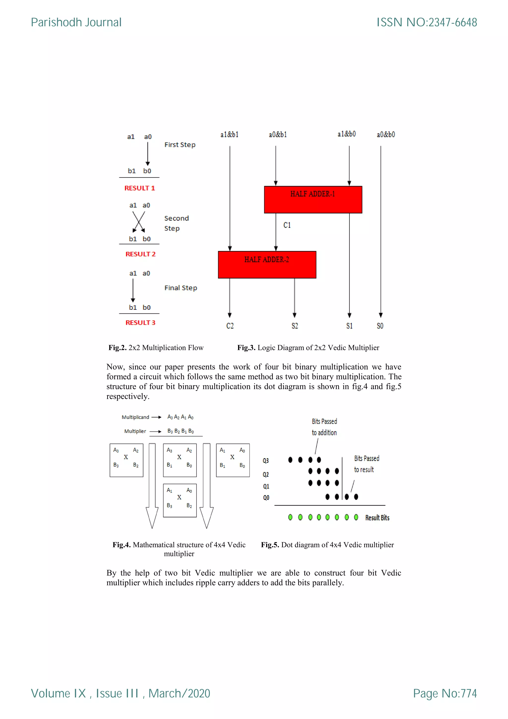
This paper presents multiplication operation done over two 4-bit binary
numbers through the Urdhva-Triyagbhyam technique. As usual the multiplication has
a multiplier and a multiplicand, but the method of multiplication is done by
multiplying first two bits of multiplicand and multiplier followed by cross
multiplication of side numbers of multiplicand with numbers in multiplier, finally the
last digits are multiplied parallelly to complete the multiplication process. This
method can be observed as shown in the fig.2 for two bit binary numbers. To perform
this in digital logic the block diagram of two bit Vedic multiplier is shown in fig.3.
Parishodh Journal
Volume IX , Issue III , March/2020
ISSN NO:2347-6648
Page No:773](https://image.slidesharecdn.com/82-p-march-1066-200321062124/75/RTL-Verification-and-FPGA-Implementation-of-4x4-Vedic-Multiplier-2-2048.jpg)

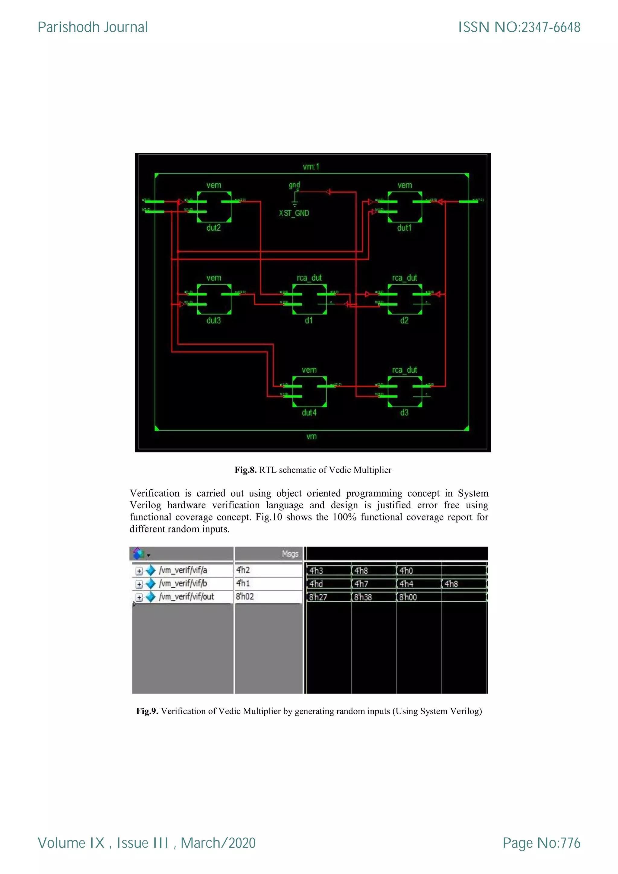
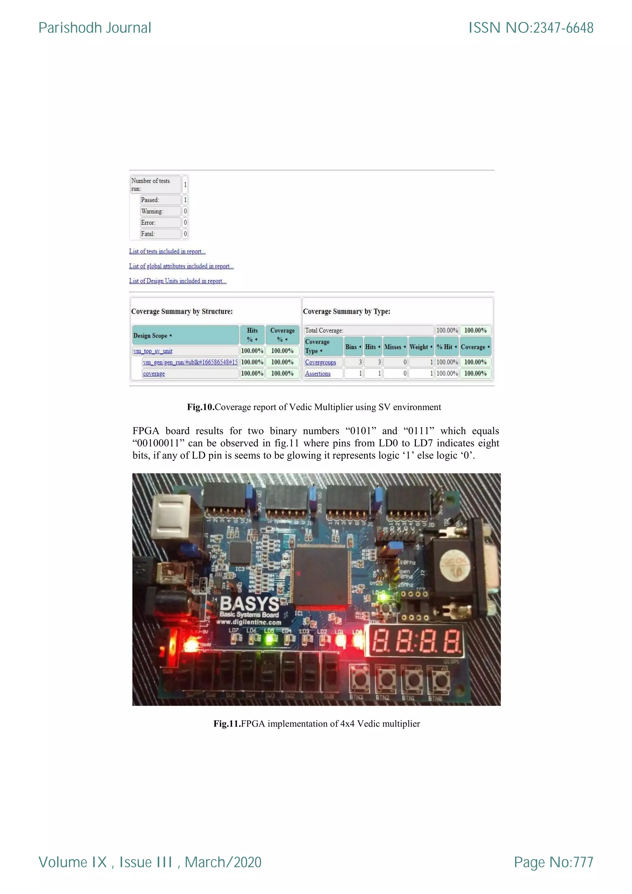

This document presents the design, verification, and FPGA implementation of a 4x4 Vedic multiplier. The multiplier is designed using Verilog HDL and verified using SystemVerilog HVL to ensure it is error-free. Simulation results show the multiplier operates correctly for different inputs. The design is also implemented on an FPGA board and shows the correct output for sample inputs. Verification covers all scenarios using functional coverage to reach 100%. The Vedic multiplier design uses the Urdhva-Triyagbhyam sutra method and is composed of smaller 2-bit multipliers along with ripple carry adders.