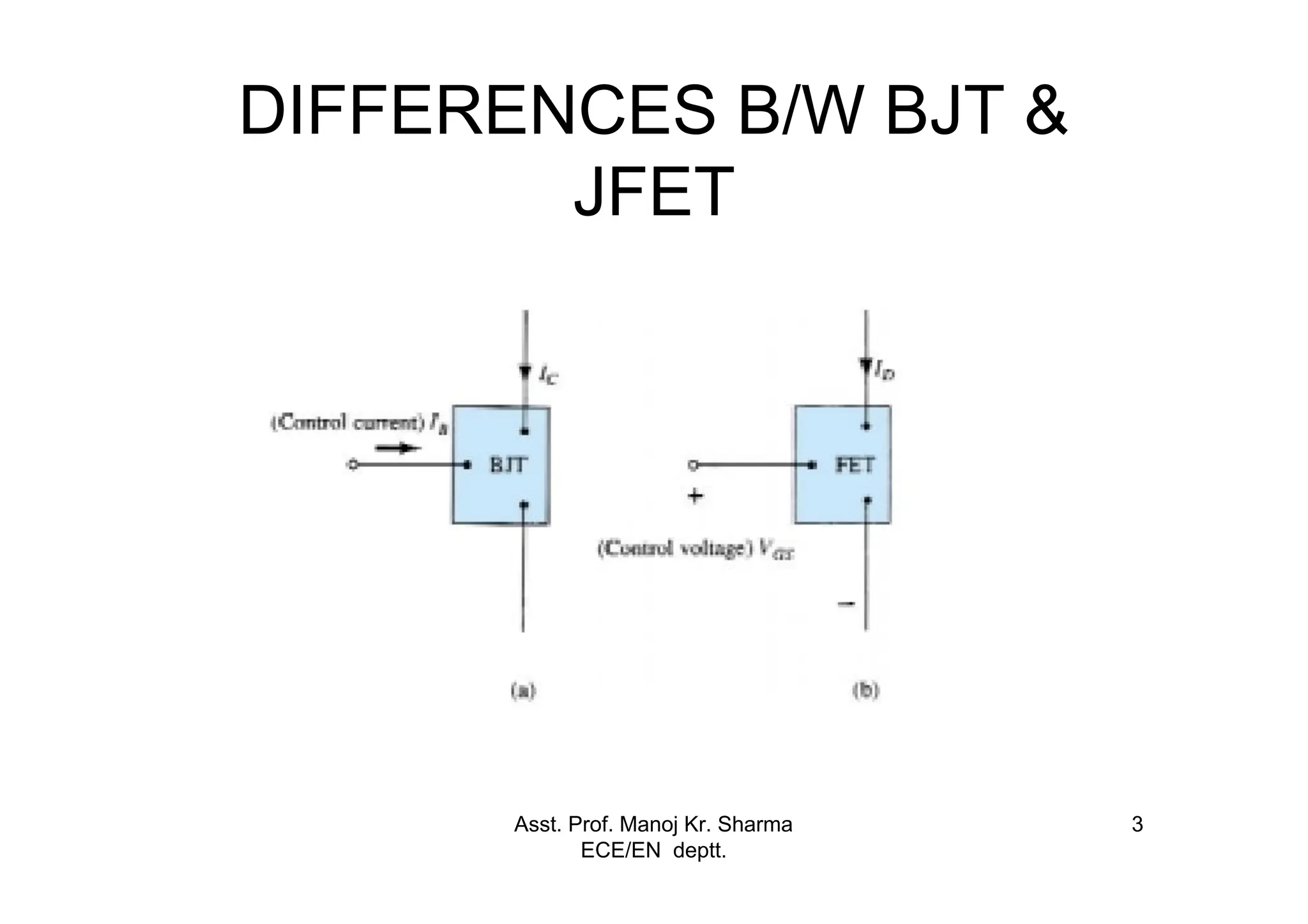
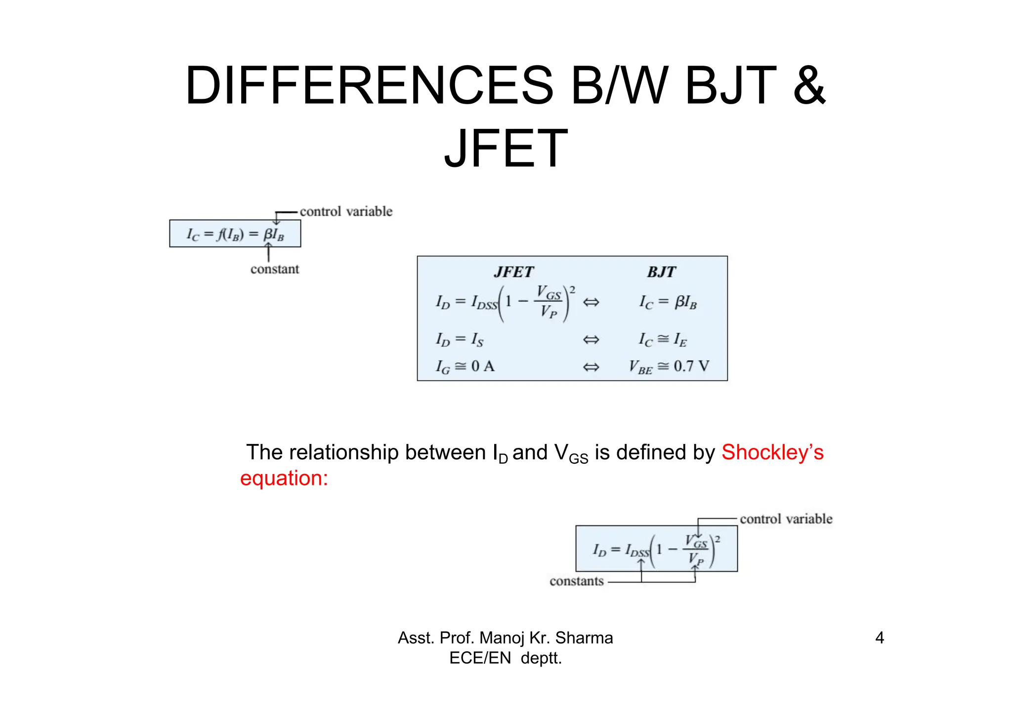
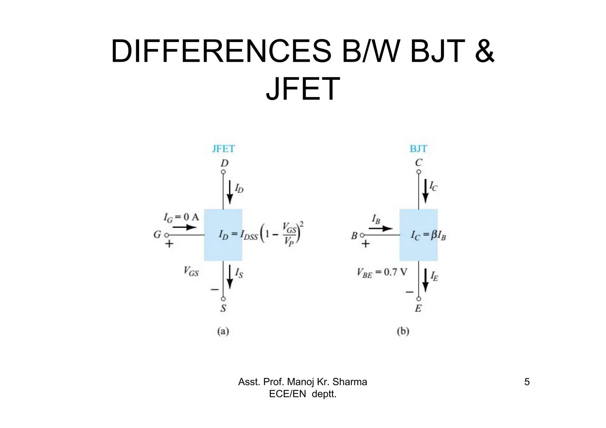
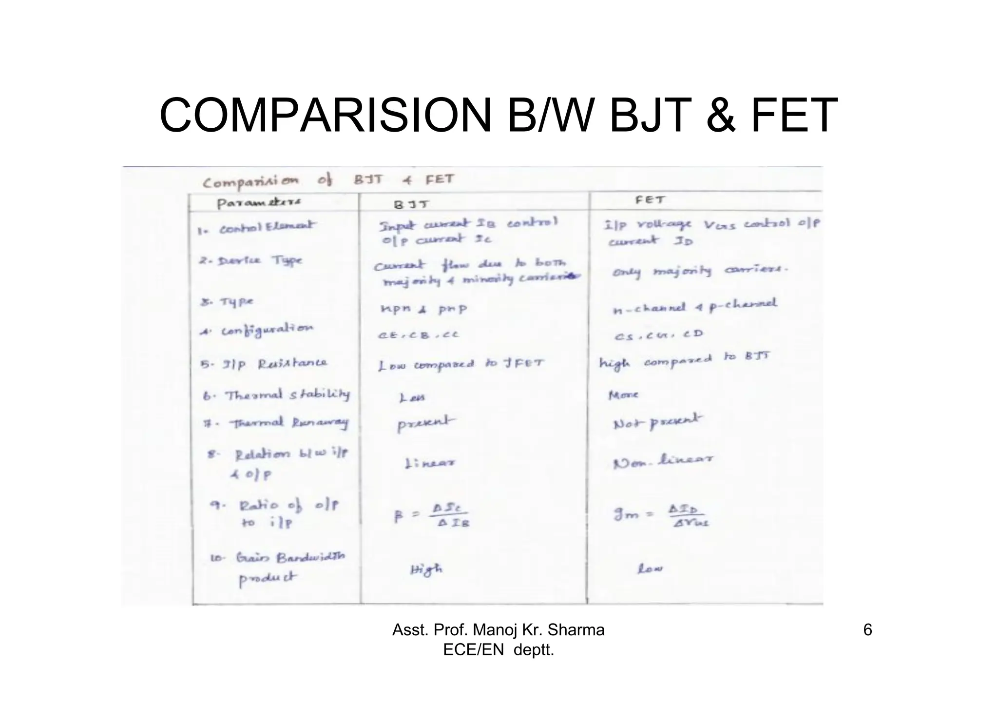
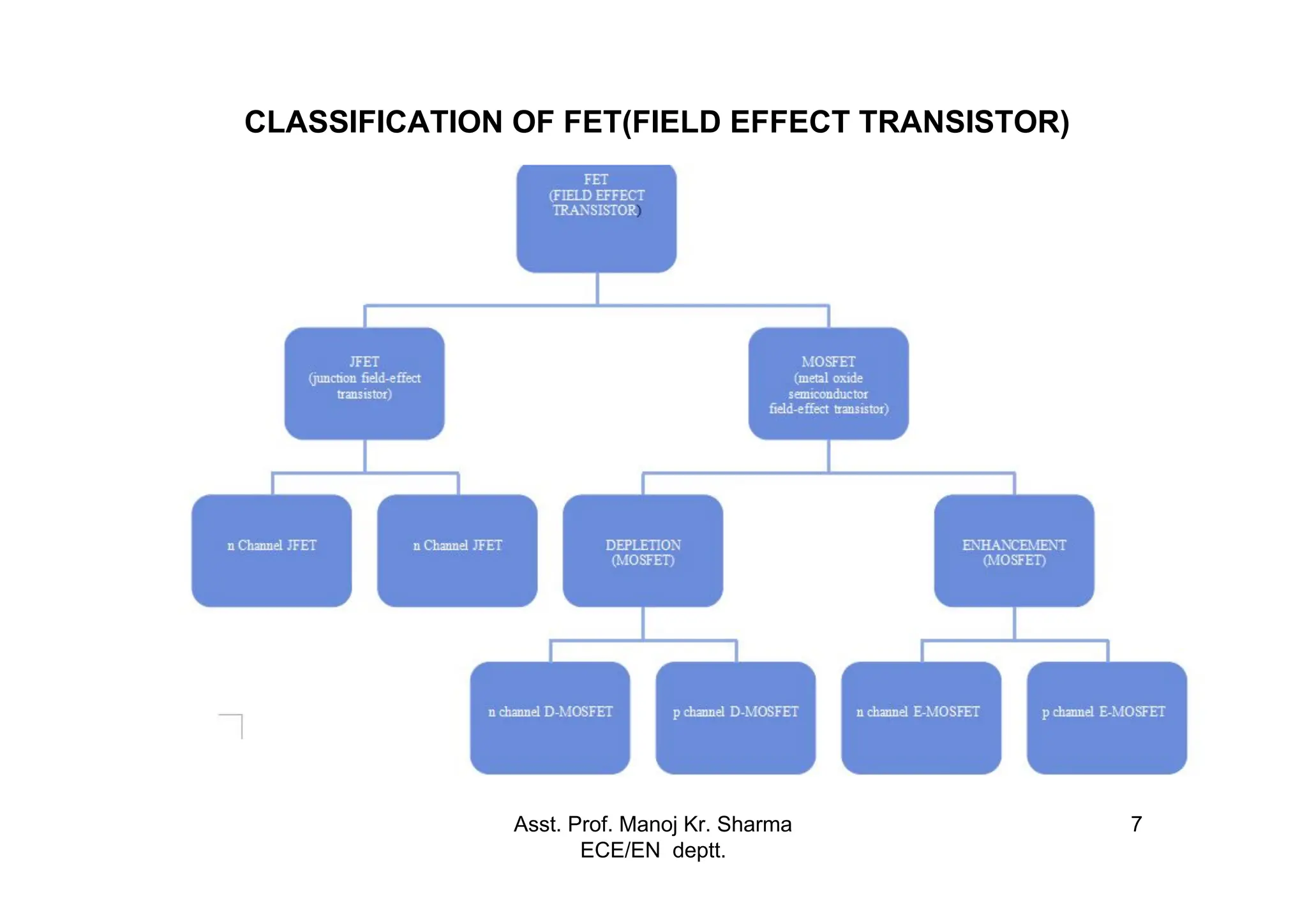
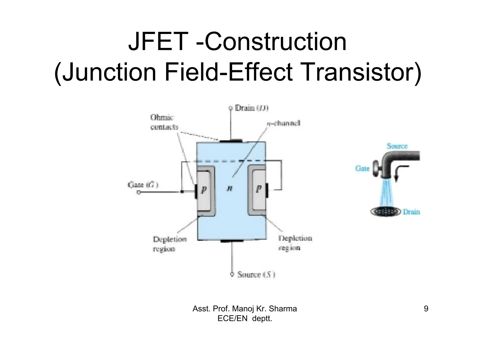
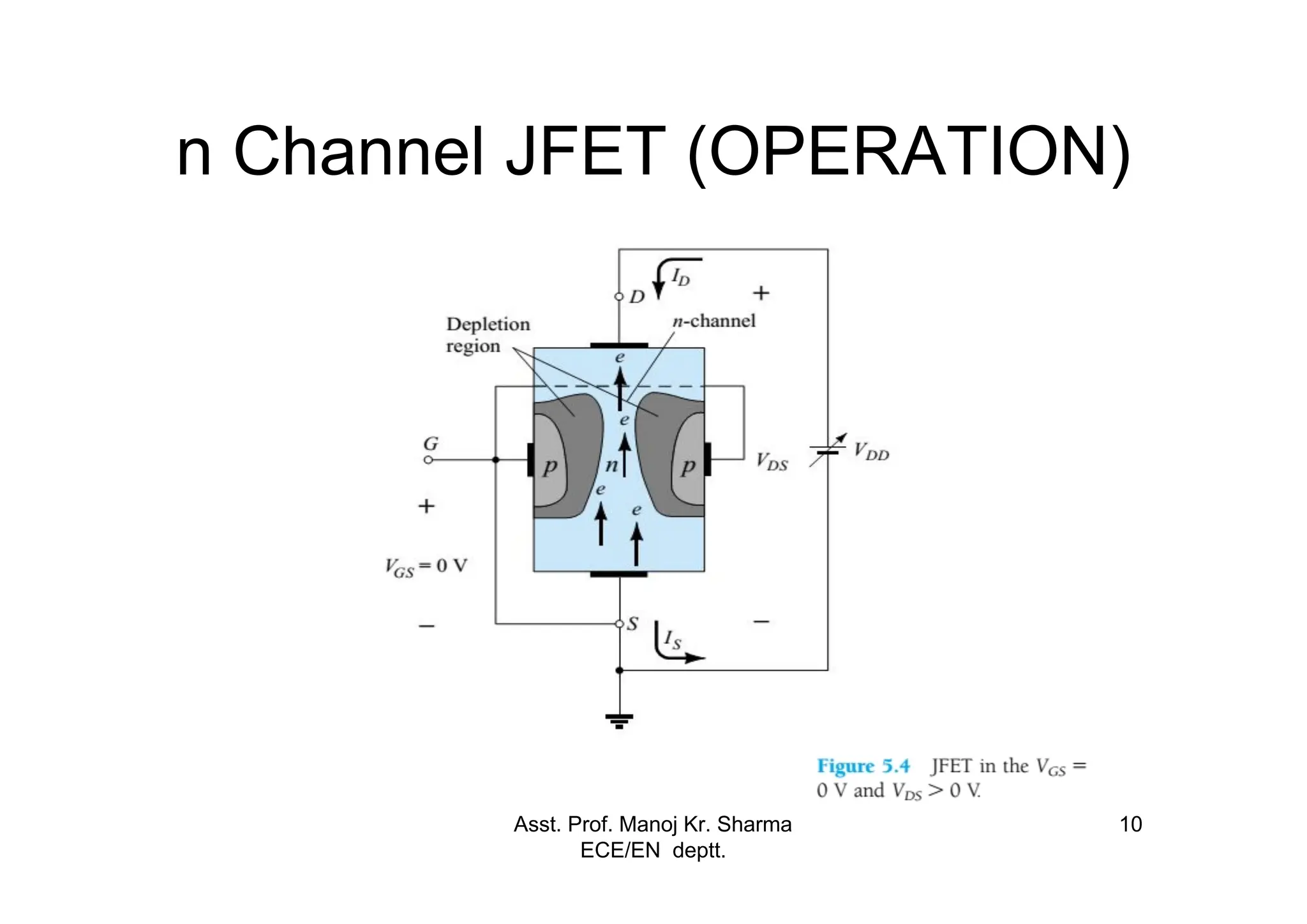
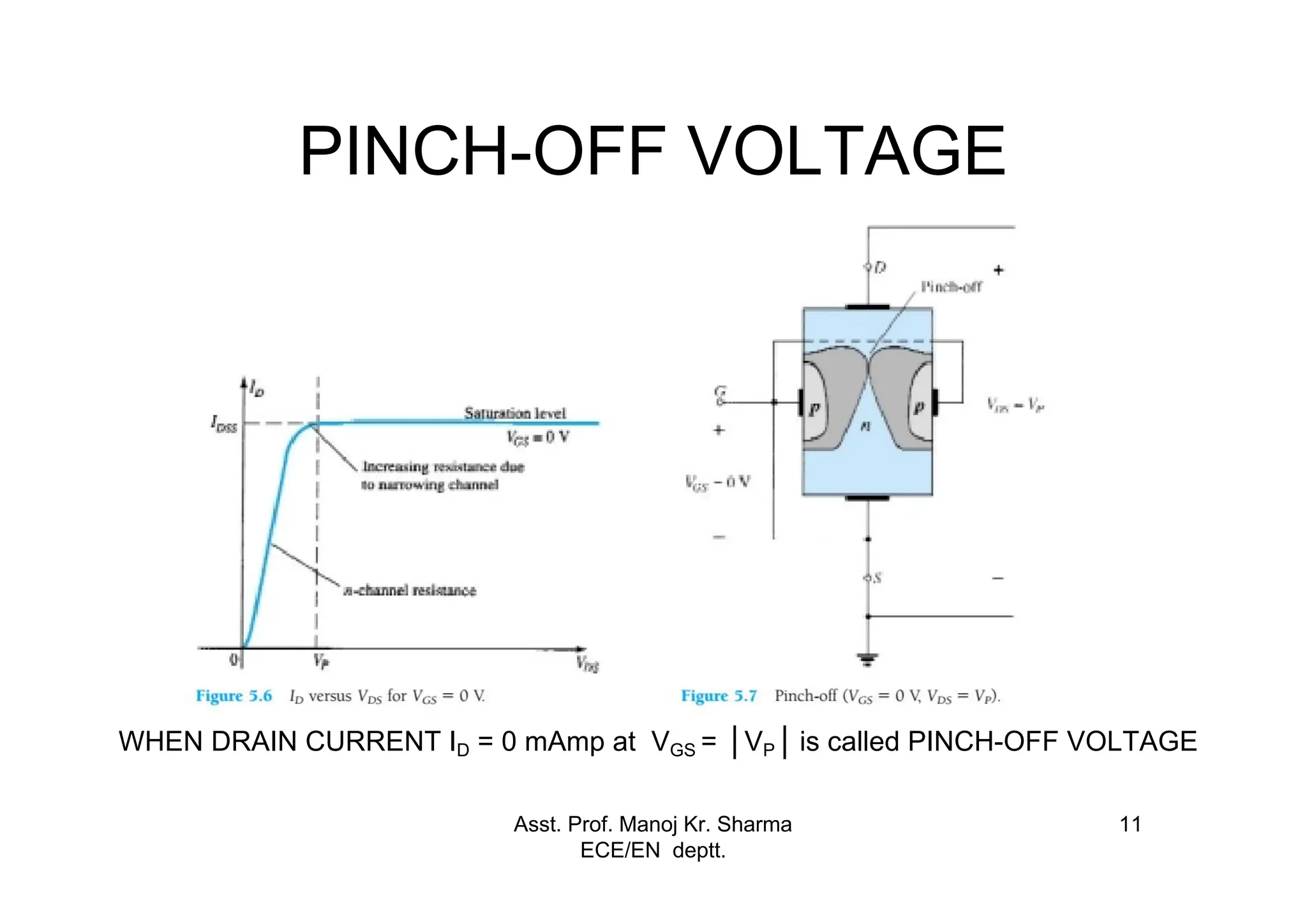
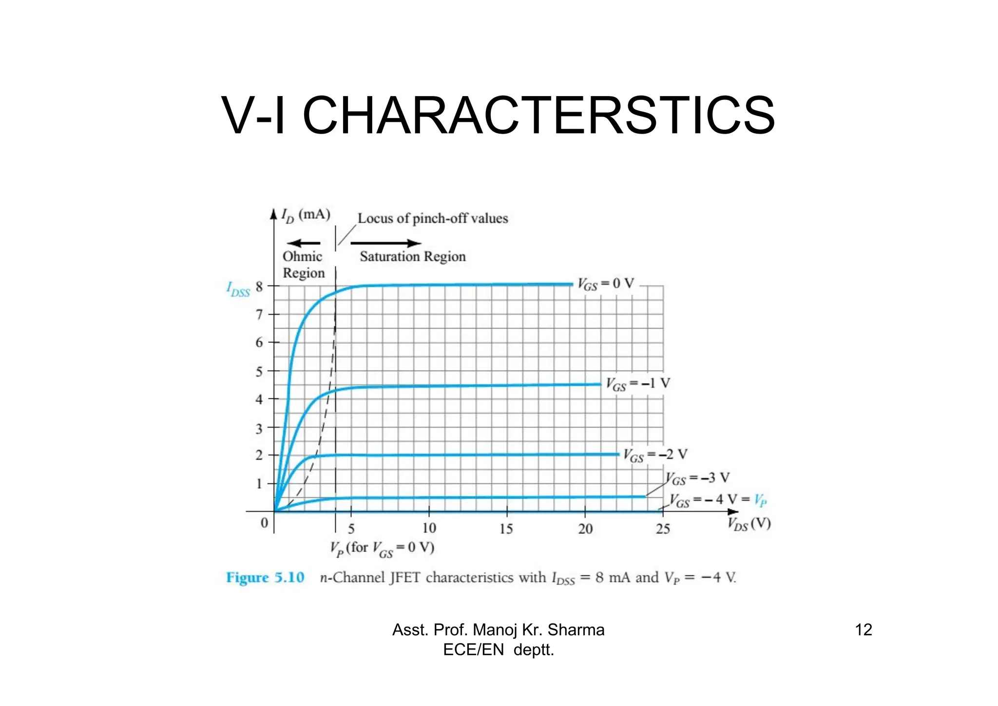
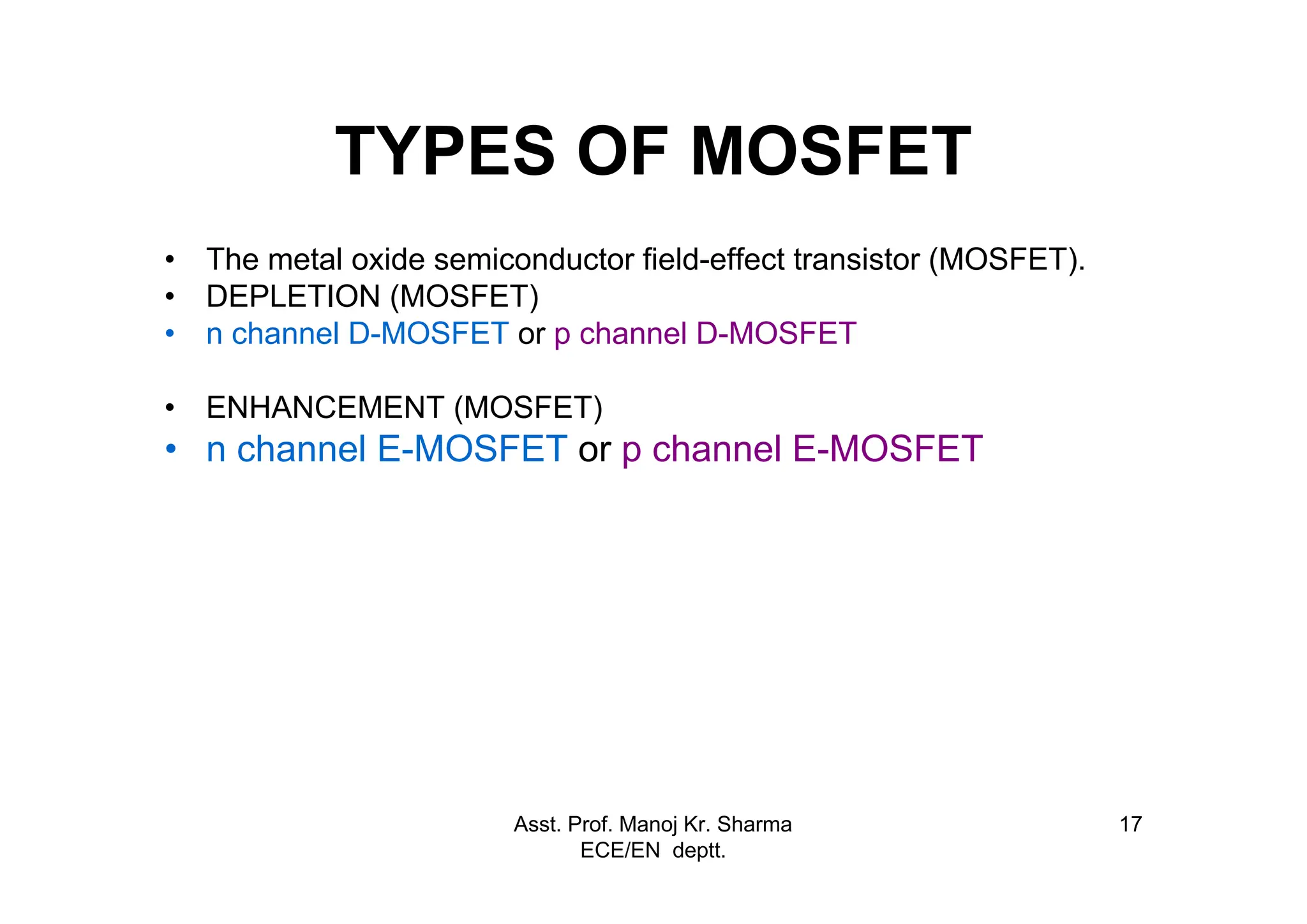
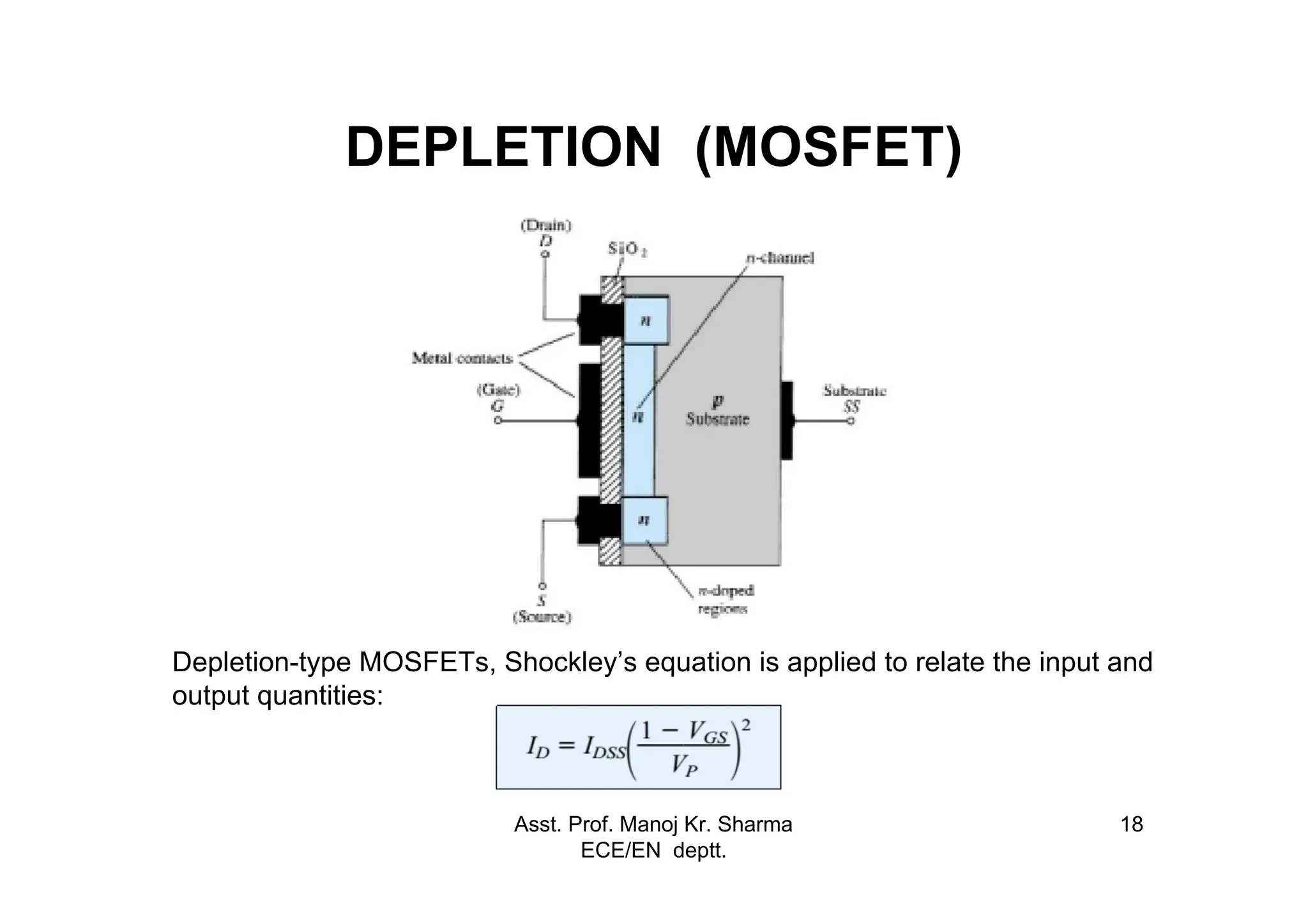
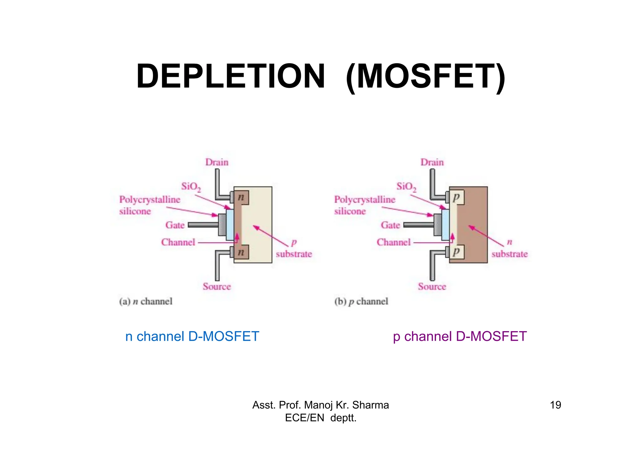
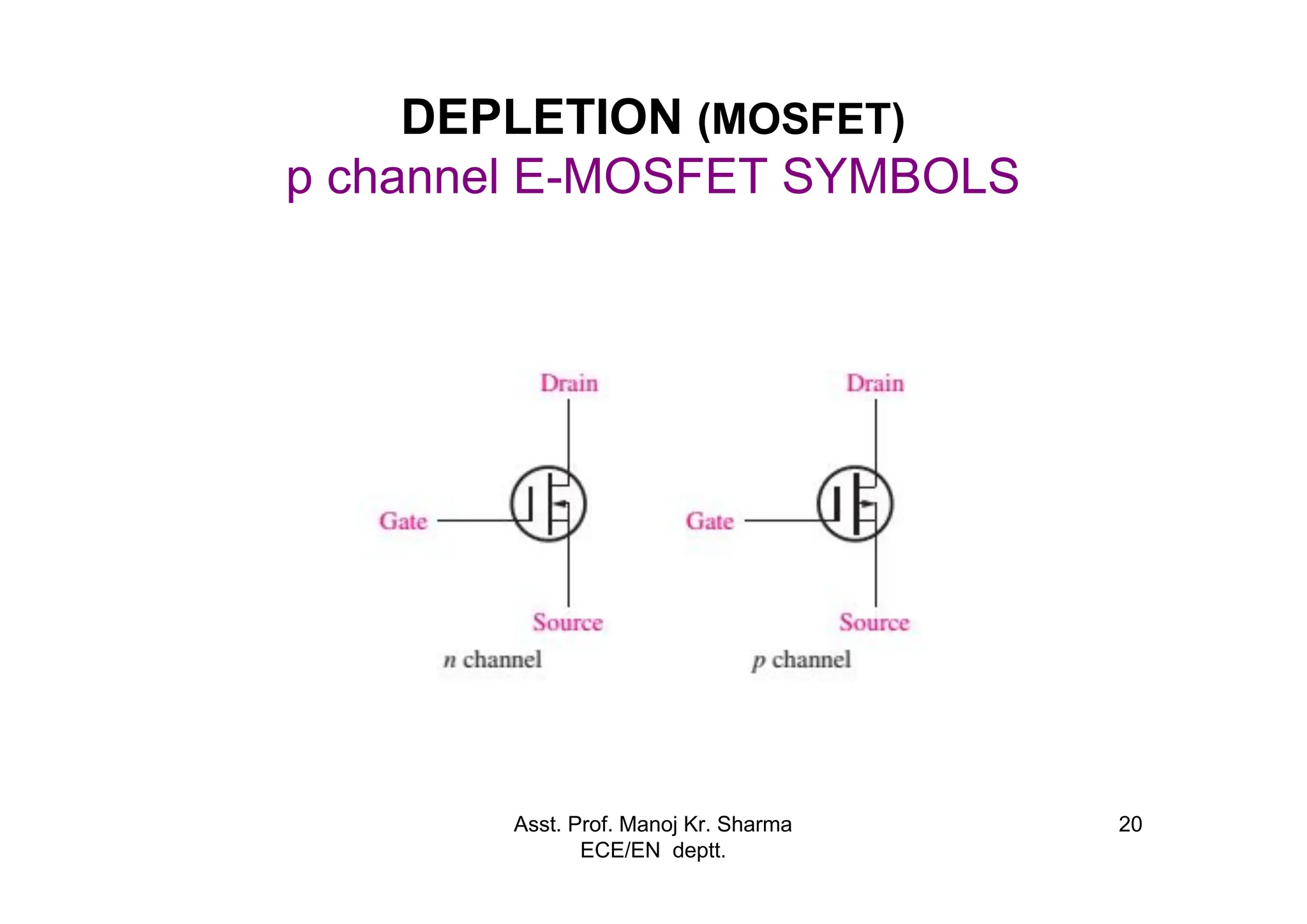
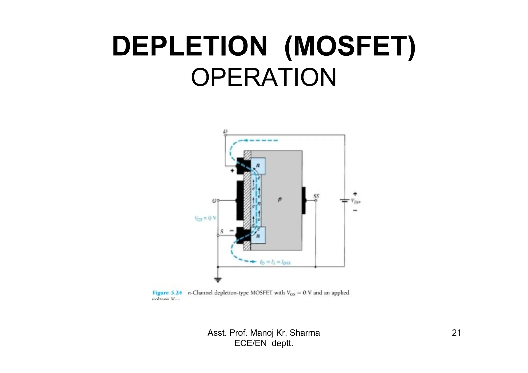
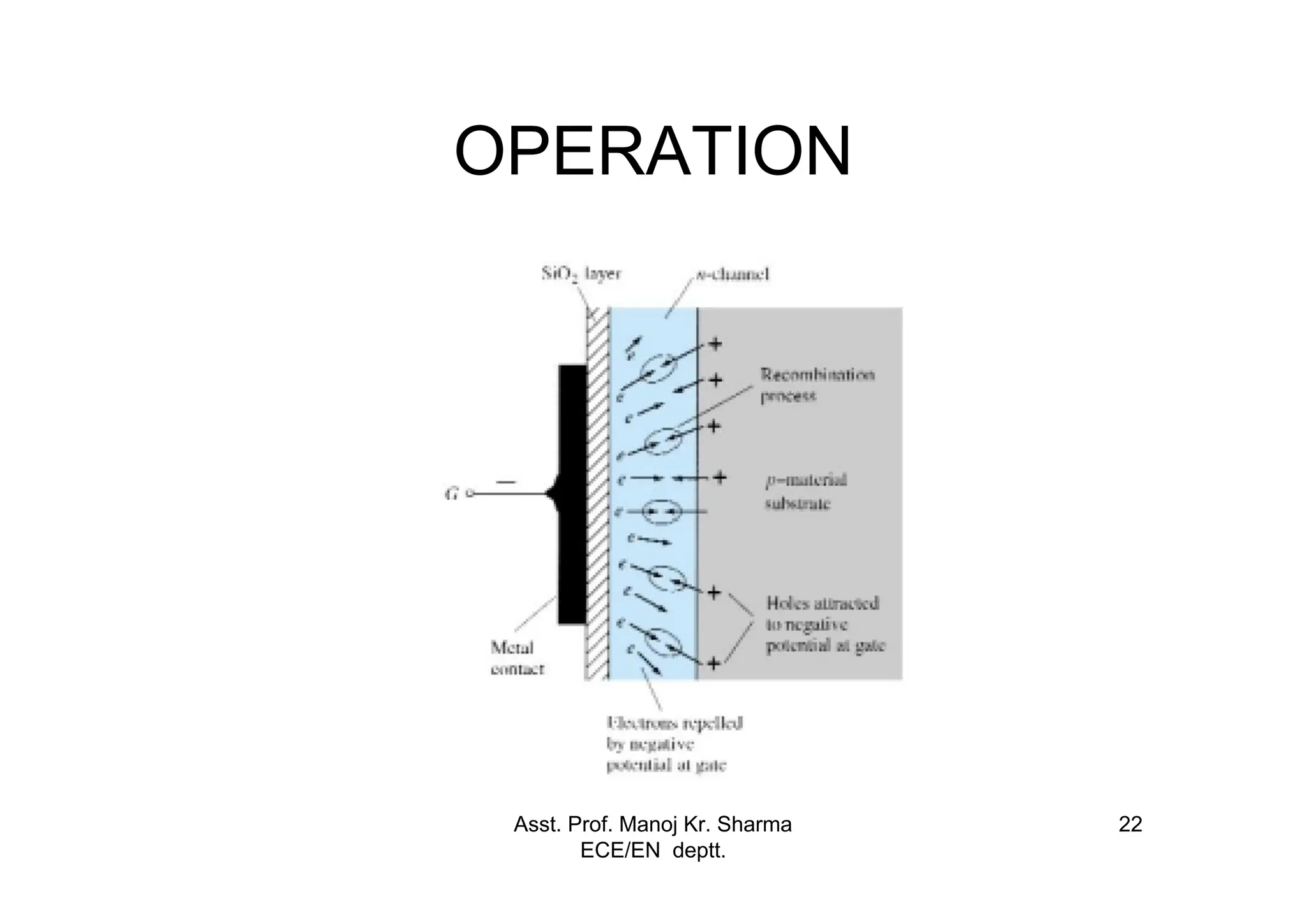
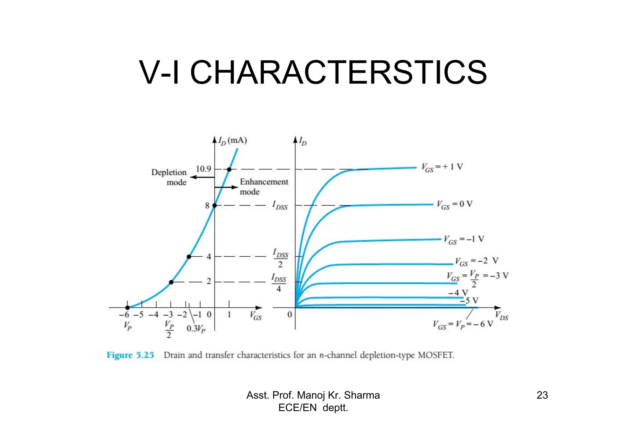
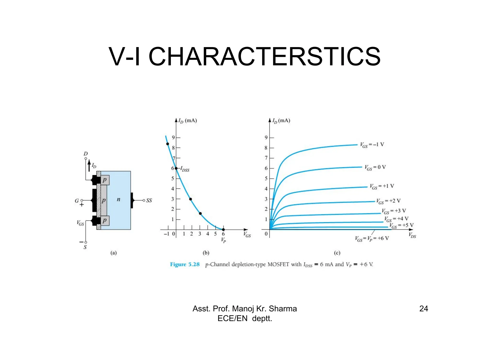
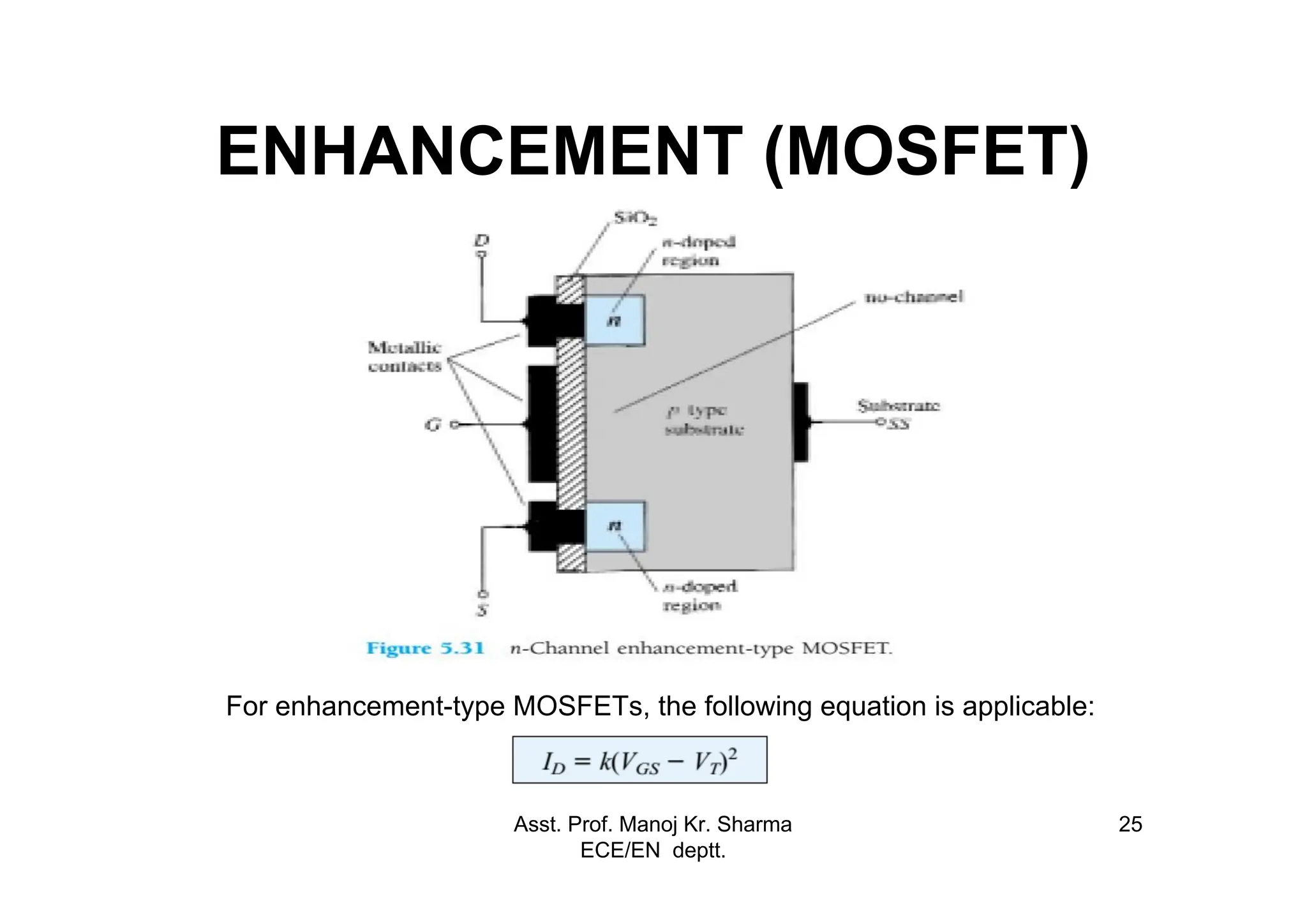
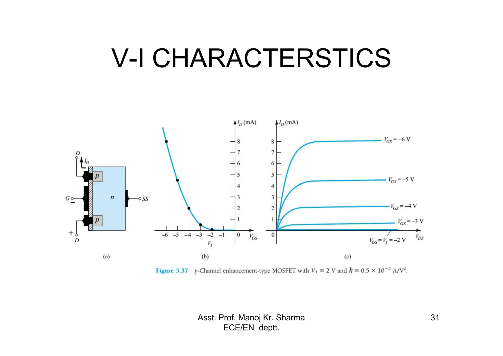
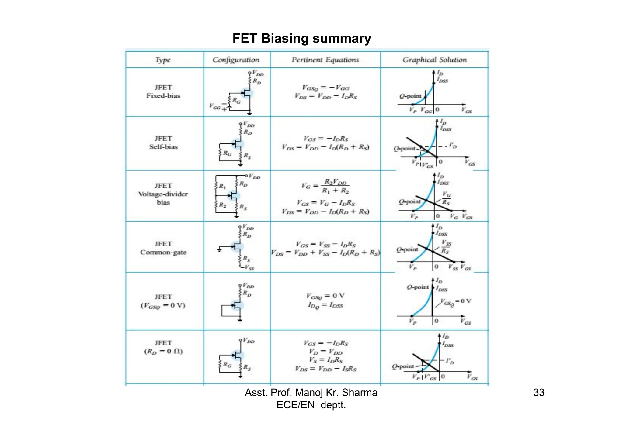
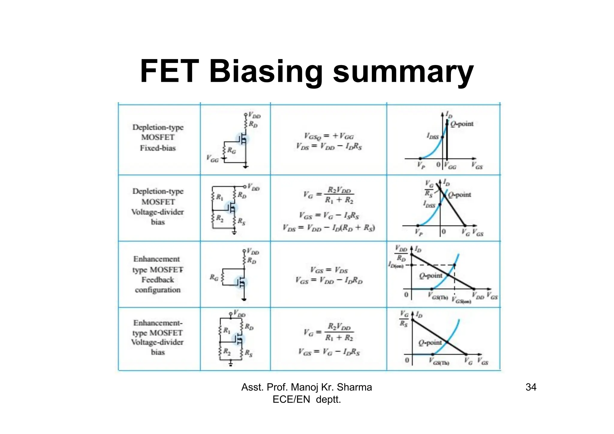
Asst. Prof. Manoj Kr. Sharma
ECE/EN deptt.
1
UNIT 2 PART B
JFET
(JUNCTION FIELD EFFECT TRANSISTOR)
The term field-effect relates to the depletion region formed in the channel
of a FET as a result of a voltage applied on one of its terminals (gate).
(OPERATION)
Asst. Prof. Manoj Kr. Sharma
ECE/EN deptt.
2
DIFFERENCES B/W BJT & JFET
• FETs are unipolar devices because, unlike BJTs that use both
electron and hole current, they operate only with one type of charge
carrier.
• Recall that a BJT is a current-controlled device; that is, the base
current controls the amount of collector current.
• A FET is different. It is a voltage-controlled device, where thevoltage
between two of the terminals (gate and source) controls the current
through the device.
• A major advantage of FETs is their very high input resistance.
• However, FETs are the preferred device in low-voltage switching
applications because they are generally faster than BJTs when
turned on and off.
Asst. Prof. Manoj Kr. Sharma
ECE/EN deptt.
3
DIFFERENCES B/W BJT &
JFET
Asst. Prof. Manoj Kr. Sharma
ECE/EN deptt.
4
DIFFERENCES B/W BJT &
JFET
The relationship between ID and VGS is defined by Shockley’s
equation:
Asst. Prof. Manoj Kr. Sharma
ECE/EN deptt.
5
DIFFERENCES B/W BJT &
JFET
Asst. Prof. Manoj Kr. Sharma
ECE/EN deptt.
6
COMPARISION B/W BJT & FET
Asst. Prof. Manoj Kr. Sharma
ECE/EN deptt.
7
CLASSIFICATION OF FET(FIELD EFFECT TRANSISTOR)
p
Asst. Prof. Manoj Kr. Sharma
ECE/EN deptt.
8
TYPES OF FET
• The JFET (junction field-effect transistor)
is a type of FET that operates with a
reverse-biased pn junction to control
current in a channel.
• Depending on their structure:
• JFETs fall into either of two categories,
n channel JFET or p channel JFET.
Asst. Prof. Manoj Kr. Sharma
ECE/EN deptt.
9
JFET -Construction
(Junction Field-Effect Transistor)
Asst. Prof. Manoj Kr. Sharma
ECE/EN deptt.
10
n Channel JFET (OPERATION)
Asst. Prof. Manoj Kr. Sharma
ECE/EN deptt.
11
PINCH-OFF VOLTAGE
WHEN DRAIN CURRENT ID = 0 mAmp at VGS = │VP│ is called PINCH-OFF VOLTAGE
Asst. Prof. Manoj Kr. Sharma
ECE/EN deptt.
12
V-I CHARACTERSTICS
Asst. Prof. Manoj Kr. Sharma
ECE/EN deptt.
13
Voltage-Controlled Resistor
In this region the JFET can actually be employed as a variable resistor
(possibly for an automatic gain control system) whose
resistance is controlled by the applied gate-to-source voltage.
Where ro is the resistance with VGS =0 V and rd the resistance at a particular level
of VGS.
For an n-channel JFET with ro equal to 10 kΩ (VGS =0 V, VP = - 6 V), above equation
will result in 40 kΩ at VGS = - 3 V.
Asst. Prof. Manoj Kr. Sharma
ECE/EN deptt.
14
V-I CHARACTERSTICS
Asst. Prof. Manoj Kr. Sharma
ECE/EN deptt.
15
P-CHANNEL JFET
Asst. Prof. Manoj Kr. Sharma
ECE/EN deptt.
16
n channel JFET & p channel JFET
SYMBOLS
Asst. Prof. Manoj Kr. Sharma
ECE/EN deptt.
17
TYPES OF MOSFET
• The metal oxide semiconductor field-effect transistor (MOSFET).
• DEPLETION (MOSFET)
• n channel D-MOSFET or p channel D-MOSFET
• ENHANCEMENT (MOSFET)
• n channel E-MOSFET or p channel E-MOSFET
Asst. Prof. Manoj Kr. Sharma
ECE/EN deptt.
18
DEPLETION (MOSFET)
Depletion-type MOSFETs, Shockley’s equation is applied to relate the input and
output quantities:
Asst. Prof. Manoj Kr. Sharma
ECE/EN deptt.
19
DEPLETION (MOSFET)
n channel D-MOSFET p channel D-MOSFET
Asst. Prof. Manoj Kr. Sharma
ECE/EN deptt.
20
DEPLETION (MOSFET)
p channel E-MOSFET SYMBOLS
Asst. Prof. Manoj Kr. Sharma
ECE/EN deptt.
21
DEPLETION (MOSFET)
OPERATION
Asst. Prof. Manoj Kr. Sharma
ECE/EN deptt.
22
OPERATION
Asst. Prof. Manoj Kr. Sharma
ECE/EN deptt.
23
V-I CHARACTERSTICS
Asst. Prof. Manoj Kr. Sharma
ECE/EN deptt.
24
V-I CHARACTERSTICS
Asst. Prof. Manoj Kr. Sharma
ECE/EN deptt.
25
ENHANCEMENT (MOSFET)
For enhancement-type MOSFETs, the following equation is applicable:
Asst. Prof. Manoj Kr. Sharma
ECE/EN deptt.
26
ENHANCEMENT (MOSFET)
n channel E-MOSFET
Asst. Prof. Manoj Kr. Sharma
ECE/EN deptt.
27
ENHANCEMENT (MOSFET)
SYMBOLS
Asst. Prof. Manoj Kr. Sharma
ECE/EN deptt.
28
n channel E-MOSFET(OPERATION)
Asst. Prof. Manoj Kr. Sharma
ECE/EN deptt.
29
n channel E-MOSFET OPERATION
Asst. Prof. Manoj Kr. Sharma
ECE/EN deptt.
30
V-I CHARACTERSTICS
Asst. Prof. Manoj Kr. Sharma
ECE/EN deptt.
31
V-I CHARACTERSTICS
Asst. Prof. Manoj Kr. Sharma
ECE/EN deptt.
32
FET Biasing
• FIXED-BIAS CONFIGURATION
• SELF-BIAS CONFIGURATION
• VOLTAGE-DIVIDER BIASING
Asst. Prof. Manoj Kr. Sharma
ECE/EN deptt.
33
FET Biasing summary
Asst. Prof. Manoj Kr. Sharma
ECE/EN deptt.
34
FET Biasing summary

Basic construction and operation FET and MOSFET PPT UNIT 2.pdf

  • 1.
    Asst. Prof. ManojKr. Sharma ECE/EN deptt. 1 UNIT 2 PART B JFET (JUNCTION FIELD EFFECT TRANSISTOR) The term field-effect relates to the depletion region formed in the channel of a FET as a result of a voltage applied on one of its terminals (gate). (OPERATION)
  • 2.
    Asst. Prof. ManojKr. Sharma ECE/EN deptt. 2 DIFFERENCES B/W BJT & JFET • FETs are unipolar devices because, unlike BJTs that use both electron and hole current, they operate only with one type of charge carrier. • Recall that a BJT is a current-controlled device; that is, the base current controls the amount of collector current. • A FET is different. It is a voltage-controlled device, where thevoltage between two of the terminals (gate and source) controls the current through the device. • A major advantage of FETs is their very high input resistance. • However, FETs are the preferred device in low-voltage switching applications because they are generally faster than BJTs when turned on and off.
  • 3.
    Asst. Prof. ManojKr. Sharma ECE/EN deptt. 3 DIFFERENCES B/W BJT & JFET
  • 4.
    Asst. Prof. ManojKr. Sharma ECE/EN deptt. 4 DIFFERENCES B/W BJT & JFET The relationship between ID and VGS is defined by Shockley’s equation:
  • 5.
    Asst. Prof. ManojKr. Sharma ECE/EN deptt. 5 DIFFERENCES B/W BJT & JFET
  • 6.
    Asst. Prof. ManojKr. Sharma ECE/EN deptt. 6 COMPARISION B/W BJT & FET
  • 7.
    Asst. Prof. ManojKr. Sharma ECE/EN deptt. 7 CLASSIFICATION OF FET(FIELD EFFECT TRANSISTOR) p
  • 8.
    Asst. Prof. ManojKr. Sharma ECE/EN deptt. 8 TYPES OF FET • The JFET (junction field-effect transistor) is a type of FET that operates with a reverse-biased pn junction to control current in a channel. • Depending on their structure: • JFETs fall into either of two categories, n channel JFET or p channel JFET.
  • 9.
    Asst. Prof. ManojKr. Sharma ECE/EN deptt. 9 JFET -Construction (Junction Field-Effect Transistor)
  • 10.
    Asst. Prof. ManojKr. Sharma ECE/EN deptt. 10 n Channel JFET (OPERATION)
  • 11.
    Asst. Prof. ManojKr. Sharma ECE/EN deptt. 11 PINCH-OFF VOLTAGE WHEN DRAIN CURRENT ID = 0 mAmp at VGS = │VP│ is called PINCH-OFF VOLTAGE
  • 12.
    Asst. Prof. ManojKr. Sharma ECE/EN deptt. 12 V-I CHARACTERSTICS
  • 13.
    Asst. Prof. ManojKr. Sharma ECE/EN deptt. 13 Voltage-Controlled Resistor In this region the JFET can actually be employed as a variable resistor (possibly for an automatic gain control system) whose resistance is controlled by the applied gate-to-source voltage. Where ro is the resistance with VGS =0 V and rd the resistance at a particular level of VGS. For an n-channel JFET with ro equal to 10 kΩ (VGS =0 V, VP = - 6 V), above equation will result in 40 kΩ at VGS = - 3 V.
  • 14.
    Asst. Prof. ManojKr. Sharma ECE/EN deptt. 14 V-I CHARACTERSTICS
  • 15.
    Asst. Prof. ManojKr. Sharma ECE/EN deptt. 15 P-CHANNEL JFET
  • 16.
    Asst. Prof. ManojKr. Sharma ECE/EN deptt. 16 n channel JFET & p channel JFET SYMBOLS
  • 17.
    Asst. Prof. ManojKr. Sharma ECE/EN deptt. 17 TYPES OF MOSFET • The metal oxide semiconductor field-effect transistor (MOSFET). • DEPLETION (MOSFET) • n channel D-MOSFET or p channel D-MOSFET • ENHANCEMENT (MOSFET) • n channel E-MOSFET or p channel E-MOSFET
  • 18.
    Asst. Prof. ManojKr. Sharma ECE/EN deptt. 18 DEPLETION (MOSFET) Depletion-type MOSFETs, Shockley’s equation is applied to relate the input and output quantities:
  • 19.
    Asst. Prof. ManojKr. Sharma ECE/EN deptt. 19 DEPLETION (MOSFET) n channel D-MOSFET p channel D-MOSFET
  • 20.
    Asst. Prof. ManojKr. Sharma ECE/EN deptt. 20 DEPLETION (MOSFET) p channel E-MOSFET SYMBOLS
  • 21.
    Asst. Prof. ManojKr. Sharma ECE/EN deptt. 21 DEPLETION (MOSFET) OPERATION
  • 22.
    Asst. Prof. ManojKr. Sharma ECE/EN deptt. 22 OPERATION
  • 23.
    Asst. Prof. ManojKr. Sharma ECE/EN deptt. 23 V-I CHARACTERSTICS
  • 24.
    Asst. Prof. ManojKr. Sharma ECE/EN deptt. 24 V-I CHARACTERSTICS
  • 25.
    Asst. Prof. ManojKr. Sharma ECE/EN deptt. 25 ENHANCEMENT (MOSFET) For enhancement-type MOSFETs, the following equation is applicable:
  • 26.
    Asst. Prof. ManojKr. Sharma ECE/EN deptt. 26 ENHANCEMENT (MOSFET) n channel E-MOSFET
  • 27.
    Asst. Prof. ManojKr. Sharma ECE/EN deptt. 27 ENHANCEMENT (MOSFET) SYMBOLS
  • 28.
    Asst. Prof. ManojKr. Sharma ECE/EN deptt. 28 n channel E-MOSFET(OPERATION)
  • 29.
    Asst. Prof. ManojKr. Sharma ECE/EN deptt. 29 n channel E-MOSFET OPERATION
  • 30.
    Asst. Prof. ManojKr. Sharma ECE/EN deptt. 30 V-I CHARACTERSTICS
  • 31.
    Asst. Prof. ManojKr. Sharma ECE/EN deptt. 31 V-I CHARACTERSTICS
  • 32.
    Asst. Prof. ManojKr. Sharma ECE/EN deptt. 32 FET Biasing • FIXED-BIAS CONFIGURATION • SELF-BIAS CONFIGURATION • VOLTAGE-DIVIDER BIASING
  • 33.
    Asst. Prof. ManojKr. Sharma ECE/EN deptt. 33 FET Biasing summary
  • 34.
    Asst. Prof. ManojKr. Sharma ECE/EN deptt. 34 FET Biasing summary