The document summarizes research on a tristable non-volatile memory device with a simple three-layer stacking structure consisting of a molybdenum disulfide (MoS2) flakes-graphene quantum dots (GQDs) heterostructure charge trapping layer embedded in polyvinylidene fluoride (PVDF) polymer. Transmission electron microscopy showed the MoS2-GQD heterostructure had misaligned orientations. Electrical measurements found the device exhibited tristable switching behavior with a high ON/OFF current ratio of 107, attributed to the high charge storage capability of the MoS2-GQD heterostructure. This demonstrated the potential for high density data storage using a single charge trapping layer.
![2
Scientific Reports | (2019) 9:6761 | https://doi.org/10.1038/s41598-019-43279-3
www.nature.com/scientificreports
www.nature.com/scientificreports/
less induced heat and attained device size miniaturization as compared to the reported work by Ooi et al.4
, that
comprises of two charge layers in their fabricated device. MoS2 and GQD, the 2D-NPs with dimensions down to
atomic level, have attracted high attention due to their fascinating properties in wide range of developments on
the next generation of miniaturized electronic applications such as optoelectronics, optically transparent, and
mechanically flexible devices10–14
.
MoS2 NPs have been identified as a promising material for switching device application due to its high
work function, quantum confinement effect, a direct band gap of 1.8 eV in monolayer, and a high mobility of
200 cm2
V−1
s−1
with a high current ON/OFF ratio at approximately 108
when used as channel materials in field
effect transistors geometry15–17
. The monolayer MoS2 is very sensitive to the presence of charges but it demon-
strates the drawbacks of relatively small hysteresis window with degraded mobility and insufficient charge trap
capability that might be correlated to charge trap stacking issue when it is constructed in a MIM geometry10,17
.
Therefore, the nanometer-sized GQD will be integrated with MoS2 flake to create a MoS2-GQD heterostructure
charge trap medium to enhance data storage capacity and retention time. This integration is possible because of
semi-metallic properties of GQD that could form the ideal contact with MoS2, and thus capable of supporting
large current density, exceeding 109
A/m2 18–20
. Moreover, the lack of dangling bonds at the interface between
graphene and those 2D semiconductors would suppress the formation of interface states and charge traps18
.
As aforementioned, the blend of GQDs and MoS2 NPs will be dispersed in PVDF polymer to form a
GQD-MoS2-PVDF nanocomposite (GMP-NC). PVDF polymer is used as dielectric barrier in this work owing to
its flexibility, low weight, and low-cost solution processability. In addition, PVDF is also a non-reactive nature and
possesses better heat resistance21,22
. A switching device will be fabricated on indium-tin-oxide (ITO) coated glass
substrate using simple solution process route in the structure of GMP-NC layer in between the PVDF dielectric
layers. Solution-processing deposition is exploited as one of the promising methods to realize a low-cost and sim-
ple method for the construction of optically transparent and mechanically flexible electronic devices. Moreover,
this method could avoid expensive and tedious fabrication process such as time-consuming operational steps,
high-temperature mean, and costly vacuum environment9,23
.
Results
Lattice-resolved characterization of GQDs-MoS2 heterostructure. The atomic structure of the
GQDs-MoS2 heterostructure that is incorporated into the fabricated device structure was characterized by
high-resolution transmission electron microscopy (HR-TEM). Figure 1(a) displays a low-magnification bright-
field TEM image of a MoS2 flake decorated with GQDs, illustrating a stacked few-layer MoS2 from the visibility
of color contrast along the edges due to interlayer coupling behavior of the exfoliated natural crystals. Few folded
and disorder regions can be observed at the edges, indicating possible lattice defects, dislocation, or local stresses
in the MoS2 layer. A higher magnification image in Fig. 1(b) shows that the GQDs with different sizes up to
~10 nm is closely packed together on the MoS2 flake. In Fig. 1(c), high-resolution TEM shows multi-layer MoS2
with interlayer spacing of ~0.62 nm, which corresponds to the MoS2 (002) lattice plane. The GQDs are expected
to be misaligned on the MoS2 flake, as evidenced by the Fourier filtered HR-TEM image in Fig. 1(d). Notably,
the result shows clear Moiré patterns (indicated by the green square area) in between the MoS2 edges due to mis-
orientation between a single GQD and MoS2 layers, which is further confirmed by fast Fourier transform (FFT)
pattern of the HRTEM image, as shown by the insert in Fig. 1(d). At this region, two sets of hexagonally arranged
diffraction spots that originated from GQD (white) and MoS2 (yellow) with a rotation angle of ~29.3° can be
observed, indicate the single-crystalline nature of GQD and MoS2. Considering that MoS2 has larger lattice con-
stant (a = 0.312 nm) than that of GQD (a = 0.246 nm), the diffraction spots from the first order of MoS2 should be
located closer to the center of the electron beam. In addition, most of the GQDs are expected to be oriented ran-
domly on the MoS2 flake by our dispersion method, which is further confirmed by typical Debye-Scherrer type
ring pattern of graphene crystals from the FFT pattern (Refer to Supplementary Information, Fig. S1). HRTEM
and selected area electron diffraction (SAED) characterization on individual GQD and MoS2 were also employed
to further confirm the pristine nature of these 2D NPs. Both HRTEM images of GQD and few-layer MoS2 and
their corresponding FFT patterns in Fig. 1(e,f) show the characteristic of single-crystalline lattice structure. Based
on the corresponding SAED images with [001] zone axis, hexagonal lattice structures are clearly visible for both
GQD and few-layer MoS2 as shown in Fig. 1(g,h), which are consistent with the literatures24,25
. Here, the lattice
spacing for the GQD can be evaluated to be ~0.25 nm and ~0.14 nm corresponding to the (100) and (110) planes,
respectively. Meanwhile, the few-layer MoS2 reveals lattice spacing of ~0.27 nm and ~0.16 nm for the (100) and
(110) planes, respectively. Furthermore, individual C, Mo, and S atom can also be resolved in the hexagonal pack-
ing arrangement from the Fourier filtered HRTEM images of GQD and few-layer MoS2, as shown in Fig. 1(i,j).
These images were processed from the raw HRTEM images (indicated by red square area) in Fig. 1(e,f) by using
Fourier mask filtering method [18, 19]. As shown in Fig. 1(g,h), the line profiles of contrasting intensities along
the zigzag direction reveal a hexagonal lattice spacing of ~2.5 Å and ~3.2 Å for the GQD and few-layer MoS2,
respectively. On the other hand, analysis of the contrasting intensities along the armchair direction shows the C
atoms and Mo-S atoms is separated by ~1.4 Å and ~2.4 Å, respectively.
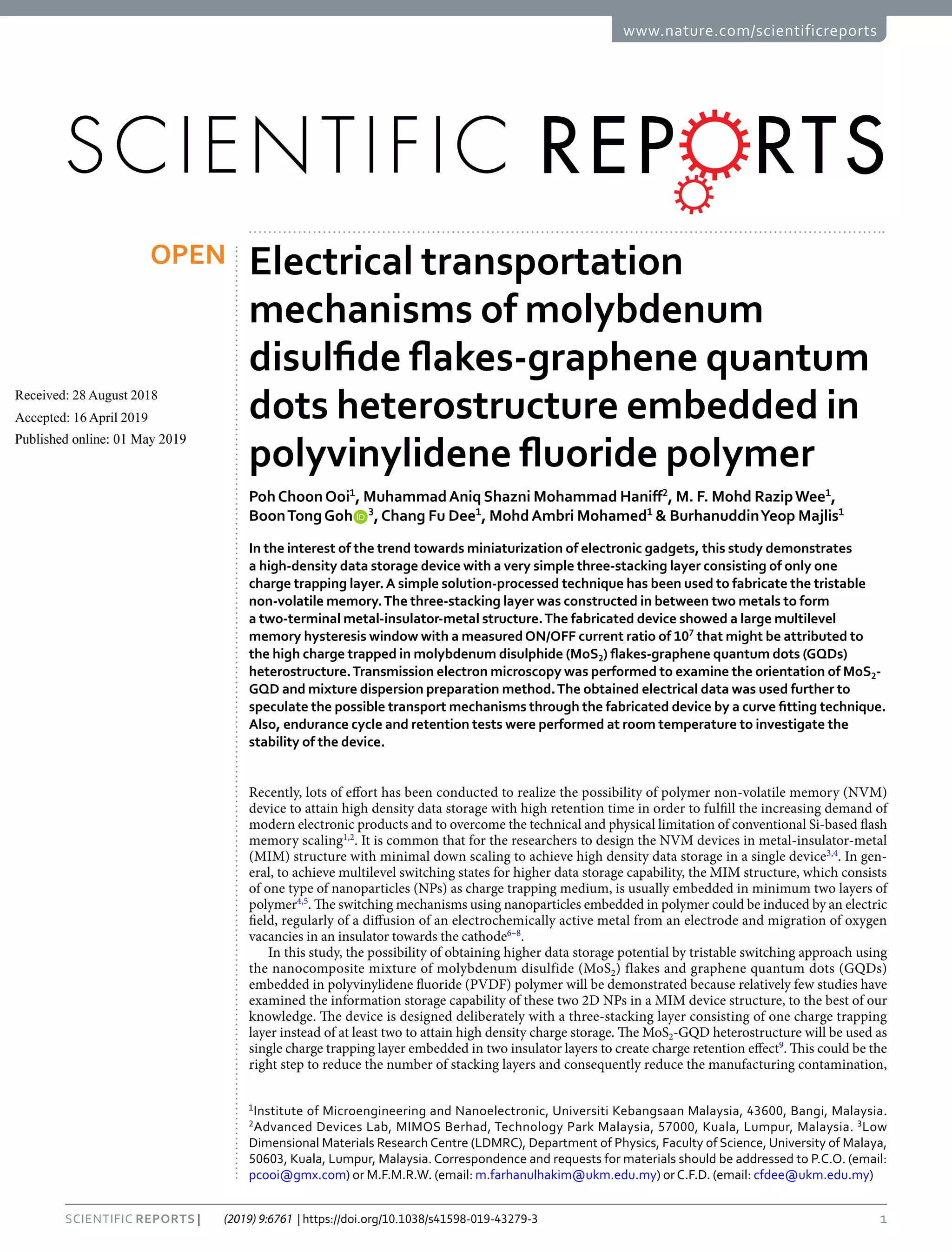
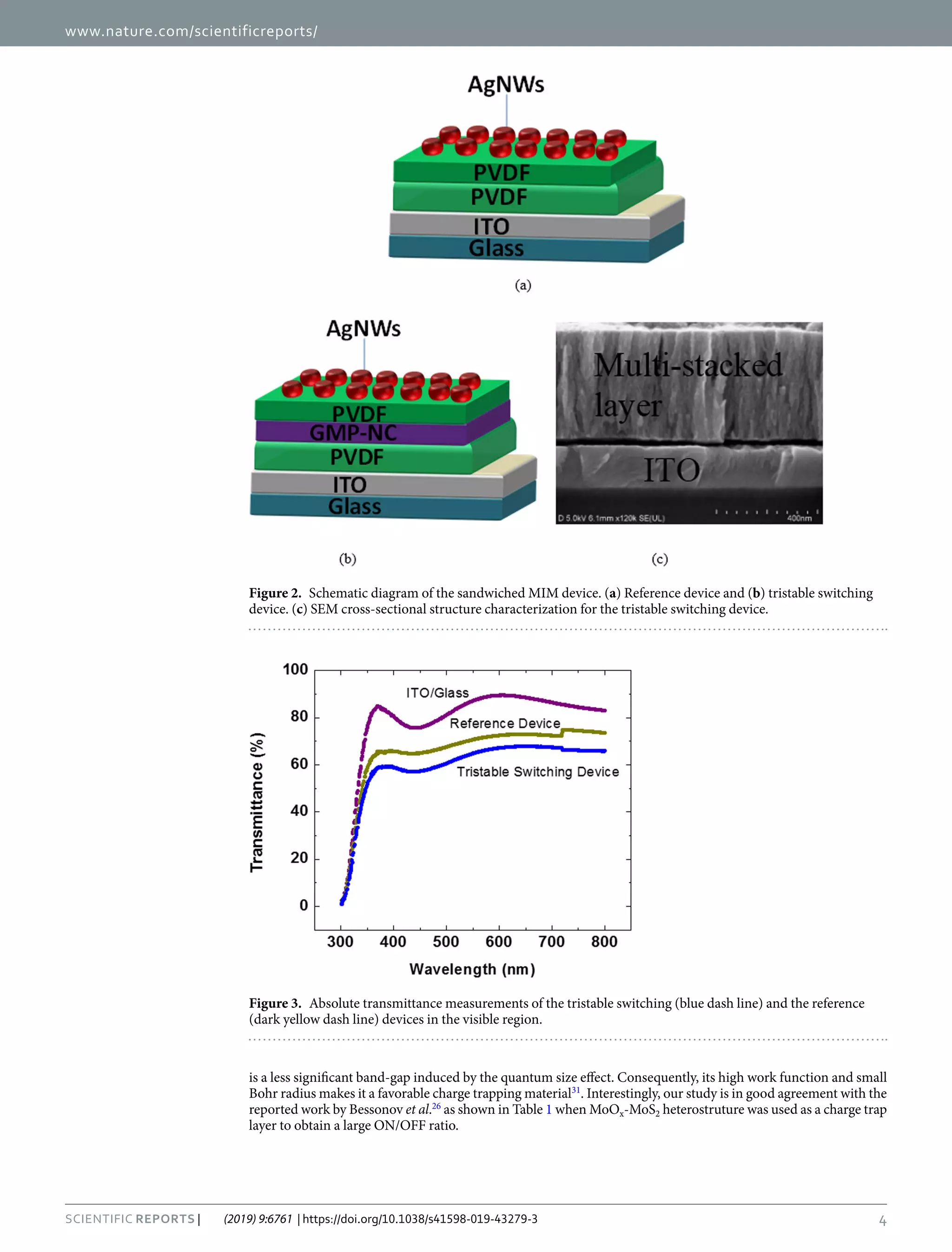
Transmittance and electrical measurements of the fabricated devices. Figure 2(a,b) depict the
sandwiched structure of the reference and tristable switching devices. Figure 2(c) presents a SEM cross-section
image of the tristable switching device with multi-stacked layer on ITO layer. Figure 3 shows the transparency
measurements for the fabricated reference and tristable switching-device when compared to the ITO/glass sub-
strate in the visible spectral range from 400 to 800 nm. The plot of purple dash line indicating the percentage of
absolute transmittance for ITO/glass substrate varies from 80.4 to 89.5%, whereas the blue and dark yellow dash
lines show the absolute transmittances change from 58.8 to 67.8% and 65.7 to 74.9% for the tristable switch-
ing device and reference device, respectively. The overall transparency of tristable switching device decreases](https://image.slidesharecdn.com/electricaltransportationmechanismsofmolybdenumdisulfideflakes-graphenequantumdotsheterostructureembe-211202061300/75/Electrical-transportation-mechanisms-of-molybdenum-disulfide-flakes-graphene-quantum-dots-heterostructure-embedded-in-polyvinylidene-fluoride-polymer-2-2048.jpg)
![3
Scientific Reports | (2019) 9:6761 | https://doi.org/10.1038/s41598-019-43279-3
www.nature.com/scientificreports
www.nature.com/scientificreports/
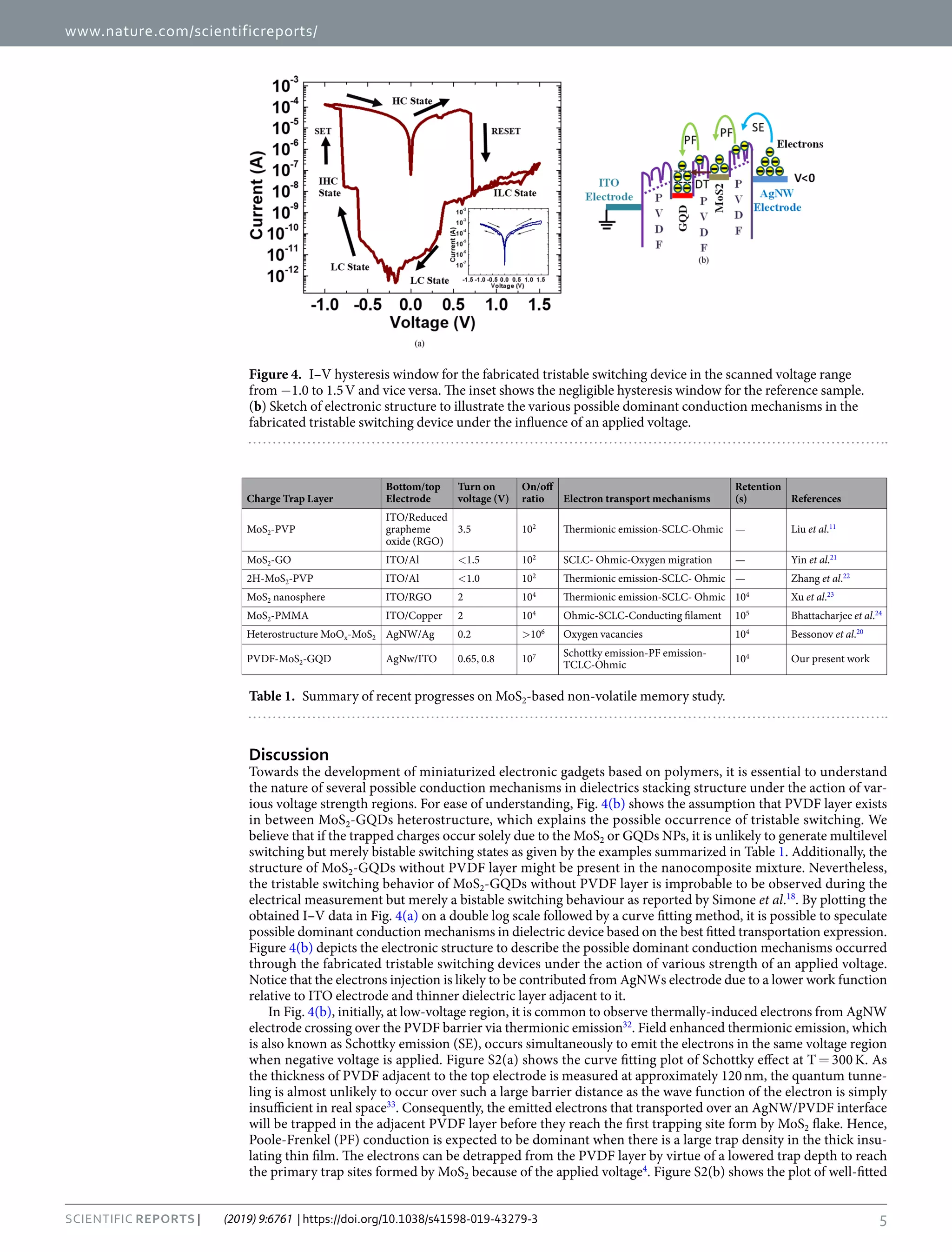
approximately 20% in comparison with the ITO/glass sample. Subsequently, current-voltage (I–V) characteristics
of tristable switching-devices were conducted to examine the tristable behaviour in the presence of GMP-NC layer
as shown in Fig. 4(a). It is assumed that the device is in a lowest-conductivity (LC) state before the voltage sweeps
as shown in Fig. 4(a). When the applied voltage is swept from 0 to −1.0 V on top of AgNWs electrode, the current
increases until the first abrupt rise at −0.6 V to bring the initial LC state to an intermediate high-conductivity
(IHC) state. As the voltage is further increased to −0.8 V, the device is switched to highest-conductivity (HC)
state at that subsequent current rise. The observation of more than one high-conductivity state during the SET
process inherents the presence of heterostructure due to the mixture of nanoparticles and flakes in the charge
trapping layer26
. The current is then maintained at HC state from −1.0 to 0 V. It is continued to be retained at HC
state when the power is off, indicating nonvolatility behavior of the device. After the zero-volt, as can be seen in
positive bias region in Fig. 4(a), the device can be RESET to lowest-conductivity (LC) state region by sweeping
the voltage from 0 to 1.5 V. Two abrupt current reductions are observed at 0.68 V and 0.4 V, respectively. The
device is primarily switched to intermediate low-conductivity (ILC) state at 0.68 V, and maintained at ILC state
when the voltage increases from 0.68 to 1.5 V and return to 0.68 V. Continuing to reduce the voltage from 0.68 V,
the device encounters another abrupt decrease in the current at 0.4 V and the reduced rate slows down at about
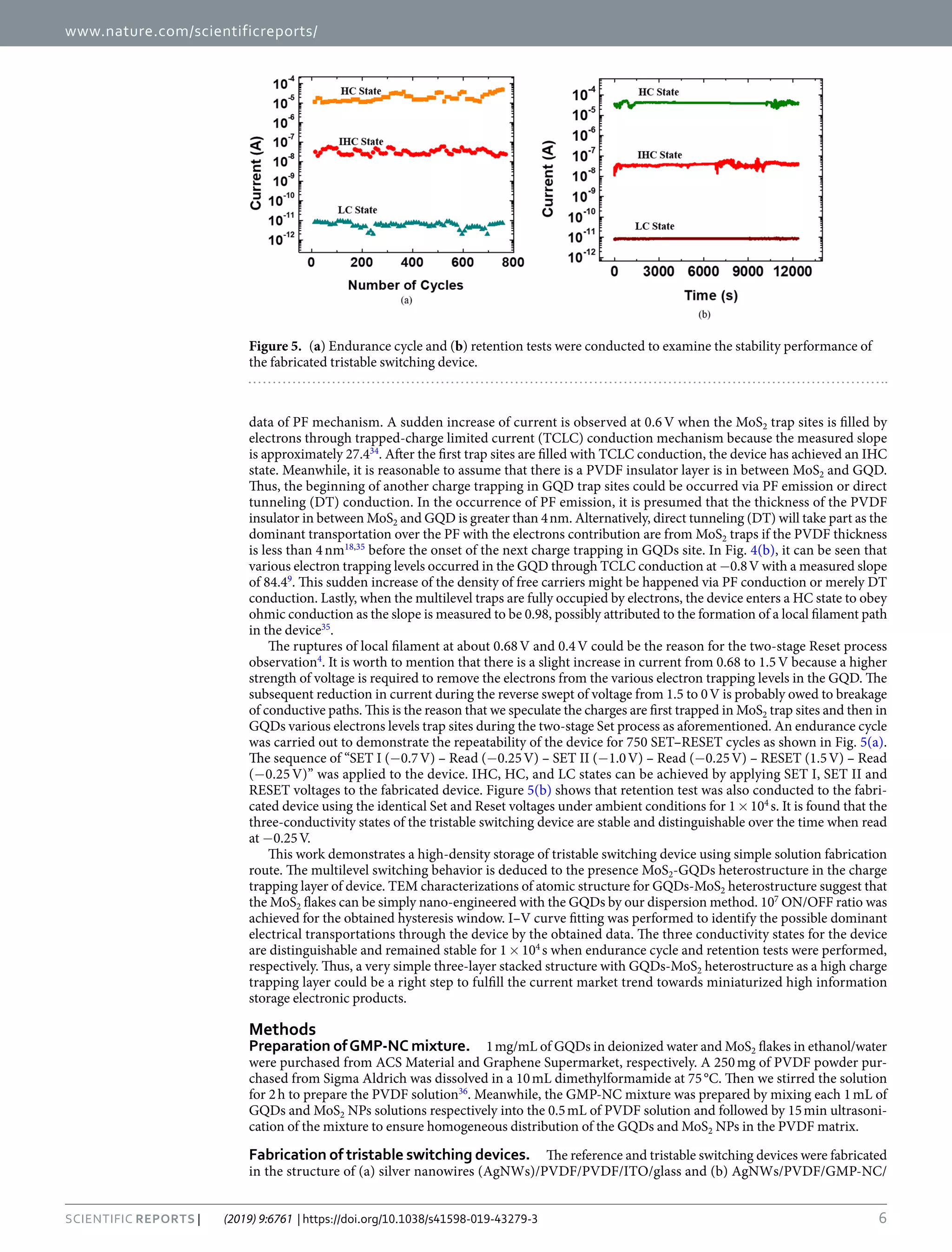
0.3 V and eventually returned to the LC state. The device demonstrates tristable switching behaviour as there
are two-stage of SET and RESET processes occur before the device reached its HC and LC states. The presence
of tristable switching memory window with high ON/OFF~107
in Fig. 4(a) could be strongly attributed to the
presence of MoS2-GQDs heterostructure in the tristable switching device as there is a negligible storage capability
for the reference device without the integration of both MoS2 and GQDs as shown in the inset. The higher den-
sity of the charge storage capability for the fabricated device is believed to be enhanced by the presence of GQDs
as it is not observed in the previous reported studies17,27–30
when only MoS2 flakes are introduced in the device
as summarized in Table 1. The large memory hysteresis window at low-voltage further proves that the GQD
enhances the charge storage capability because when the size of nanographene shrinks down to a few nm, there
Figure 1. (a) TEM image of the MoS2 flake decorated with GQDs. (b) TEM image of the GQDs on the MoS2.
(c) HR-TEM image of the GQDs on the few-layer MoS2. (d) Fourier filtered HR-TEM image of a single GQD/
MoS2 heterostructure on the selected yellow square area in (c), inset of (d) is the fast Fourier transform (FFT)
pattern displaying two sets of sixfold coordination symmetry corresponding to GQD (white) and MoS2 (yellow).
(e,f) HR-TEM images of the GQDs and few-layer MoS2. Two insets in (e,f) showing their corresponding FFT
patterns, respectively. (g,h) SAED images of the single-crystalline GQD and few-layer MoS2 observed along
the [001] zone axis. (i,j) Fourier filtered HR-TEM image of the GQD and few-layered MoS2 on the selected red
square area in (e,f). The dark spots indicating the void space. White and yellow lines representing the zigzag and
armchair directions, respectively. (k,l) Profile plots of grey scale intensities for the GQD and few-layer MoS2
along the selected line as illustrated in (I,j). Grey, cyan and yellow atoms denoting the C, Mo, and S elements,
respectively.](https://image.slidesharecdn.com/electricaltransportationmechanismsofmolybdenumdisulfideflakes-graphenequantumdotsheterostructureembe-211202061300/75/Electrical-transportation-mechanisms-of-molybdenum-disulfide-flakes-graphene-quantum-dots-heterostructure-embedded-in-polyvinylidene-fluoride-polymer-3-2048.jpg)


![[DevFest Strasbourg 2025] - NodeJs Can do that !!](https://cdn.slidesharecdn.com/ss_thumbnails/devfeststrasbourg2025-nodejscandothat-251127142731-da65b6fd-thumbnail.jpg?width=640&height=640&fit=bounds)
![[BDD 2025 - Full-Stack Development] Digital Accessibility: Why Developers nee...](https://cdn.slidesharecdn.com/ss_thumbnails/fs-digitalaccessibilitywhydevelopersneedtoknowandcarein2025-251127011019-0674441d-thumbnail.jpg?width=640&height=640&fit=bounds)


![[BDD 2025 - Artificial Intelligence] Building AI Systems That Users (and Comp...](https://cdn.slidesharecdn.com/ss_thumbnails/ai-buildingaisystemsthatusersandcompanieslove-251124030845-038f7732-thumbnail.jpg?width=640&height=640&fit=bounds)


![[BDD 2025 - Mobile Development] Exploring Apple’s On-Device FoundationModels](https://cdn.slidesharecdn.com/ss_thumbnails/md-exploringappleson-devicefoundationmodels-251124030840-d690542c-thumbnail.jpg?width=640&height=640&fit=bounds)


