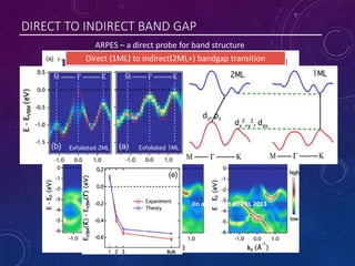
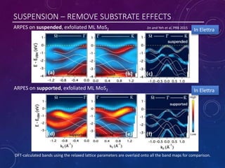
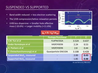
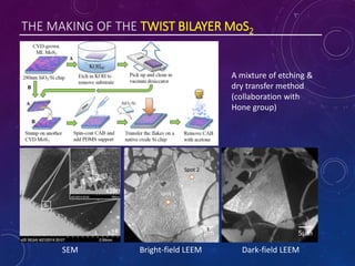
This document summarizes an ARPES and SPE-LEEM study on supported, suspended, and twisted bilayer MoS2. The study directly measures the MoS2 band structure using SPE-LEEM to study the band gap transition and role of interlayer coupling in monolayer, bilayer, and twisted bilayer MoS2. It also studies the substrate effect by examining suspended MoS2. Preliminary results on effective mass and spin-orbit splitting are also presented.
This research, presented at the 2014 APS March Meeting in Denver, Colorado, characterizes magnetic phase transitions in the manganese-doped dichalcogenide TaS2.
Copper (775) - an optics, 2PPE, and Bulk state simulation studyPo-Chun Yeh
My earlier studies on Cu(775) - a tilt cut highly crystalline copper surface using ultrafast femtosecond laser based 2-photon photoemission and its related simulation via Fortran 77.
Invited lecture of the Simposium N "Surface Engineering - functional coatings and modified surfaces" at the XIII SBPMat (Brazilian MRS) meeting, in João Pessoa (Brazil). The lecture took place on September 29th, 2014.
The speaker was Christopher Muratore, "Wright Brothers Institute Endowed Chair Professor" at the Department of Chemical and Materials Engineering from University of Dayton (USA).
Los días 22 y 23 de junio de 2016 organizamos en la Fundación Ramón Areces un simposio internacional sobre 'Materiales bidimensionales: explorando los límites de la física y la ingeniería'. En colaboración con el Massachusetts Institute of Technology (MIT), científicos de este prestigioso centro de investigación mostraron las propiedades únicas de materiales como el grafeno, de solo un átomo de espesor, y al mismo tiempo más resistente que el acero y mucho más ligero.
The driving engine for the exponential growth of digital information processing systems is scaling down the transistor dimensions. For decades, this has enhanced the device performance and density. However, the International Technology Roadmap for Semiconductors (ITRS) states the end of Moore’s law in the next decade due to the scaling challenges of silicon-based CMOS electronics, e.g. extremely high power density. The forward-looking solutions are the utilization of emerging materials and devices for integrated circuits, e.g. carbon-based materials. The presentation of my Ph.D. work focuses on graphene, one atomic layer of carbon sheet, experimentally discovered in 2004. Since fabrication technology of emerging materials is still in early stages, transistor modeling has been playing an important role for evaluating futuristic graphene-based devices and circuits. The device has been simulated by solving a quantum transport model based on non-equilibrium Green’s function (NEGF) approach, which fully treats short channel-length electrostatic effects and the quantum tunneling effects, leading to the technology exploration of graphene nanoribbon field effect transistors (GNR FETs) for the future. This research presents a comprehensive study of the width-dependence performance of the GNR FETs and the scaling of its channel length down to 2.5 nanometer, investigating its potential use beyond-CMOS emerging technology.
Flexible and Ultrasoft Inorganic 1D Semiconductor and Heterostructure Systems...Pawan Kumar
Low dimensionality and high flexibility are key demands for flexible electronic semiconductor devices. SnIP, the first atomic-scale double helical semiconductor combines structural anisotropy and robustness with exceptional electronic properties. The benefit of the double helix, combined with a diverse structure on the nanoscale, ranging from strong covalent bonding to weak van der Waals interactions, and the large structure and property anisotropy offer substantial potential for applications in energy conversion and water splitting. It represents the next logical step in downscaling the inorganic semiconductors from classical 3D systems, via 2D semiconductors like MXenes or transition metal dichalcogenides, to the first downsizeable, polymer-like atomic-scale 1D semiconductor SnIP. SnIP shows intriguing mechanical properties featuring a bulk modulus three times lower than any IV, III-V, or II-VI semiconductor. In situ bending tests substantiate that pure SnIP fibers can be bent without an effect on their bonding properties. Organic and inorganic hybrids are prepared illustrating that SnIP is a candidate to fabricate flexible 1D composites for energy conversion and water splitting applications. SnIP@C3N4 hybrid forms an unusual soft material core–shell topology with graphenic carbon nitride wrapping around SnIP. A 1D van der Waals heterostructure is formed capable of performing effective water splitting.
Report paper on Graphene Field Effect Transistor, for the Nanoelectronics course, in the Nanotechnology MSc program at the Information and Telecommunication (ICT) school KTH.
This presentation showcased first part of our work on graphene-based transistors as our final year project at NIT Patna under guidance of Prof.Wasim akram
Gamry’s eQCM 10M™ is a rapid, impedance-scanning electrochemical quartz crystal microbalance (EQCM) that adds a valuable tool in the analytical toolbox of anyone investigating interfacial processes.
Harvesting Hot Holes in Plasmon-Coupled Ultrathin Photoanodes for High-Perfor...Pawan Kumar
The harvesting of hot carriers produced by plasmon decay to generate electricity or drive a chemical reaction enables the reduction of the thermalization losses associated with supra-band gap photons in semiconductor photoelectrochemical (PEC) cells. Through the broadband harvesting of light, hot-carrier PEC devices also produce a sensitizing effect in heterojunctions with wide-band gap metal oxide semiconductors possessing good photostability and catalytic activity but poor absorption of visible wavelength photons. There are several reports of hot electrons in Au injected over the Schottky barrier into crystalline TiO2 and subsequently utilized to drive a chemical reaction but very few reports of hot hole harvesting. In this work, we demonstrate the efficient harvesting of hot holes in Au nanoparticles (Au NPs) covered with a thin layer of amorphous TiO2 (a-TiO2). Under AM1.5G 1 sun illumination, photoanodes consisting of a single layer of ∼50 nm diameter Au NPs coated with a 10 nm shell of a-TiO2 (Au@a-TiO2) generated 2.5 mA cm–2 of photocurrent in 1 M KOH under 0.6 V external bias, rising to 3.7 mA cm–2 in the presence of a hole scavenger (methanol). The quantum yield for hot-carrier-mediated photocurrent generation was estimated to be close to unity for high-energy photons (λ < 420 nm). Au@a-TiO2 photoelectrodes produced a small positive photocurrent of 0.1 mA cm–2 even at a bias of −0.6 V indicating extraction of hot holes even at a strong negative bias. These results together with density functional theory modeling and scanning Kelvin probe force microscope data indicate fast injection of hot holes from Au NPs into a-TiO2 and light harvesting performed near-exclusively by Au NPs. For comparison, Au NPs coated with a 10 nm shell of Al2O3 (Au@Al2O3) generated 0.02 mA cm–2 of photocurrent in 1 M KOH under 0.6 V external bias. These results underscore the critical role played by a-TiO2 in the extraction of holes in Au@a-TiO2 photoanodes, which is not replicated by an ordinary dielectric shell. It is also demonstrated here that an ultrathin photoanode (<100 nm in maximum thickness) can efficiently drive sunlight-driven water splitting.
A Front Surface Optimization Study for Photovoltaic ApplicationTELKOMNIKA JOURNAL
In this paper, we presented a possible front surface optical enhancement of Si solar cell by
optimizing the Antireflection (AR) and light trapping (LT) schemes. Conventional plasma enhanced
chemical vapor deposition (PECVD) and in house hot wire chemical vapor deposition (HWCVD) tool was
used to deposit Silicon Nitride (SiNX) layer and optimized at 668nm wavelength. This was followed by
surface texturing of random pyramids to further enhance the broadband reflectance of the front surface.
Broadband reflectance measurement using integrating sphere method showed achieved weighted average
reflectance (WAR) value of as low as 1.8% and 1.5%, when 85nm SiNX was deposited on top of random
pyramids structure using HWCVD and PECVD methods, respectively.
High impedance surface_his_ris_amc_nurmerical_analytical_analysis利 金
Features of an AMC such as dispersion diagram and reflection phase are discussed numerically and analytically, along with their experimental set up. Parametric study on polarization (TE and TM,substrate thickness and dielectric constant and unit cell size and spacing is carried out. Their design equations are included from different references.
the paper focuses on the fabrication and characterization of heterostructures using transition metal dichalcogenide (TMDC) monolayers. The authors describe the process of mechanical exfoliation to obtain thin flakes of TMDC material, which are then placed on a viscoelastic polydimethylsiloxane film. These monolayers are subsequently stamped onto a silicon wafer covered with thermal oxide to create heterobilayers .
The paper also discusses the use of ultrafast optical-pump/terahertz-probe near-field microscopy to study these heterostructures. The authors explain that this technique allows them to investigate the electric near fields and scattered fields of the emitted waveforms, as well as the photo-induced polarizability .
The experimental setup involves a high-average-power, low-noise Yb:YAG thin-disc oscillator, which generates terahertz probe pulses through optical rectification of 200-fs-long pulses. These pulses are centered at a wavelength of 1,030 nm and are generated in a gallium phosphide crystal .
The paper likely includes additional details on the experimental procedures, data analysis, and results obtained from the terahertz near-field microscopy experiments. It may also discuss the potential applications and implications of the findings
p-i-n Solar Cell Modeling with Graphene as ElectrodeWahiduzzaman Khan
Graphene is a 2-D atomic layer of carbon atoms with unique electronic properties like outstanding carrier mobility, high carrier saturation velocity, excellent thermal conductivity, high mechanical strength, transparency, thinness, and flexibility which make graphene an excellent choice of material for advanced applications in future solar cell design. We modeled a solar cell using graphene as the front electrode to study its performance and compare the performance with that of other possible contenders- indium tin oxide (ITO), widely used material at present and carbon nanotube (CNT), another promising material in this regard. Numerical solutions of the electrostatic and transport equations were obtained using the finite-element method. It was found that solar cell with graphene electrode can outperform the others. We also studied its performance as a function of various parameters. The developed model and obtained results are important for the design of solar cell with graphene as electrode.
Search and Society: Reimagining Information Access for Radical FuturesBhaskar Mitra
The field of Information retrieval (IR) is currently undergoing a transformative shift, at least partly due to the emerging applications of generative AI to information access. In this talk, we will deliberate on the sociotechnical implications of generative AI for information access. We will argue that there is both a critical necessity and an exciting opportunity for the IR community to re-center our research agendas on societal needs while dismantling the artificial separation between the work on fairness, accountability, transparency, and ethics in IR and the rest of IR research. Instead of adopting a reactionary strategy of trying to mitigate potential social harms from emerging technologies, the community should aim to proactively set the research agenda for the kinds of systems we should build inspired by diverse explicitly stated sociotechnical imaginaries. The sociotechnical imaginaries that underpin the design and development of information access technologies needs to be explicitly articulated, and we need to develop theories of change in context of these diverse perspectives. Our guiding future imaginaries must be informed by other academic fields, such as democratic theory and critical theory, and should be co-developed with social science scholars, legal scholars, civil rights and social justice activists, and artists, among others.
PHP Frameworks: I want to break free (IPC Berlin 2024)Ralf Eggert
In this presentation, we examine the challenges and limitations of relying too heavily on PHP frameworks in web development. We discuss the history of PHP and its frameworks to understand how this dependence has evolved. The focus will be on providing concrete tips and strategies to reduce reliance on these frameworks, based on real-world examples and practical considerations. The goal is to equip developers with the skills and knowledge to create more flexible and future-proof web applications. We'll explore the importance of maintaining autonomy in a rapidly changing tech landscape and how to make informed decisions in PHP development.
This talk is aimed at encouraging a more independent approach to using PHP frameworks, moving towards a more flexible and future-proof approach to PHP development.
Neuro-symbolic is not enough, we need neuro-*semantic*Frank van Harmelen
Neuro-symbolic (NeSy) AI is on the rise. However, simply machine learning on just any symbolic structure is not sufficient to really harvest the gains of NeSy. These will only be gained when the symbolic structures have an actual semantics. I give an operational definition of semantics as “predictable inference”.
All of this illustrated with link prediction over knowledge graphs, but the argument is general.
GDG Cloud Southlake #33: Boule & Rebala: Effective AppSec in SDLC using Deplo...James Anderson
Effective Application Security in Software Delivery lifecycle using Deployment Firewall and DBOM
The modern software delivery process (or the CI/CD process) includes many tools, distributed teams, open-source code, and cloud platforms. Constant focus on speed to release software to market, along with the traditional slow and manual security checks has caused gaps in continuous security as an important piece in the software supply chain. Today organizations feel more susceptible to external and internal cyber threats due to the vast attack surface in their applications supply chain and the lack of end-to-end governance and risk management.
The software team must secure its software delivery process to avoid vulnerability and security breaches. This needs to be achieved with existing tool chains and without extensive rework of the delivery processes. This talk will present strategies and techniques for providing visibility into the true risk of the existing vulnerabilities, preventing the introduction of security issues in the software, resolving vulnerabilities in production environments quickly, and capturing the deployment bill of materials (DBOM).
Speakers:
Bob Boule
Robert Boule is a technology enthusiast with PASSION for technology and making things work along with a knack for helping others understand how things work. He comes with around 20 years of solution engineering experience in application security, software continuous delivery, and SaaS platforms. He is known for his dynamic presentations in CI/CD and application security integrated in software delivery lifecycle.
Gopinath Rebala
Gopinath Rebala is the CTO of OpsMx, where he has overall responsibility for the machine learning and data processing architectures for Secure Software Delivery. Gopi also has a strong connection with our customers, leading design and architecture for strategic implementations. Gopi is a frequent speaker and well-known leader in continuous delivery and integrating security into software delivery.
Essentials of Automations: Optimizing FME Workflows with ParametersSafe Software
Are you looking to streamline your workflows and boost your projects’ efficiency? Do you find yourself searching for ways to add flexibility and control over your FME workflows? If so, you’re in the right place.
Join us for an insightful dive into the world of FME parameters, a critical element in optimizing workflow efficiency. This webinar marks the beginning of our three-part “Essentials of Automation” series. This first webinar is designed to equip you with the knowledge and skills to utilize parameters effectively: enhancing the flexibility, maintainability, and user control of your FME projects.
Here’s what you’ll gain:
- Essentials of FME Parameters: Understand the pivotal role of parameters, including Reader/Writer, Transformer, User, and FME Flow categories. Discover how they are the key to unlocking automation and optimization within your workflows.
- Practical Applications in FME Form: Delve into key user parameter types including choice, connections, and file URLs. Allow users to control how a workflow runs, making your workflows more reusable. Learn to import values and deliver the best user experience for your workflows while enhancing accuracy.
- Optimization Strategies in FME Flow: Explore the creation and strategic deployment of parameters in FME Flow, including the use of deployment and geometry parameters, to maximize workflow efficiency.
- Pro Tips for Success: Gain insights on parameterizing connections and leveraging new features like Conditional Visibility for clarity and simplicity.
We’ll wrap up with a glimpse into future webinars, followed by a Q&A session to address your specific questions surrounding this topic.
Don’t miss this opportunity to elevate your FME expertise and drive your projects to new heights of efficiency.
Dev Dives: Train smarter, not harder – active learning and UiPath LLMs for do...UiPathCommunity
💥 Speed, accuracy, and scaling – discover the superpowers of GenAI in action with UiPath Document Understanding and Communications Mining™:
See how to accelerate model training and optimize model performance with active learning
Learn about the latest enhancements to out-of-the-box document processing – with little to no training required
Get an exclusive demo of the new family of UiPath LLMs – GenAI models specialized for processing different types of documents and messages
This is a hands-on session specifically designed for automation developers and AI enthusiasts seeking to enhance their knowledge in leveraging the latest intelligent document processing capabilities offered by UiPath.
Speakers:
👨🏫 Andras Palfi, Senior Product Manager, UiPath
👩🏫 Lenka Dulovicova, Product Program Manager, UiPath
Transcript: Selling digital books in 2024: Insights from industry leaders - T...BookNet Canada
The publishing industry has been selling digital audiobooks and ebooks for over a decade and has found its groove. What’s changed? What has stayed the same? Where do we go from here? Join a group of leading sales peers from across the industry for a conversation about the lessons learned since the popularization of digital books, best practices, digital book supply chain management, and more.
Link to video recording: https://bnctechforum.ca/sessions/selling-digital-books-in-2024-insights-from-industry-leaders/
Presented by BookNet Canada on May 28, 2024, with support from the Department of Canadian Heritage.
Let's dive deeper into the world of ODC! Ricardo Alves (OutSystems) will join us to tell all about the new Data Fabric. After that, Sezen de Bruijn (OutSystems) will get into the details on how to best design a sturdy architecture within ODC.
Kubernetes & AI - Beauty and the Beast !?! @KCD Istanbul 2024Tobias Schneck
As AI technology is pushing into IT I was wondering myself, as an “infrastructure container kubernetes guy”, how get this fancy AI technology get managed from an infrastructure operational view? Is it possible to apply our lovely cloud native principals as well? What benefit’s both technologies could bring to each other?
Let me take this questions and provide you a short journey through existing deployment models and use cases for AI software. On practical examples, we discuss what cloud/on-premise strategy we may need for applying it to our own infrastructure to get it to work from an enterprise perspective. I want to give an overview about infrastructure requirements and technologies, what could be beneficial or limiting your AI use cases in an enterprise environment. An interactive Demo will give you some insides, what approaches I got already working for real.
Kubernetes & AI - Beauty and the Beast !?! @KCD Istanbul 2024
APS march meeting 2015
1. ARPES and SPE-LEEM Study on
Supported, Suspended, and
Twisted Bilayer MoS2
SPEAKER: PO-CHUN(FIGO) YEH
ADVISOR: PROF. R. M. OSGOOD
“SPE-LEEM” = Spectroscopic Photo-Emission and Low
Energy Electron Microscopy
1
APS March meeting 2015 Y2: Focus Session: Beyond Graphene - New 2D Materials
2. MANY THANKS!
Jurek Sadowski
DaTong Zhang
Arend van der Zande
Abdullah Al-Mahboob
Prof. James Hone
Prof. Irving Herman
Daniel A. ChenetProf. R. M. Osgood
WenCan Jin
Jerry Dadap
Nader Zaki Peter Sutter
2
Ghidewon Arefe
Andrea Locatelli Tevfik Onur Metnes Alessandro Sala
and many!
3. WHY WE WANT TO STUDY THIS?
• Spin-orbit coupling
• It has a bandgap! • Photoluminescence (PL)
• Twisted Bilayer MoS2
Strong PL in monolayer MoS2
Nano. Lett. 10, 1271-1275 (2010)
High quantum efficiency
1000 times stronger PL in ML
WS2, WSe2 than in bulk
ACS Nano 7 (1), 791–797 (2013)
Direct bandgap in ML
Thin, flexible devices
E.g. Li-ion battery and transistors
Nano Lett., 11 (9), pp 3768–
3773 (2011)
Chem. Commun. , 47,
4252-4254 (2011)
Enhanced spin lifetimes
Large spin Hall angles
VBM S-O splitting up to 456meV in WSe2
PRB 84, 153402 (2011)
Nano Lett. 13 (7), pp 3106–3110 (2013)
van der Zande et al, Nano. Lett. 14, 2014
Liu et al, Nat. Commun. 5, 2014
Huang et al, Nano Lett 14, 2014
A lot of PL and Raman studies!
4. OUR AIM:
With SPE-LEEM, we can:
o Measure the MoS2 band structure directly
o Study the band gap transition and the role of interlayer
coupling in ML, BL, and twist bilayer MoS2
o Study the substrate effect via suspension
o Study hole effective mass directly
5. WHY SPE-LEEM?
Micron-size spot, Direct band structure, fast real time imaging, large area mapping,
UHV, surface doping, depth profile.
NSLS I Nanospectroscopy
1. mLEED – reciprocal space mapping: surface crystalline
2. LEEM – real space mapping: surface corrugation
3. mARPES – band structure mapping
4. PEEM and XPEEM(ELETTRA) – chemical sensitivity,
ionization, core level orbitals, surface composition
BNL, NY, USA Elettra, Trieste, Italy
5
2 µm
LEEM, ML graphene
6. DIRECT TO INDIRECT BAND GAP
Photoelectron k-space
mapping
Direct (1ML) to indirect(2ML+) bandgap transition
ARPES – a direct probe for band structure
Jin and Yeh et al, PRL 2013
dz, pz
dx
2
+y
2, dxy
7. SUSPENSION – REMOVE SUBSTRATE EFFECTS
DFT-calculated bands using the relaxed lattice parameters are overlaid onto all the band maps for comparison.
ARPES on suspended, exfoliated ML MoS2
ARPES on supported, exfoliated ML MoS2 In Elettra
In ElettraJin and Yeh et al, PRB 2015
8. • Band width reduced -> less electron scattering
• The UVB compression/lattice relaxation persists
• UVB less dispersive -> Smaller hole effective
mass (-10.6%) -> Larger mobility (+11.6%)
SUSPENDED VS SUPPORTED
µh = h · th/ meff
Jin and Yeh et al, PRB 2015
Package/functional Γ Κ
S.W. Yun et al FLAPW/GGA 3.524 0.637
Andor Kormányos et al VASP/HSE06 2.24 0.53
H. Peelaers et al VASP/HSE06 2.8 0.44
T. Cheiwchanchamnangij et al Quasiparticle GW/LDA 3.108 0.428
Suspended MoS2, measured - 2.00 0.43
Supported MoS2, measured - 1.85 0.48
9. THE MAKING OF THE TWIST BILAYER MoS2
A mixture of etching &
dry transfer method
(collaboration with
Hone group)
SEM Bright-field LEEM Dark-field LEEM
11. ANGLE–DEPENDENT BANDGAP OPENING
• Since K is invariant to twist angle and CB is almost intact, bandgap opening can
be derived from energy difference between Γ and K from UVB
• When twist angle reaches ~30°, the bandgap reaches its maximum (+200meV)
• The energy difference within each angle is larger than predicted (+70meV)
• Measured data shows asymmetry between 0° and 60° data as predicted
• Agrees well with PL and DFT calculations
Interlayer Spacing vs EK - EГ
d60 = 6.23Å
van der Zande et al, Nano. Lett. 14, 2014
Liu et al, Nat. Commun. 5, 2014
Align with the ~60 ° data point
Theoretical calculation Experimental data
70meV
12. EFFECTIVE MASS On going
Effective mass at K
via DFT calculation
Huang et al, Nano Lett 14, 2014
(Work in progress) Effective mass at Γ and K
-24% in meff, hole
13. CONCLUSION
Bandgap transition originates from the shifting of Γ at the
top-most valence band by quantum confinement
Hole effective mass / mobility affected by the substrate
Twist angle -> Interlayer coupling changes the band gap
SPE-LEEM system with LEEM, µLEED, and µARPES is ideal
for studying 2D materials
13
14. SPIN-ORBIT SPLITTING
• Predicted large s-o splitting at vicinity of K in ML MoS2
• Possible causes of broadening:
• a decrease in the quasi-particle lifetime
• a splitting of the spin degenerate band into two bands due to spin-orbit coupling.
Theory vs Suspended: 148 meV vs 78±19 meV
On going
Jin and Yeh et al, PRB 2015
ML MoSe2, splitting~180eV
ARPES with MBE growth in UHV
Zhang et al, Nat Nanotech 9, 2014
17. SPE-LEEM - PERSPECTIVES
ELMITEC SPLEEM
Energy Analyzer
Manipulator.
Grounded.
(High voltage @
2kV)
Preparation
chambers
Photon energy: 15-150eV
Good energy resolution: 100meV
Good spatial resolution: 8nm
Large mapping area: FOV = 100µm
Thermal coupler
Sample holder
d ~ 10mm
17
18. NOTES
• Work function in ML: 1.85eV; bilayer 1+ eV; highly doped, lower bound of the
bandgap.
• Other ways of change lattice constant – strain: up to 2.2% (Nano Lett., 2013, 13 (8)
• LEED on suspended MoS2? Should be better. But we did not have the chance to do
the measurement.
• Error bars: average of the all six high sym directions + resolution limit of the
apparatus +
• Fitting the entire bands using tight binding theory instead of locally? To get a
better fit for peak, etc.
Mo dx2+dy2, dxy Mo dxy, dyz Mo d3z2-r2 S pxy S pz
Cappelluti et al, PRB 88, 2013
19. EFFECTIVE MASS AT K POINT
a: experimental lattices, ref Phys. Rev. B 85 (2012). b: optimized lattices from calculation
Hole effective mass agrees well with the calculations, for both 1ML and 2ML
19
Thickness Electron Mass Hole Mass Method Reference
Lattice
Constant
ML N/A 0.52 ABINIT/ GGA Our results. 3.28
ML N/A 0.48 Experiment Our results. 3.28
ML 0.53 0.52 DFT-GW-BSE
A. Ramasubramanim,
PRB 2012 3.32
ML 0.29a/0.26b 0.34a/0.33b DFT-GW-BSE
Hongliang Shi, PRB
2013 3.286
ML 0.19 0.4 FLAPW-GGA W. S. Yun. PRB 2012 3.286
2ML N/A 0.432 Experiment Our results. 3.28
2ML 0.3 0.49 LDA A. Kumar, EPJB 2012 3.282
2ML 0.3 0.3 FLAPW-GGA W. S. Yun. PRB 2012 3.286
20. Foldable FETs and solar cells.
Goal toward printable solar cell on
a sheet of paper (gr as an example)Flash memory
EXAMPLES OF APPLICATIONS
21. Constant energy plane near EF
The band near EF originates from
Mo 4dz
2 orbital and S 3Pz orbital,
where Mo 4d character is
dominant by a factor of ~3.
Consider only the d orbital:
Two cuts along high symmetric direction in BZ
Selection rules in ARPES
• Fermi’s golden rule:
• Hamiltonian
• Matrix elements
The final state can be
approximated by a plane wave;
the initial state represents the
wave function of the electrons
in solid.
Our calculation and analysis
22. July 27, 2015
Slide 22
Many-body Physics from ARPES
Response of crystal to “hole”
ARPES measures Spectral Function A(k,w)
Band renormalization Re[S(k,w)]
Scattering Rate Im[S(k,w)]
Re[S(k,w)] and Im[S(k,w)] related by
Kramers-Kronig transformation
27. LATTICE RELAXATION
• Up-most valence band (UVB) compression:
(UVBmax-UVBmin)experiment/ (UVBmax-UVBmin)theory
• The compression rate of ML MoS2 is 80% in exfoliated and 50% in CVD;
• Relaxation: ~3.6% lateral lattice expansion in ML MoS2 compared to bulk;
lattice constant a = 3.28±0.10 Å vs 3.16 Å (-2% in c /z axis)
• Larger hole effective mass -> lower hole mobility µh = h · th/ meff
ML MoS2 UVB and calculations: Si supported and free standing