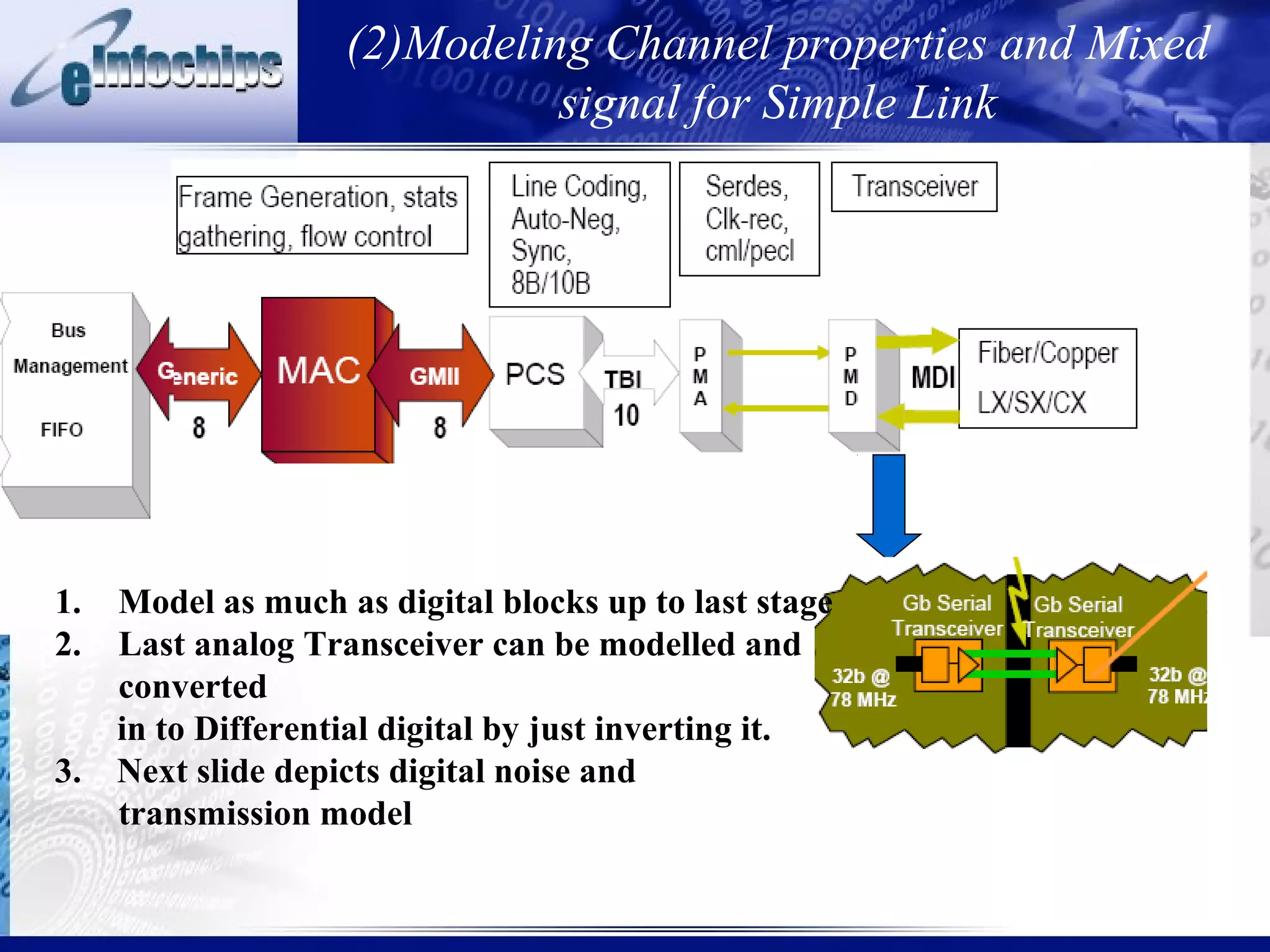
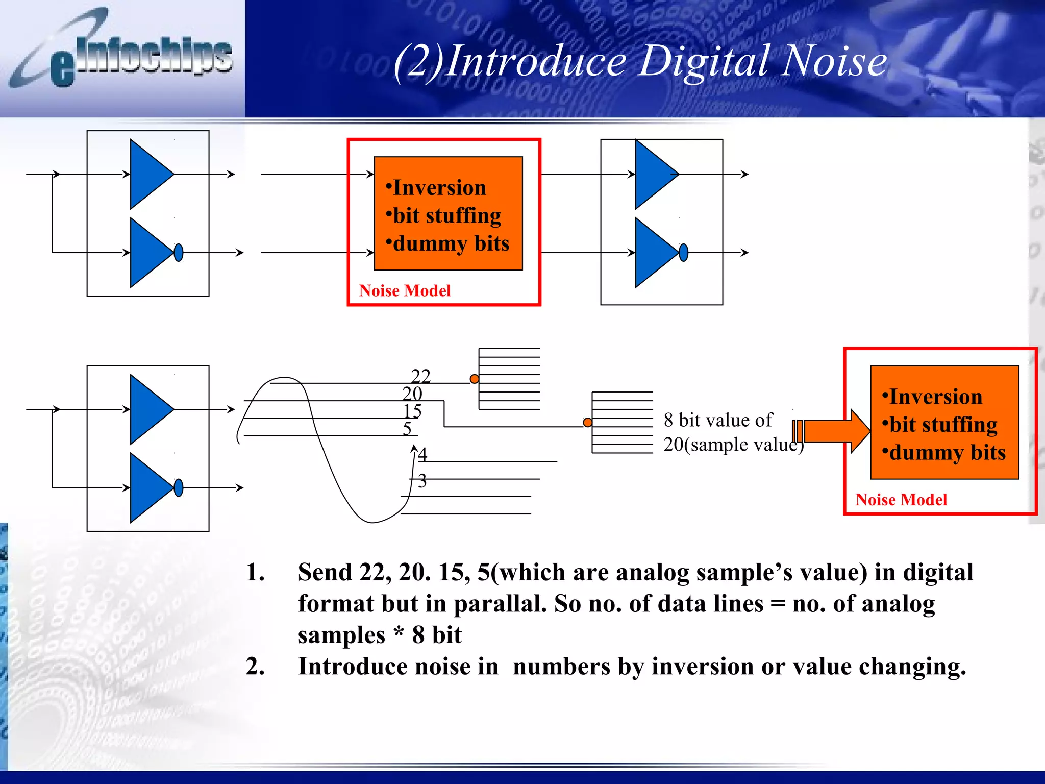
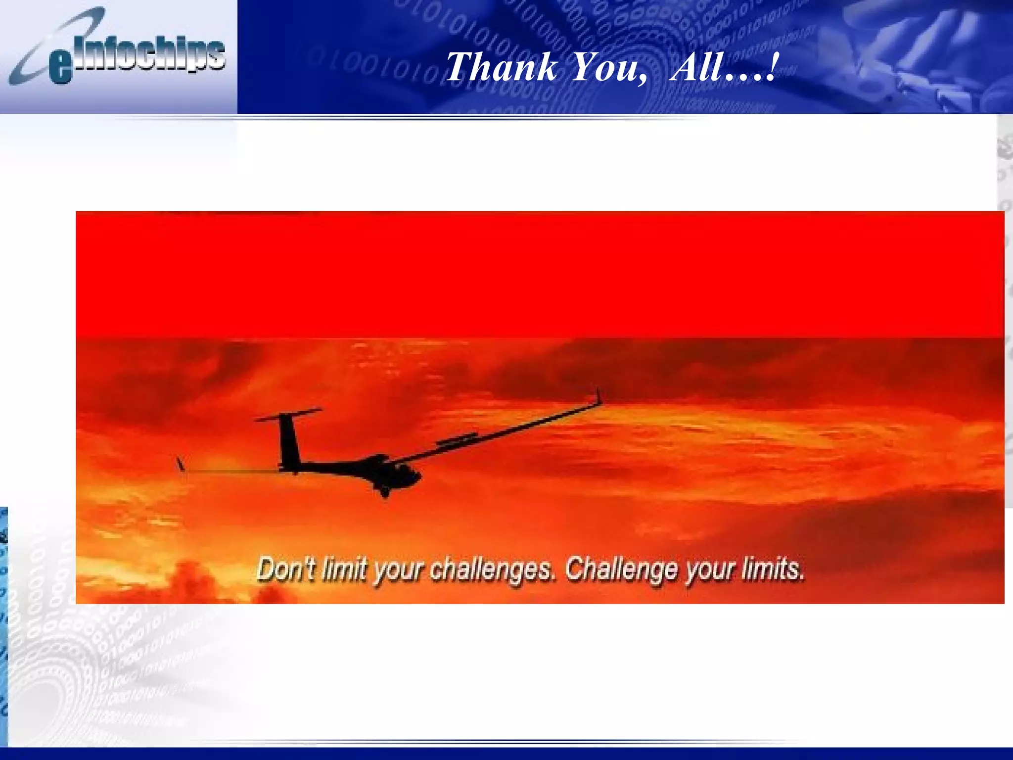
This document discusses modeling system behaviors and properties. It addresses:
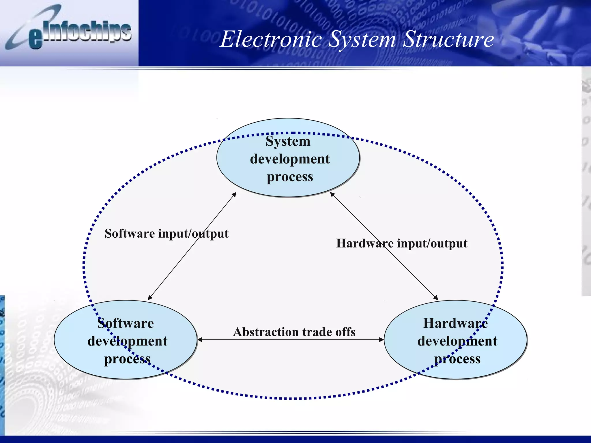
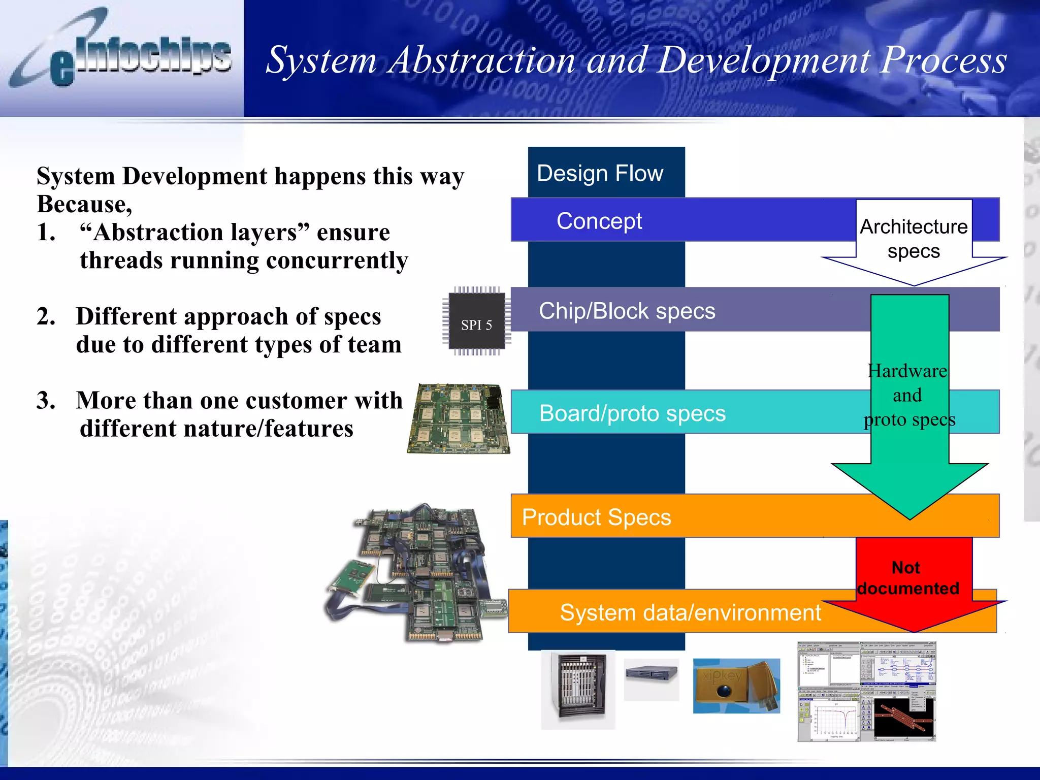
1) System development involves different abstraction layers to allow concurrent work between software and hardware teams with different inputs and outputs.
2) Modeling must account for multiple customers with varying requirements.
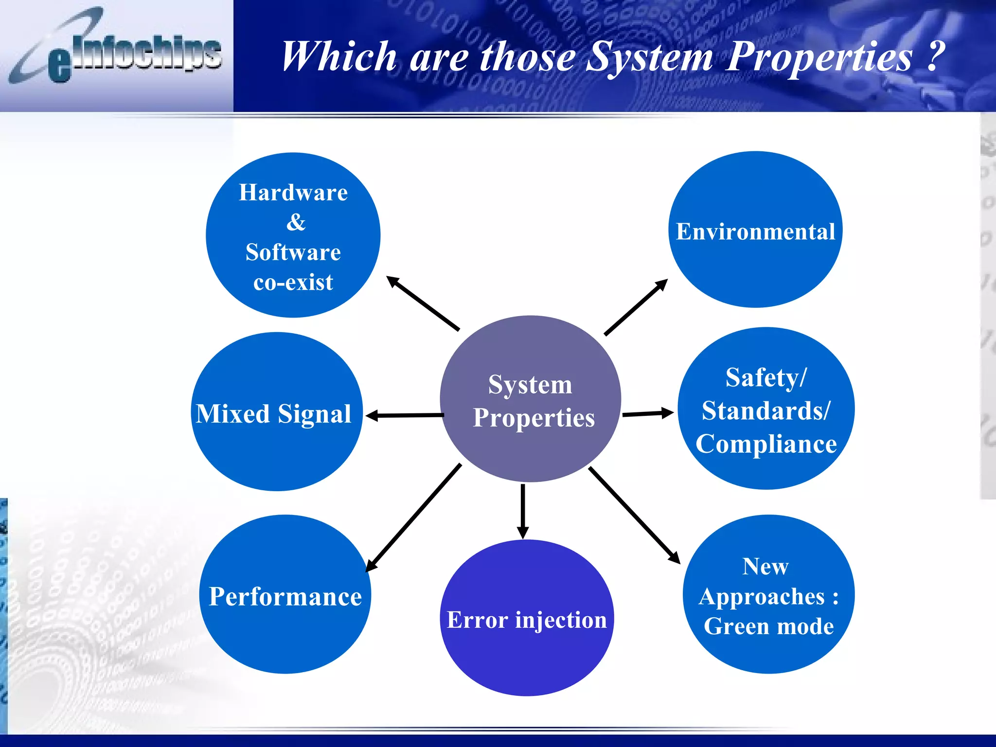
3) Important system properties to model include mixed signal behavior, safety standards, performance, and error injection.


![Vibe Coding vs. Spec-Driven Development [Free Meetup]](https://cdn.slidesharecdn.com/ss_thumbnails/vibecodingvsspecdrivendevelopment-251209105622-43f455e7-thumbnail.jpg?width=640&height=640&fit=bounds)


