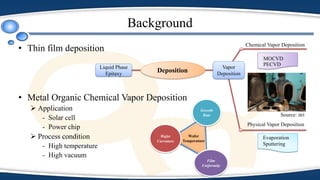
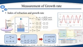
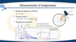
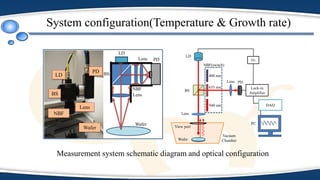
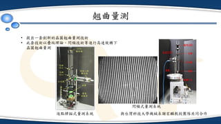
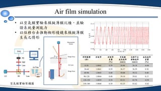
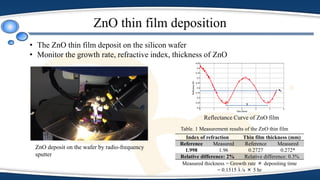
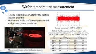
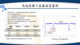
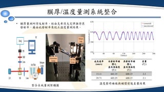
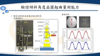
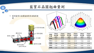
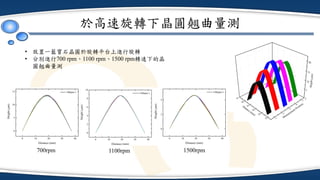
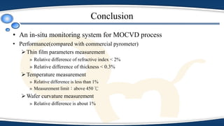
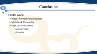
MOCVD半導體製程即時監控系統
Speaker: Ju-Yi Lee
Department of Mechanical Engineering, National Central University, Taiwan.
Outline
1. Introduction
2. Principle
3. System configuration
4. Experiments & Results
5. Conclusion
INTRODUCTION
Background
Literatures review
Commercial products
Purpose
紅豆餅
Background
• Thin film deposition
• Metal Organic Chemical Vapor Deposition
 Application
- Solar cell
- Power chip
 Process condition
- High temperature
- High vacuum
Deposition
Chemical Vapor Deposition
MOCVD
PECVD
Physical Vapor Deposition
Evaporation
Sputtering
Vapor
Deposition
Liquid Phase
Epitaxy
Wafer
Curvature
Growth
Rate
Film
Uniformity
Wafer
Temperature
Source: itri
Literatures review (Growth rate & Temperature)
• Thin film growth rate measurement
 Quartz crystal microbalance
a
 Reflectance interferometry
b
• Temperature measurement
 Two-color and Multi-wavelength pyrometry
c
a: C. S. Lu and O. Lewis, “Investigation of film ‐ thickness determination by oscillating quartz
resonators with large mass load”, 1972.
b: J.A. Dobrowolski, “Optical Properties of Thin Films and Coating” Chap.42 of Handbook of Optics,
McGraw-Hill, Inc, 1995.
c: B. Müller, U. Renz, “Development of a fast fiber-optic two-color pyrometer for the temperature
measurement of surfaces with varying emissivities”, Review of Scientific Instruments, 2001.
Source: ADVANTEST
Source: c
Literatures review (Temperature on surface)
• Wafer materials:Si, Sapphire, SiC, etc.
• GaN/InGaN layer measurement
Material transmittance
400 nm wavelength
No Fabry-Pérot interferometer
Literatures review (Wafer curvature)
• LayTec EpiCurveTT:
 Curvature range: -7000 km-1(convex) to +800 km-1(concave)
 Aspherical bowing curvature measurements with an
Advanced Resolution option
Source:LayTec
Commercial products
• FRT, kSA, LayTec, etc.
• The accuracy of equipment:
e.g., LayTec EpiTT
» Typical growth rate accuracy better than ±1%
» Typical wafer temperature accuracy better than ±1℃
Purpose
• Monitor of wafer parameters
Growth rate & Temperature monitoring devices
Enhance quality
Cost down
Source: LayTec
PRINCIPLE
Measurement of Growth rate
Blackbody Radiation Theorem
Measurement of Temperature
Curvature measurement
Measurement of Growth rate
• Index of refraction and growth rate
  nfsolven 
nTn
w
G
24




nGw

4

sL RRR  0
T
w
2

2
2
2
0
2
0
)(
)(
)(
)(
s
s
L
nn
nn
nn
nn
R






             021214214122f(n)
222234
 LsssLssssLsLL RnnnnRnnnnnRnnRnR
)cos(21
)cos(2
00
002


ss
ss
RRRR
RRRR
rR



nGtnd





22

Substrate
Light Ii
Reflected
Light Io
2
22
2
2
0
2
0
2
0
02
00
)(
)(
)(
)(
s
s
s
s
ss
nn
nn
NN
NN
rR
nn
nn
NN
NN
rR












Blackbody Radiation Theorem
0 1000 2000 3000 4000 5000 6000 7000
0
5
10
15
20
25
30
600℃
700℃
800℃
900℃
1000℃
1100℃
1200℃
(nm)
E
b
(Wm-2
sr-1
nm-1
)
• Planck’s law
 
1
1
,
2
5
1


T
cb
e
c
TE



• Kirchhoff’s law
• Real-body radiation
   TETE breal ,,  



 1
  1
1c
2c
: Planck’s first constant
: Planck’s second constant


: Absorption
: Reflectance
 : Transmittance
 : Emissivity
Measurement of temperature
• Opaque & Specular substrate
1
T
=
1
Tcal
-
l
c2
ln
s
scal
R 1
• Temperature equation
• Thermal signal
s = C0 eEb = C0 e
c1
l5
exp -
c2
lT
æ
è
ç
ö
ø
÷
r
A
r

s
Filter
Detector
0C : System constant
cal: Calibration parameter
PD
PC
DAQ
NBF(switch)
Lens
Lens
BS
LD
Lock-in
Amplifier
Wafer
View port
Vacuum
Chamber
FG
System configuration(Temperature & Growth rate)
Lens
Lens
BS
NBF
Wafer
LD
LD
Lens
PD
NBF
BS
Wafer
PD
Measurement system schematic diagram and optical configuration
400 nm
635 nm
940 nm
翹曲量測
• 提出一套創新的晶圓翹曲量測技術
• 此套技術以疊紋理論、閃頻技術等進行高速旋轉下
晶圓翹曲量測
與台灣科技大學機械系謝宏麟教授團隊共同合作逐點掃描式量測系統
閃頻式量測系統
EXPERIMENTS & RESULTS
Air film simulation
• 以空氣膜實驗來模擬薄膜沉積,並驗
證系統量測能力
• 以位移台去推動楔形稜鏡來模擬薄膜
生長之情形
時間範圍
(秒)
折射率 折射率
差量
(%)
空氣膜
成長速率
(nm/s)
位移平台
移動速率
(nm/s)
成長速率
差量
(%)
0-30 1.0042 0.39 26.06 26.18 -0.46
30-60 1.0041 0.39 26.37 26.29 0.30
60-90 1.0045 0.40 59.08 59.32 0.40
90-120 1.0044 0.40 59.10 59.01 0.15
120-150 1.0039 0.39 83.21 83.70 -0.58
150-180 1.0040 0.39 83.25 83.62 -0.42空氣膜實驗架構圖
ZnO thin film deposition
Index of refraction Thin film thickness (mm)
Reference Measured Reference Measured
1.998 1.96 0.2727 0.272*
Relative difference: 2% Relative difference: 0.3%
Table. 1 Measurement results of the ZnO thin film
Measured thickness = Growth rate × depositing time
= 0.1515 Å /s × 5 hr
• The ZnO thin film deposit on the silicon wafer
• Monitor the growth rate, refractive index, thickness of ZnO
ZnO deposit on the wafer by radio-frequency
sputter
Reflectance Curve of ZnO film
Wafer temperature measurement
CP 400 nm 940 nm
(a). (b). (b)-(a) (c). (c)-(a)
455.4 450.5 -4.9 456.5 1.1
542.1 540.4 -2.3 541.3 -0.8
615.5 615.1 -0.4 615.7 0.2
701.7 702.0 0.3 701.8 0.1
781.6 780.8 -0.8 781.2 -0.4
858.5 858.6 0.1 858.6 0.1
943.0 943.2 0.2 943.1 0.1
Table. 2 The Measurement results and compare with
commercial pyrometer, (a) measured by commercial pyrometer,
CP, (b) by 400 nm NBF, and (c) by 940 nm NBF. (unit: °C).
Measurement system set on the heating chamber
600 650 700 750 800 850 900 950 1000
-3
-2
-1
0
1
2
3
Time(s)
Temperature(℃)
System resolution:0.67 ℃ at 580 ℃
• Heating single silicon wafer by the heating
vacuum chamber
• Monitor the wafer surface temperature and
analysis the system resolution
高速旋轉下晶圓溫度量測
0 0.06 0.12 0.18 0.24 0.3 0.36 0.42 0.48 0.54 0.6
500
520
540
560
580
600
620
640
660
Time(s)
Temperature(?)
PMT-200rpm
轉速/
光偵測器
200rpm 400rpm 800rpm
PDA 0.42℃ 0.46℃ 0.56℃
APD -0.58℃ -1℃ 0.48℃
PMT -0.24℃ -0.56℃ 0.2℃
與靜止時量測矽晶圓溫度(550.1℃)差量 於200rpm下資料擷取圖形
晶圓
載盤
• 因製程需求,晶圓在製程時需要以旋轉來達
到良好的薄膜均勻性
• 將一矽晶圓放置於加熱腔體,待加熱穩定後,
進行不同轉速的驗證系統
• 接收940 nm波段熱輻射來進行量測
• 400 nm波段之熱輻射訊號太弱,再進行旋轉
量測時無法解析
膜厚/溫度量測系統整合
成長速率
(nm/s)
未發射率補
償之
直流項溫度
(℃)
具發射率補
償之
直流項溫度
(℃)
差量
(℃)
13.11 602.35 600.15 2.2
29.71 602.25 600.15 2.1
• 膜厚量測所得反射率,經由克希荷夫定律推得其
發射率,藉由此發射率來校正溫度量測結果。
整合系統量測架構圖
溫度歷時曲線與補償前後差量結果
驗證傾斜角度晶圓翹曲量測能力
• 驗證本量測系統具備全域式傾斜角
度量測能力
量測結果:
藍寶石晶圓翹曲量測
• 量測藍寶石晶圓翹曲與表面輪廓重
建
量測
位置
10mm
高度值
(μm)
15mm
高度值
(μm)
20mm
高度值
(μm)
25mm
高度值
(μm)
30mm
高度值
(μm)
35mm
高度值
(μm)
1(黑) 3.67 6.28 8.30 8.21 6.13 3.28
2(紅) 5.21 8.01 9.84 9.75 7.52 4.48
3(藍) 7.04 9.94 12.11 11.42 9.31 6.29
4(粉) 5.58 8.74 11.42 10.61 8.03 4.74
5(綠) 4.45 7.64 9.32 8.82 6.34 3.12
pitch:100 μm
於高速旋轉下晶圓翹曲量測
• 放置一藍寶石晶圓於旋轉平台上進行旋轉
• 分別進行700 rpm、1100 rpm、1500 rpm轉速下的晶
圓翹曲量測
700rpm 1100rpm 1500rpm
Conclusion
• An in-situ monitoring system for MOCVD process
• Performance(compared with commercial pyrometer)
Thin film parameters measurement
» Relative difference of refractive index < 2%
» Relative difference of thickness < 0.3%
Temperature measurement
» Relative difference is less than 1%
» Measurement limit:above 450 ℃
Wafer curvature measurement
» Relative difference is about 1%
Conclusion
• Future works
Improve dynamic measurement
Modular & Compatible
High quality hardware
- Cooling system
- Low noise
Thank you for your listening
Acknowledge: This research was supported by the
Ministry of Science and Technology, Taiwan
(MOST 104-2218-E-008-002)

MOCVD半導體製程即時監控系統

  • 1.
    MOCVD半導體製程即時監控系統 Speaker: Ju-Yi Lee Departmentof Mechanical Engineering, National Central University, Taiwan.
  • 2.
    Outline 1. Introduction 2. Principle 3.System configuration 4. Experiments & Results 5. Conclusion
  • 3.
  • 4.
  • 5.
    Background • Thin filmdeposition • Metal Organic Chemical Vapor Deposition  Application - Solar cell - Power chip  Process condition - High temperature - High vacuum Deposition Chemical Vapor Deposition MOCVD PECVD Physical Vapor Deposition Evaporation Sputtering Vapor Deposition Liquid Phase Epitaxy Wafer Curvature Growth Rate Film Uniformity Wafer Temperature Source: itri
  • 6.
    Literatures review (Growthrate & Temperature) • Thin film growth rate measurement  Quartz crystal microbalance a  Reflectance interferometry b • Temperature measurement  Two-color and Multi-wavelength pyrometry c a: C. S. Lu and O. Lewis, “Investigation of film ‐ thickness determination by oscillating quartz resonators with large mass load”, 1972. b: J.A. Dobrowolski, “Optical Properties of Thin Films and Coating” Chap.42 of Handbook of Optics, McGraw-Hill, Inc, 1995. c: B. Müller, U. Renz, “Development of a fast fiber-optic two-color pyrometer for the temperature measurement of surfaces with varying emissivities”, Review of Scientific Instruments, 2001. Source: ADVANTEST Source: c
  • 7.
    Literatures review (Temperatureon surface) • Wafer materials:Si, Sapphire, SiC, etc. • GaN/InGaN layer measurement Material transmittance 400 nm wavelength No Fabry-Pérot interferometer
  • 8.
    Literatures review (Wafercurvature) • LayTec EpiCurveTT:  Curvature range: -7000 km-1(convex) to +800 km-1(concave)  Aspherical bowing curvature measurements with an Advanced Resolution option Source:LayTec
  • 9.
    Commercial products • FRT,kSA, LayTec, etc. • The accuracy of equipment: e.g., LayTec EpiTT » Typical growth rate accuracy better than ±1% » Typical wafer temperature accuracy better than ±1℃
  • 10.
    Purpose • Monitor ofwafer parameters Growth rate & Temperature monitoring devices Enhance quality Cost down Source: LayTec
  • 11.
    PRINCIPLE Measurement of Growthrate Blackbody Radiation Theorem Measurement of Temperature Curvature measurement
  • 12.
    Measurement of Growthrate • Index of refraction and growth rate   nfsolven  nTn w G 24     nGw  4  sL RRR  0 T w 2  2 2 2 0 2 0 )( )( )( )( s s L nn nn nn nn R                    021214214122f(n) 222234  LsssLssssLsLL RnnnnRnnnnnRnnRnR )cos(21 )cos(2 00 002   ss ss RRRR RRRR rR    nGtnd      22  Substrate Light Ii Reflected Light Io 2 22 2 2 0 2 0 2 0 02 00 )( )( )( )( s s s s ss nn nn NN NN rR nn nn NN NN rR            
  • 13.
    Blackbody Radiation Theorem 01000 2000 3000 4000 5000 6000 7000 0 5 10 15 20 25 30 600℃ 700℃ 800℃ 900℃ 1000℃ 1100℃ 1200℃ (nm) E b (Wm-2 sr-1 nm-1 ) • Planck’s law   1 1 , 2 5 1   T cb e c TE    • Kirchhoff’s law • Real-body radiation    TETE breal ,,       1   1 1c 2c : Planck’s first constant : Planck’s second constant   : Absorption : Reflectance  : Transmittance  : Emissivity
  • 14.
    Measurement of temperature •Opaque & Specular substrate 1 T = 1 Tcal - l c2 ln s scal R 1 • Temperature equation • Thermal signal s = C0 eEb = C0 e c1 l5 exp - c2 lT æ è ç ö ø ÷ r A r  s Filter Detector 0C : System constant cal: Calibration parameter
  • 15.
    PD PC DAQ NBF(switch) Lens Lens BS LD Lock-in Amplifier Wafer View port Vacuum Chamber FG System configuration(Temperature& Growth rate) Lens Lens BS NBF Wafer LD LD Lens PD NBF BS Wafer PD Measurement system schematic diagram and optical configuration 400 nm 635 nm 940 nm
  • 16.
  • 17.
  • 18.
    Air film simulation •以空氣膜實驗來模擬薄膜沉積,並驗 證系統量測能力 • 以位移台去推動楔形稜鏡來模擬薄膜 生長之情形 時間範圍 (秒) 折射率 折射率 差量 (%) 空氣膜 成長速率 (nm/s) 位移平台 移動速率 (nm/s) 成長速率 差量 (%) 0-30 1.0042 0.39 26.06 26.18 -0.46 30-60 1.0041 0.39 26.37 26.29 0.30 60-90 1.0045 0.40 59.08 59.32 0.40 90-120 1.0044 0.40 59.10 59.01 0.15 120-150 1.0039 0.39 83.21 83.70 -0.58 150-180 1.0040 0.39 83.25 83.62 -0.42空氣膜實驗架構圖
  • 19.
    ZnO thin filmdeposition Index of refraction Thin film thickness (mm) Reference Measured Reference Measured 1.998 1.96 0.2727 0.272* Relative difference: 2% Relative difference: 0.3% Table. 1 Measurement results of the ZnO thin film Measured thickness = Growth rate × depositing time = 0.1515 Å /s × 5 hr • The ZnO thin film deposit on the silicon wafer • Monitor the growth rate, refractive index, thickness of ZnO ZnO deposit on the wafer by radio-frequency sputter Reflectance Curve of ZnO film
  • 20.
    Wafer temperature measurement CP400 nm 940 nm (a). (b). (b)-(a) (c). (c)-(a) 455.4 450.5 -4.9 456.5 1.1 542.1 540.4 -2.3 541.3 -0.8 615.5 615.1 -0.4 615.7 0.2 701.7 702.0 0.3 701.8 0.1 781.6 780.8 -0.8 781.2 -0.4 858.5 858.6 0.1 858.6 0.1 943.0 943.2 0.2 943.1 0.1 Table. 2 The Measurement results and compare with commercial pyrometer, (a) measured by commercial pyrometer, CP, (b) by 400 nm NBF, and (c) by 940 nm NBF. (unit: °C). Measurement system set on the heating chamber 600 650 700 750 800 850 900 950 1000 -3 -2 -1 0 1 2 3 Time(s) Temperature(℃) System resolution:0.67 ℃ at 580 ℃ • Heating single silicon wafer by the heating vacuum chamber • Monitor the wafer surface temperature and analysis the system resolution
  • 21.
    高速旋轉下晶圓溫度量測 0 0.06 0.120.18 0.24 0.3 0.36 0.42 0.48 0.54 0.6 500 520 540 560 580 600 620 640 660 Time(s) Temperature(?) PMT-200rpm 轉速/ 光偵測器 200rpm 400rpm 800rpm PDA 0.42℃ 0.46℃ 0.56℃ APD -0.58℃ -1℃ 0.48℃ PMT -0.24℃ -0.56℃ 0.2℃ 與靜止時量測矽晶圓溫度(550.1℃)差量 於200rpm下資料擷取圖形 晶圓 載盤 • 因製程需求,晶圓在製程時需要以旋轉來達 到良好的薄膜均勻性 • 將一矽晶圓放置於加熱腔體,待加熱穩定後, 進行不同轉速的驗證系統 • 接收940 nm波段熱輻射來進行量測 • 400 nm波段之熱輻射訊號太弱,再進行旋轉 量測時無法解析
  • 22.
    膜厚/溫度量測系統整合 成長速率 (nm/s) 未發射率補 償之 直流項溫度 (℃) 具發射率補 償之 直流項溫度 (℃) 差量 (℃) 13.11 602.35 600.152.2 29.71 602.25 600.15 2.1 • 膜厚量測所得反射率,經由克希荷夫定律推得其 發射率,藉由此發射率來校正溫度量測結果。 整合系統量測架構圖 溫度歷時曲線與補償前後差量結果
  • 23.
  • 24.
    藍寶石晶圓翹曲量測 • 量測藍寶石晶圓翹曲與表面輪廓重 建 量測 位置 10mm 高度值 (μm) 15mm 高度值 (μm) 20mm 高度值 (μm) 25mm 高度值 (μm) 30mm 高度值 (μm) 35mm 高度值 (μm) 1(黑) 3.676.28 8.30 8.21 6.13 3.28 2(紅) 5.21 8.01 9.84 9.75 7.52 4.48 3(藍) 7.04 9.94 12.11 11.42 9.31 6.29 4(粉) 5.58 8.74 11.42 10.61 8.03 4.74 5(綠) 4.45 7.64 9.32 8.82 6.34 3.12 pitch:100 μm
  • 25.
    於高速旋轉下晶圓翹曲量測 • 放置一藍寶石晶圓於旋轉平台上進行旋轉 • 分別進行700rpm、1100 rpm、1500 rpm轉速下的晶 圓翹曲量測 700rpm 1100rpm 1500rpm
  • 26.
    Conclusion • An in-situmonitoring system for MOCVD process • Performance(compared with commercial pyrometer) Thin film parameters measurement » Relative difference of refractive index < 2% » Relative difference of thickness < 0.3% Temperature measurement » Relative difference is less than 1% » Measurement limit:above 450 ℃ Wafer curvature measurement » Relative difference is about 1%
  • 27.
    Conclusion • Future works Improvedynamic measurement Modular & Compatible High quality hardware - Cooling system - Low noise
  • 28.
    Thank you foryour listening Acknowledge: This research was supported by the Ministry of Science and Technology, Taiwan (MOST 104-2218-E-008-002)