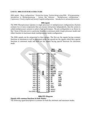
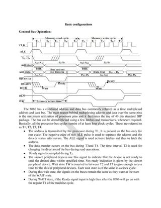
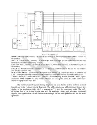
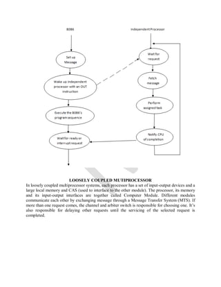
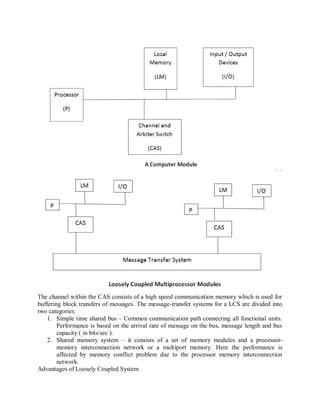
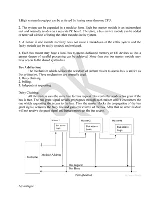
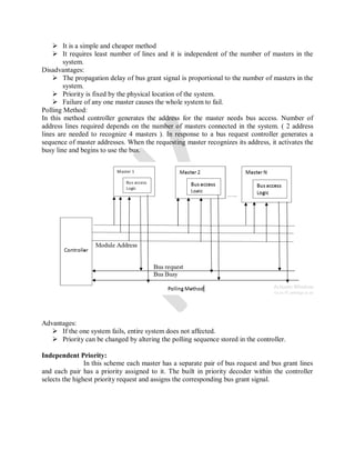
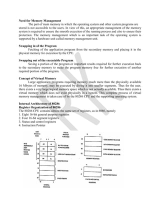
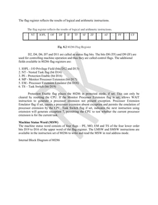
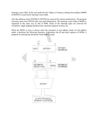
SlideShare a Scribd company logo
UNIT II - 8086 SYSTEM BUS STRUCTURE
8086 signals – Basic configurations – System bus timing –System design using 8086 – IO programming –
Introduction to Multiprogramming – System Bus Structure – Multiprocessor configurations –
Coprocessor, Closely coupled and loosely Coupled configurations – Introduction to advanced processors.
8086 signals
The 8086 Microprocessor operates in single processor or multiprocessor configurations (System
contains two or more components that can execute instructions independently, then the system is
called multiprocessor system) to achieve high performance. The pin configuration is as shown in
fig1. Some of the pins serve a particular function in minimum mode (single processor mode) and
others function in maximum mode (multiprocessor mode) configuration.
The 8086 signals can be categorized in three groups. The first are the signals having common
functions in minimum as well as maximum mode, the second are the signals which have special
functions in minimum mode and third are the signals having special functions for maximum
mode.
8086 PIN Diagram
Signals with common functions in both Modes:
The following signal description is common for both the minimum and maximum modes.
AD0-AD15 : These line are multiplexed bidirectional address/data bus. During T1 they carry lower
order address bus. In the remaining clock cycles, they carry 16 bit data. AD0-AD7 carry lower
order byte of data. AD0-AD15 carry higher order byte of data.
A19/S6, A18/S5, A17/S4, A16/S3:
During the first part of the machine cycle these are used to output upper 4-bits of address.
During remaining part of the machine cycles these are used to output status, which indicates the
type of operation to be performed in that cycle. S3 and S4 indicates the segment register being
used and S5 gives status of interrupt flag and S6 is always zero.
S4 S3 Register
0 0 ES
0 1 SS
1 0 CS or None
1 1 DS
BHE*/S7:
It stands for BUS HIGH ENABLE. It is used to indicate the transfer of data over higher order
data bus (D8-D15) if it is low. Otherwise the transfer is made on lower order byte AD7-AD0.
BHE A0 Data Access
0 0 Word
0 1 Upper byte from odd address
1 0 Lower byte from even address
1 1 None
NMI
It is a non maskable interrupt. It is an active high and an edge triggered interrupt.
INTR
It is a level triggered interrupt signal. It is active high
CLK
The clock input provides the basic timing for processor operation. Clock frequency depends on
the version of 8086.
Processor Required Clock Signal
8086 5Mhz
8086 -2 8 Mhz
8086-1 10 Mhz
RESET
It is a system reset and an active high signal. When its high, microprocessor enters into reset
states and terminates the current activity. It must be active for atleast four clock cycles to reset
the microprocessor.
READY: This is an acknowledge signal from slower I/O devices or memory. It is an active
high signal. When high, it indicates that the device is ready to transfer data. When low, then
microprocessor is in wait state.
TEST: This input is examined by a 'WAIT' instruction. If the TEST input goes low, execution
will continue, else, the processor remains in an idle state. The input is synchronized internally
during each clock cycle on leading edge of clock.
RD (Read ) : If it is low then 8086 reads data from memory or an I/O device.
MN/MX: 8080 works in two modes namely Minimum mode and Maximum mode. If it is high, it
works in minimum mode. If it is low it works in maximum mode.
PIN description / Signals in Minimum Mode: ( 24 to 31)
INTA: This is an interrupt acknowledge signal. When microprocessor receives INTR signal,
acknowledges the interrupt by generation this signal. It is an active low signal.
ALE: This is an address latch enable signal. It indicates that valid address is available on bus
AD0-AD15.It is an active high signal and remains high during T1 state.
DEN-Data Enable: This signal indicates the availability of valid data over the address/data
lines. It is used to enable the transceivers (bidirectional buffers) to separate the data from the
multiplexed address/data signal.
DT/R: This is a Data Transmit/Receive signal. It decides the direction of data flow through the
transceiver. When it is high, data is transmitted out. When it is low, data is received in.
M/IO: This signal is issued by the microprocessor to distinguish memory access from I/O access.
When it is high, memory is accessed. When it is low, I/O devices are accessed.
WR: It is a write signal. It is used to write data in memory or output device. It is an active low
signal.
HOLD and HLDA: A high on HOLD pin indicates that another master (DMA) is requesting to
take over the system bus. On receiving HOLD signal processor outputs HLDA signal HIGH as
an acknowledgement.
PIN description or signals for Maximum Mode:
QS1 and QS0 : These pins provide the status of instruction queue.
QS0 QS1 Status
0 0 No operation
0 1 1st
byte of opcode from queue
1 0 Empty queue
1 1 Subsequent byte from queue
S0, S1, S2 : These status signals indicate the operation being done by the microprocessor. This
information is required by the Bus controller 8288. Bus controller 8288 generates all memory
and I/O control signals.
S2 S1 S0 Status
0 0 0 Interrupt acknowledge
0 0 1 I/O read
0 1 0 I/O write
0 1 1 Halt
1 0 0 Opcode fetch
1 0 1 Memory read
1 1 0 Memory write
1 1 1 Inactive-passive
LOCK: This signal indicates that other processors should not ask CPU to relinquish the system
bus. When it goes low, all interrupts are masked and HOLD request is not granted.
RQ/GT1 and RQ/GT0.: These are request/ grant pins. Other processors request the CPU through
these lines to release the system bus. After receiving the request CPU Sends acknowledge signal
on the same lines.RQ/GT0 has higher priority than RQ/GT1.
*****
Basic configurations
General Bus Operation:
The 8086 has a combined address and data bus commonly referred as a time multiplexed
address and data bus. The main reason behind multiplexing address and data over the same pins
is the maximum utilization of processor pins and it facilitates the use of 40 pin standard DIP
package. The bus can be demultiplexed using a few latches and transceivers, whenever required.
Basically, all the processor bus cycles consist of at least four clock cycles. These are referred to
as T1, T2, T3, T4.
 The address is transmitted by the processor during T1, It is present on the bus only for
one cycle. The negative edge of this ALE pulse is used to separate the address and the
data or status information. The ALE signal is used activate latches and thus to latch the
address.
 The data transfer occurs on the bus during T3and T4. The time interval T2 is used for
changing the direction of the bus during read operations.
 Ready signal is sampled during T3.
 The slower peripheral devices use this signal to indicate that the device is not ready to
send the desired data within specified time. Not ready indication is given by the slower
peripheral device. Wait state TW is inserted in between T2 and T3 to give enough access
time for the slower peripheral devices. Each wait state is of the same as a clock cycle.
 During this wait state, the signals on the buses remain the same as they were at the start
of the WAIT state.
 During WAIT state, if the Ready signal input is high then after the 8086 will go on with
the regular T4 of the machine cycle.
 If the Ready input is low at the end of a WAIT state, then 8086 insert another WAIT state
until the Ready input is made high again.
 In maximum mode, the status lines S0, S1 and S2 are used to indicate the type of
operation.
 Status bits S3 to S7 are multiplexed with higher order address bits and the BHE signal.
Address is valid during T1 while status bits S3 to S7 are valid during T2 through T4.
System design using 8086
Minimum Mode 8086 System
In a minimum mode 8086 system, the microprocessor 8086 is operated in minimum mode by
strapping its MN/MX* pin to logic1. In this mode, all the control signals are given out by the
microprocessor chip itself. There is a single microprocessor in the minimum mode system. The
remaining components in the system are latches, transceivers, clock generator, memory and I/O
devices.
The figure shows the typical minimum mode 8086 system. Interacting of memory and
I/O devices are shown with the basic minimum mode 8086 configuration. Odd and even memory
banks are needed to interface with 8086. This is implemented using two EPROM and two
RAMs. Data lines D15-D8 are connected to odd bank of EPROM and RAM, and data lines D7-D0
are connected to even bank of EPROM and RAM. Address lines are connected to EPROM and
RAM. RD* signal is connected to the output enable (OE*) signals of EPROMs and RAMs. WR*
signal is connected to WR* signal of RAMs. Two separate decoders are used to generate chip
select signals for memory and I/O devices. These chip select signals are logically ORed with
either BHE* or A0 to generate final chip select signals. For generating final chip select signal for
odd bank decoder outputs are logically ORed with BHE* signal and for even bank decoder
outputs are logically ORed with A0 signal.
The 16-bit I/O interface RD* and WR* signals are connected to the RD* and WR*
signals of I/O devics. Data lines D15-D0 are connected to the data lines of I/O device. The chip
select signal for I/O device is generated using separate decoder whose output is enabled, when
M/IO* signal is low.
Bus Timing for Minimum Mode- Read operation
Read cycle timing diagram for minimum mode
 Figure shows the read cycle timing diagram. The read cycle begins in T1 with the
assertion of the address latch enable (ALE) signal and also M/IO* signal.
 During the negative going edge of this signal, the valid address is latched on the local
bus. The BHE* and A0 signals address low, high or both bytes. From Tl to T4, the
M/IO* signal indicates a memory or I/O operation.
 At T2 the address is removed from the local bus and is sent to the output. The bus is then
tristated. The read (RD*) control signal is also activated in T2 .
 The read (RD) signal causes the addressed device to enable its data bus drivers. After
RD* goes low, the valid data is available on the data bus.
 The addressed device will drive the READY line high, when the processor returns the
read signal to high level, the addressed device will again tristate its bus drivers.
Bus Timing for Minimum Mode- Write operation
Write cycle timing diagram for minimum mode
 Figure shows the write cycle timing diagram. The write cycle begins in T1 with the
assertion of the address latch enable (ALE) signal and also M/IO* signal.
 In T2 after sending the address in Tl the processor sends the data to be written to the
addressed location.
 The data remains on the bus until middle of T4 state. The WR* becomes active at the
beginning of T2
 The BHE* and A0 signals are used to select the proper byte or bytes of memory or I/O
word to be read or written. The M/IO*, RD* and WR* signals indicate the types of data
transfer as specified in table.
HOLD Response System
The figure shows the HOLD and HLDA signal timings in minimum mode system. The HOLD
pin is sampled at leading edge of each clock pulse. If it is sampled by the 8086 before T4 of the
previous cycle or during T1 of the current cycle, the 8086 activates HLDA in the next clock
cycle. It relinquishes the control of all buses and theand it is handed over to the requesting
master. The control of the bus is not regained by the 8086 until the requesting master does not
inactivate the HOLD pin. After that 8086 regains the control of buses and inactivate the HLDA
signal.
Maximum mode 8086 system
In the maximum mode, the 8086 is operated by strapping the MN/MX* pin to ground. In this
mode, the processor derives the status signals S2*, S1* and S0*. In this mode, additional
circuitry is required to translate the control signals. Th e additional circuitry is required to
converts the status signal into the I/0 and memory transfer signals.
The bus controller chip has input lines S2*, S1* and S0* and CLK. The basic functions
of the bus controller chip IC8288, is to derive control signals like RD* and WR* (for memory
and I/O devices), DEN*, DT/R*, ALE, etc. using the information made available by the
processor on the status lines. These inputs to 8288 are driven by the CPU. It derives the outputs
ALE, DEN*, DT/R*, MWTC*, AMWC*, IORC*, IOWC* and AIOWC*.
MRDC*: Memory read command – it instructs the memory to put the contents of the address location on
the data bus.
MWTC*: Memory Write Command – It instructs the memory accepts the data on the data bus and load
the data into the addressed memory location.
IORC*: I/0 Read Command – it instructs an I/O device to put the data contained in the addressed port on
the data bus.
IOWC*- I/O Write Command – It instructs an I/O device to accept the data on the data bus and load the
data into the addressed port.
MCE/PDEN*: Master Cascade Enable/ Peripheral Data Enable – It controls the mode of operation of
8259 ( Interrupt controller). It selects cascade operation of interrupt controller and I/O bus transceiver.
AIOWC*/AMWC*: Advance I/O Write Command/Advance Memory Write Command – These signals
are similar IOWC and MWTC. They will be activated one clock pulse earlier. Its useful for the slow
interfaces to prepare the input data.
The maximum mode system timing diagrams are also divided in two portions as read
(input) and write (output) timing diagrams. The address/data and address/status timings are
similar to the minimum mode. ALE is asserted in T1, just like minimum mode. The only
difference lies in the status signals used and the available control and advanced command
signals. The figures show the maximum mode timings for the read operation and for the write
operation.
Memory Read cycle
Memory Write Cycle
Multiprocessor Systems
Multiprocessor Systems refer to the use of multiple processors that execute instructions
simultaneously and communicate.
Maximum mode of 8086 is designed to implement 3 basic multiprocessor configurations:
1. Coprocessor (8087)
2. Closely coupled (dedicated I/O processor: 8089)
3. Loosely coupled (Multi bus)
Coprocessor configurations
The numeric processor 8087 is coprocessor which has been specially designed to work
under the control of the processor 8086 and to support additional numeric processing
capabilities.
FEATURES:
 It can operate on data of the integer, decimal and real types with length ranging from 2 to
10 bytes.
 Its instruction includes some useful functions like square root, exponential and tangent.
 It is high performance numeric data processor. It can multiply two 64-bit real numbers.
Pin Diagram of 8087
8087 PIN Diagram
The address/data, status ready, reset, clock and ground pins of the NDP ae similar to the
8086 pins. The other pins are as follows:
BUSY*: Busy signal from the 8087 is connected to the TEST* input of the 8086. If the 8086
needs the results of some computation, then the 8087 helps using this pin.
RQ*/GT0* : This request / grant signal from the 8087 is usually connected to the request/ grant
pin of the 8086.
INT: The 8087 can interrupt the 8086 through this pin.
S2 *- S0*:
S2* S1* S0* Status
0 X X Unused
1 0 0 Unused
1 0 1 Read memory
1 1 0 Write memory
1 1 1 Passive
QS0-QS1: These signals give the information about the queue status.
QS1 QS0 Operation
0 1 No operation
0 1 First byte of opcode from queue
1 0 Queue empty
1 1 Subsequent bytes from the queue
Interconnection of 8086 and 8087
 MN/MX* pin of the 8086 is grounded, so the 8086 is operating in its maximum mode.
 8086 sends signal on the status pins and queue status lines.
 Bus controller 8288 decodes these status signals to produce the control signals.
 The address lines A16-A9 is connected directly from 8086 to 8087.
 The 8087 receives the same clock and reset signals.
 The bus request/grant signal from 8087 is connected to the request/grant of 8086.
 The BUSY* signal from 8087 is connected to the TEST* input of 8086.
Instructions of 8087 are inserted in the 8086 programs as needed. 8086 fetches instruction bytes
from memory and puts them in its internal queue, and 8087 also reads these instruction bytes and
puts them in its internal queue.
8087 decodes each instruction from its queue and if it finds that it is an 8086 instruction, then the
8087 treats the instructions as NOP. Similarly, 8086 decodes each instruction from its queue and
if it finds that it is an 8087 instruction, then the 8086 treats the instructions as NOP. The
instructions are differentiated by code 11011. The 8087instruction code has 11011 as the most
significant bits of their code byte.
Interaction between 8086 and 8087
An instruction to be executed by 8087 is indicated by and ESC instruction. The 8087
monitors the S2* to S0 * and AD0- AD15 of 8086. The 8087 tracks status of QSO to QS1, if it is
00, 8087 does nothing. If it is 01, five MSB bits with 11011. If there is match 8087 will perform
the indicated operation. Otherwise the byte is ignored and deleted from the queue. If an error
occurs during an ESC instruction, 8087 sends an interrupt request.
8087 Architecture
Instruction Queue: it maintain a 6 byte instruction queue and tracks an execution sequence of the
host. If the current instruction is an ESC instruction, the 8087 decodes the external opcode to
perform the specified operation.
Data Register:
It has 8 data registers. Each register is 80- bit and it is accessed as a stack. A “ push “ and “pop”
operation loads and retrieve the data from stack. The top stack element is pointed by ST bits (
11,12,13 bits of the status register)
Status Register:
The status register is 16-bit register. If indicates the overall state of 8087.
B-Busy bit indicates that coprocessor is busy executing a task. Busy can be tested by
examining the status or by using the FWAIT instruction.
C3-C0 Condition code bits indicates conditions about the coprocessor.
TOP- Top of the stack (ST) bit indicates the current register address as the top of the stack.
ES-Error summary bit is set if any unmasked error bit (PE, UE, OE, ZE, DE, or IE) is set. In the
8087 the error summary is also caused a coprocessor interrupt.
PE- Precision error indicates that the result or operand executes selected precision.
UE-Under flow error indicates the result is too large to be represent with the current precision
selected by the control word.
OE-Over flow error indicates a result that is too large to be represented. If this error is masked,
the coprocessor generates infinity for an overflow error.
ZE-A Zero error indicates the divisor was zero while the dividend is a non-infinity or non-zero
number.
DE- Denormalized error indicates at least one of the operand is denormalized.
IE-Invalid error indicates a stack overflow or underflow. This flag indicates error such as those
produced by taking the square root of a negative number.
Control Register:
It is used to mask the error types individually.
 IC Infinity control
 RC Rounding control
 PC Precision control
 PM Precision control
 UM Underflow mask
 OM Overflow mask
 ZM Division by zero mask
 DM Denormalized operand mask
 IM Invalid operand mask
Stacks in 8087:
8087 has 3-bit stack pointer which holds the number of the register which is the current top- of
stack. When it is initialized, the 3-bit stack pointer in the 8087 is loaded with 000 that indicates
register 0 is a top of stack. When you decrement by one, then register 7 is the top of stack (111).
The register which is top of stack is referred as ST(0), and the register next to it is referred as
ST(1).
8087 Data types:
The 8087 recognizes three real data types:
 Short real
 Long real
 Temporary real

INSTRUCTION SET
The 8087 instruction mnemonics begins with the letter F which stands for Floating point and
distinguishes from 8086.
Types
 Data transfer instructions.
 Arithmetic instructions.
 Compare instructions.
 Transcendental instructions
Data transfer instructions:
1) Real Transfers
FLD Source - Decrements the stack pointer by one and copies a real number from a stack
element or memory location to the new ST.
Example:
FLD ST(2) – Copies ST (2) to ST.
FST Destination – C opies ST to a specified stack pointer or to a specified memory location.
Example:
FST ST(3) – Copy ST to ST(3)
FSTP destination – Copies ST to a specified stack element or memory location and increments
the stack pointer by one to point to the next element on the stack.
FXCH destination – Exchange the contents of ST with the contents of a specified stack element.
If destination is not specified then ST(1) is used.
Example:
FXCH ST(4) – Swap ST and ST(4).
2) Integer Transfer
FILD source – Convert integer number from memory to temporary-real format and load the
converted number on stack.
FIST destination – Convert number From ST to integer form and copies to memory.
FISTP destination – Similar to FIST but increment one after copy.
Arithmetic Instructions:
Addition
FADD destination, source – Add the real number in source and destination. Source can be stack
elemnt or memory location and the destination should be stack.
Example:
FADD ST(2), ST – Add ST to ST(2) and the result in ST(2)
Subtraction
FSUB destination, Source – Subtracts the real number at the specified source from the real
number at the specified destination and stores the result in the specified destination.
Example:
FSUB ST(3) , ST – Subtract ST from ST(3) and store the result in ST(3).
Multipliation
FMUL destination, source – Multiply real number from source by real number from specified
destination and store the result in specified location.
Example:
FMUL ST(2), ST - Multiply ST(2) and ST and result in ST(2).
Division
FDIV destination, source – Divide destination real number by source real and stores the result in
destination.
Example:
FDIV ST(2),ST- Divide ST by ST(2) and stores the result in ST.
COMPARE INSTRUCTIONS
Compare the contents of ST with contents of specified or default source The source may
be another stack element or real number in memory.
Examples:
FCOM source – Compare ST with real number in another stack element or memory.
FCOM ST(4) – Compare ST with ST(4).
TRANSCENDENTAL INSTRUCTIONS
FPTAN - Compute the values for a ration of Y/X for an angle in ST. The angle must be
expressed in radians.
F2XM1 – Compute the function Y=2x
– 1 for an X value in ST. Result will be stored in ST by
replacing X value.
CONSTANT INSTRUCTIONS
Load Constant Instruction – These instructions are used to push the indicated constant value
onto the stack.
FLDZ - Load +0.0
FLDI - Load+1.0
FLDPI - Load π
FLDL2T - Load log210
FLDL2E - Load log2e
FLDLG2 - Load log102
Closely Coupled System using 8086
In CCS the processors or supporting processors share clock generators, bus control logic,
entire memory and I/O system. These systems communicate through a shard main memory.
The figure shows the simplest form of closely coupled configuration. In this c8086 (CPU)
is the master and the supporting proessor is the slave. The CPU provides bus control logic. The
bus request signal from the supporting processor is connected to the CPU.
In a closely coupled system no special instruction such as WAIT or Esc is used. The
communication between processor and independent processor is done through memory space.
The host wake up independent processor by sending command to one of its port by setting
message in host memory. The independent processor access the memory to execute the task in
parallel with the host. The completion of work is indicated by interrupt request or status bit of
independent processor to the host processor.
LOOSELY COUPLED MUTIPROCESSOR
In loosely coupled multiprocessor systems, each processor has a set of input-output devices and a
large local memory and CAS (used to interface to the other module). The processor, its memory
and its input-output interfaces are together called Computer Module. Different modules
communicate each other by exchanging message through a Message Transfer System (MTS). If
more than one request comes, the channel and arbiter switch is responsible for choosing one. It’s
also responsible for delaying other requests until the servicing of the selected request is
completed.
The channel within the CAS consists of a high speed communication memory which is used for
buffering block transfers of messages. The message-transfer systems for a LCS are divided into
two categories:
1. Simple time shared bus – Common communication path connecting all functional units.
Performance is based on the arrival rate of message on the bus, message length and bus
capacity ( in bits/sec ).
2. Shared memory system – it consists of a set of memory modules and a processor-
memory interconnection network or a multiport memory. Here the performance is
affected by memory conflict problem due to the processor memory interconnection
network.
Advantages of Loosely Coupled System
1.High system throughput can be achieved by having more than one CPU.
2. The system can be expanded in a modular form. Each bus master module is an independent
unit and normally resides on a separate PC board. Therefore, a bus master module can be added
or removed without affecting the other modules in the system.
3. A failure in one module normally does not cause a breakdown of the entire system and the
faulty module can be easily detected and replaced.
4. Each bus master may have a local bus to access dedicated memory or I/O devices so that a
greater degree of parallel processing can be achieved. More than one bus master module may
have access to the shared system bus
Bus Arbitration:
The mechanism which decided the selection of current master to access bus is known as
Bus arbitration. Three mechanisms are normally used:
1. Daisy chaining.
2. Polling.
3. Independent requesting
Daisy Chaining:
All the masters uses the same line for bus request. Bus controller sends a bus grant if the
bus is free. The bus grant signal serially propagates through each master until it encounters the
one which requesting the access to the bus. Then the master blocks the propagation of the bus
grant signal, activates the busy line and gains the control of the bus. After that no other module
will not receive the grant signal and hence cannot get the bus access.
Advantages:
 It is a simple and cheaper method
 It requires least number of lines and it is independent of the number of masters in the
system.
Disadvantages:
 The propagation delay of bus grant signal is proportional to the number of masters in the
system.
 Priority is fixed by the physical location of the system.
 Failure of any one master causes the whole system to fail.
Polling Method:
In this method controller generates the address for the master needs bus access. Number of
address lines required depends on the number of masters connected in the system. ( 2 address
lines are needed to recognize 4 masters ). In response to a bus request controller generates a
sequence of master addresses. When the requesting master recognizes its address, it activates the
busy line and begins to use the bus.
Advantages:
 If the one system fails, entire system does not affected.
 Priority can be changed by altering the polling sequence stored in the controller.
Independent Priority:
In this scheme each master has a separate pair of bus request and bus grant lines
and each pair has a priority assigned to it. The built in priority decoder within the controller
selects the highest priority request and assigns the corresponding bus grant signal.
Advantages:
Bus arbitration is fast and it is independent of the number of masters in the system.
Disadvantages:
It requires more bus request and grant signals.
Introduction to Advanced Processors
The 80286 is the first member of the family of advanced microprocessors with memory
management and protection abilities. The 80286 CPU, with its 24-bit address bus is able to
address 16 Mbytes of physical memory. Various versions of 80286 are available that runs on
12.5 MHz , 10 MHz and 8 MHz clock frequencies. 80286 is upwardly compatible with 8086 in
terms of instruction set.
80286 has two operating modes namely real address mode and virtual address mode. In
real address mode, the 80286 can address upto 1Mb of physical memory address like 8086. In
virtual address mode, it can address up to 16 Mb of physical memory address space and 1 Gb of
virtual memory address space. The instruction set of 80286 includes the instructions of 8086 and
80186.
80286 has some extra instructions to support operating system and memory management.
In real address mode, the 80286 is object code compatible with 8086. In protected virtual address
mode, it is source code compatible with 8086. The performance of 80286 is five times faster than
the standard 8086.
Need for Memory Management
The part of main memory in which the operating system and other system programs are
stored is not accessible to the users. In view of this, an appropriate management of the memory
system is required to ensure the smooth execution of the running process and also to ensure their
protection. The memory management which is an important task of the operating system is
supported by a hardware unit called memory management unit.
Swapping in of the Program
Fetching of the application program from the secondary memory and placing it in the
physical memory for execution by the CPU.
Swapping out of the executable Program
Saving a portion of the program or important results required for further execution back
to the secondary memory to make the program memory free for further execution of another
required portion of the program.
Concept of Virtual Memory
Large application programs requiring memory much more than the physically available
16 Mbytes of memory, may be executed by diving it into smaller segments. Thus for the user,
there exists a very large logical memory space which is not actually available. Thus there exists a
virtual memory which does not exist physically in a system. This complete process of virtual
memory management is taken care of by the 80286 CPU and the supporting operating system.
Internal Architecture of 80286
Register Organization of 80286
The 80286 CPU contains almost the same set of registers, as in 8086, namely
1. Eight 16-bit general purpose registers
2. Four 16-bit segment registers
3. Status and control registers
4. Instruction Pointer
The flag register reflects the results of logical and arithmetic instructions.
D2, D4, D6, D7 and D11 are called as status flag bits. The bits D8 (TF) and D9 (IF) are
used for controlling machine operation and thus they are called control flags. The additional
fields available in 80286 flag registers are:
1. IOPL - I/O Privilege Field (bits D12 and D13)
2. NT - Nested Task flag (bit D14)
3. PE - Protection Enable (bit D16)
4. MP - Monitor Processor Extension (bit D17)
5. EM - Processor Extension Emulator (bit D18)
6. TS – Task Switch (bit D19)
Protection Enable flag places the 80286 in protected mode, if set. This can only be
cleared by resetting the CPU. If the Monitor Processor Extension flag is set, allows WAIT
instruction to generate a processor extension not present exception. Processor Extension
Emulator flag if set, causes a processor extension absent exception and permits the emulation of
processor extension by the CPU. Task Switch flag if set, indicates the next instruction using
extension will generate exception 7, permitting the CPU to test whether the current processor
extension is for the current task.
Machine Status Word (MSW)
The machine status word consists of four flags – PE, MO, EM and TS of the four lower order
bits D19 to D16 of the upper word of the flag register. The LMSW and SMSW instructions are
available in the instruction set of 80286 to write and read the MSW in real address mode.
Internal Block Diagram of 80286
The CPU contain four functional blocks
1. Address Unit (AU)
2. Bus Init (BU)
3. Instruction Unit (IU)
4. Execution Unit (EU)
The address unit is responsible for calculating the physical address of instructions and
data that the CPU wants to access. Also the address lines derived by this unit may be used to
address different peripherals. The physical address computed by the address unit is handed over
to the bus unit (BU) of the CPU. Major function of the bus unit is to fetch instruction bytes from
the memory. Instructions are fetched in advance and stored in a queue to enable faster execution
of the instructions. The bus unit also contains a bus control module that controls the prefetcher
module. These prefetched instructions are arranged in a 6-byte instructions queue. The 6-byte
prefetch queue forwards the instructions arranged in it to the instruction unit (IU). The
instruction unit accepts instructions from the prefetch queue and an instruction decoder decodes
them one by one. The decoded instructions are latched onto a decoded instruction queue. The
output of the decoding circuit drives a control circuit in the execution unit, which is responsible
for executing the instructions received from decoded instruction queue.
The decoded instruction queue sends the data part of the instruction over the data bus.
The EU contains the register bank used for storing the data as scratch pad, or used as special
purpose registers. The ALU, the heart of the EU, carries out all the arithmetic and logical
operations and sends the results over the data bus or back to the register bank.
Interrupts of 80286
The Interrupts of 80286 may be divided into three categories,
1. External or hardware interrupts
2. INT instruction or software interrupts
3. Interrupts generated internally by exceptions
While executing an instruction, the CPU may sometimes be confronted with a special
situation because of which further execution is not permitted. While trying to execute a divide by
zero instruction, the CPU detects a major error and stops further execution. In this case, we say
that an exception has been generated. In other words, an instruction exception is an unusual
situation encountered during execution of an instruction that stops further execution. The return
address from an exception, in most of the cases, points to the instruction that caused the
exception.
As in the case of 8086, the interrupt vector table of 80286 requires 1Kbytes of space for
storing 256, four-byte pointers to point to the corresponding 256 interrupt service routines (lSR).
Each pointer contains a 16-bit offset followed by a 16-bit segment selector to point to a particular
ISR. The calculation of vector pointer address in the interrupt vector table from the (8-bit) INT
type is exactly similar to 8086. Like 8086, the 80286 supports the software interrupts of type 0
(INT 00) to type FFH (INT FFH).
Maskable Interrupt INTR : This is a maskable interrupt input pin of which the INT type is to
be provided by an external circuit like an interrupt controller. The other functional details of this
interrupt pin are exactly similar to the INTR input of 8086.
Non-Maskable Interrupt NMI : It has higher priority than the INTR interrupt. Whenever this
interrupt is received, a vector value of 02 is supplied internally to calculate the pointer to the
interrupt vector table. Once the CPU responds to a NMI request, it does not serve any other
interrupt request (including NMI). Further it does not serve the processor extension
(coprocessor) segment overrun interrupt, till either it executes IRET or it is reset. To start with,
this clears the IF flag which is set again with the execution of IRET, i.e. return from interrupt.
Single Step Interrupt
As in 8086, this is an internal interrupt that comes into action, if trap flag (TF) of 80286 is set.
The CPU stops the execution after each instruction cycle so that the register contents (including
flag register), the program status word and memory, etc. may be examined at the end of each
instruction execution. This interrupt is useful for troubleshooting the software. An interrupt
vector type 01 is reserved for this interrupt.
Interrupt Priorities:
If more than one interrupt signals occur simultaneously, they are processed according to
their priorities as shown below :
Order Interrupt
1 Interrupt exception
2 Single step
3 NMI
4 Processor extension segment overrun
5 INTR
6 INT instruction
FUNCTION Interrupt Number
Divide error exception 0
Single step interrupt 1
NMI interrupt 2
Breakpoint interrupt 3
INTO detected overflow exception 4
BOUND range exceeded exception 5
Invalid opcode exception 6
Processor extension not available exception 7
Intel reserved, do not use 8-15
Processor extension error interrupt 16
Intel reserved, do not use 17-31
User defined 32-255
Signal Description of 80286
CLK: This is the system clock input pin. The clock frequency applied at this pin is divided by
two internally and is used for deriving fundamental timings for basic operations of the circuit.
The clock is generated using 8284 clock generator.
D15-D0 : These are sixteen bidirectional data bus lines.
A23-A0 : These are the physical address output lines used to address memory or I/O devices.
The address lines A23 - A16 are zero during I/O transfers.
BHE : This output signal, as in 8086, indicates that there is a transfer on the higher byte of the
data bus (D15 – D8) .
S1 , S0 : These are the active-low status output signals which indicate initiation of a bus cycle
and with M/IO and COD/INTA, they define the type of the bus cycle.
M/ IO : This output line differentiates memory operations from I/O operations. If this signal is it
“0” indicates that an I/O cycle or INTA cycle is in process and if it is “1” it indicates that a
memory or a HALT cycle is in progress.
COD/ INTA : This output signal, in combination with M/ IO signal and S1 , S0 distinguishes
different memory, I/O and INTA cycles.
LOCK : This active-low output pin is used to prevent the other masters from gaining the control
of the bus for the current and the following bus cycles. This pin is activated by a "LOCK"
instruction prefix, or automatically by hardware during XCHG, interrupt acknowledge or
descriptor table access
READY This active-low input pin is used to insert wait states in a bus cycle, for interfacing low
speed peripherals. This signal is neglected during HLDA cycle.
HOLD and HLDA This pair of pins is used by external bus masters to request for the control of
the system bus (HOLD) and to check whether the main processor has granted the control
(HLDA) or not, in the same way as it was in 8086.
INTR : Through this active high input, an external device requests 80286 to suspend the current
instruction execution and serve the interrupt request. Its function is exactly similar to that of
INTR pin of 8086.
NMI : The Non-Maskable Interrupt request is an active-high, edge-triggered input that is
equivalent to an INTR signal of type 2. No acknowledge cycles are needed to be carried out.
PEREG and PEACK (Processor Extension Request and Acknowledgement) Processor extension
refers to coprocessor (80287 in case of 80286 CPU). This pair of pins extends the memory
management and protection capabilities of 80286 to the processor extension 80287. The PEREQ
input requests the 80286 to perform a data operand transfer for a processor extension. The
PEACK active-low output indicates to the processor extension that the requested operand is
being transferred.
BUSY and ERROR : Processor extension BUSY and ERROR active-low input signals indicate
the operating conditions of a processor extension to 80286. The BUSY goes low, indicating
80286 to suspend the execution and wait until the BUSY become inactive. In this duration, the
processor extension is busy with its allotted job. Once the job is completed the processor
extension drives the BUSY input high indicating 80286 to continue with the program execution.
An active ERROR signal causes the 80286 to perform the processor extension interrupt while
executing the WAIT and ESC instructions. The active ERROR signal indicates to 80286 that the
processor extension has committed a mistake and hence it is reactivating the processor extension
interrupt.
CAP : A 0.047 μf, 12V capacitor must be connected between this input pin and ground to filter
the output of the internal substrate bias generator. For correct operation of 80286 the capacitor
must be charged to its operating voltage. Till this capacitor charges to its full capacity, the 80286
may be kept stuck to reset to avoid any spurious activity.
Vss : This pin is a system ground pin of 80286.
Vcc : This pin is used to apply +5V power supply voltage to the internal circuit of 80286.
RESET The active-high RESET input clears the internal logic of 80286, and reinitializes
RESET The active-high reset input pulse width should be at least 16 clock cycles. The 80286
requires at least 38 clock cycles after the trailing edge of the RESET input signal, before it makes
the first opcode fetch cycle.
Real Address Mode
• Act as a fast 8086
• Instruction set is upwardly compatible
• It address only 1 M byte of physical memory using A0-A19.
• In real addressing mode of operation of 80286, it just acts as a fast 8086. The
instruction set is upward compatible with that of 8086.
The 80286 addresses only 1Mbytes of physical memory using A0- A19. The lines A20-A23 are
not used by the internal circuit of 80286 in this mode. In real address mode, while addressing the
physical memory, the 80286 uses BHE along with A0- A19. The 20-bit physical address is again
formed in the same way as that in 8086. The contents of segment registers are used as segment
base addresses.
The other registers, depending upon the addressing mode, contain the offset addresses. Because
of extra pipelining and other circuit level improvements, in real address mode also, the 80286
operates at a much faster rate than 8086, although functionally they work in an identical fashion.
As in 8086, the physical memory is organized in terms of segments of 64Kbyte maximum size.
An exception is generated, if the segment size limit is exceeded by the instruction or the data.
The overlapping of physical memory segments is allowed to minimize the memory requirements
for a task. The 80286 reserves two fixed areas of physical memory for system initialization and
interrupt vector table. In the real mode the first 1Kbyte of memory starting from address 0000H
to 003FFH is reserved for interrupt vector table.
Also the addresses from FFFF0H to FFFFFH are reserved for system initialization. The program
execution starts from FFFFH after reset and initialization. The interrupt vector table of 80286 is
organized in the same way as that of 8086. Some of the interrupt types are reserved for
exceptions, single-stepping and processor extension segment overrun, etc.
When the 80286 is reset, it always starts the execution in real address mode. In real address
mode, it performs the following functions: it initializes the IP and other registers of 80286, it
prepares for entering the protected virtual address mode.
PROTECTED VIRTUAL ADDRESS MODE (PVAM)
80286 is the first processor to support the concepts of virtual memory and memory
management. The virtual memory does not exist physically it still appears to be available within
the system. The concept of VM is implemented using Physical memory that the CPU can directly
access and secondary memory that is used as storage for data and program, which are stored in
secondary memory initially.
The Segment of the program or data required for actual execution at that instant, is
fetched from the secondary memory into physical memory. After the execution of this fetched
segment, the next segment required for further execution is again fetched from the secondary
memory, while the results of the executed segment are stored back into the secondary memory
for further references. This continues till the complete program is executed.
During the execution the partial results of the previously executed portions are again
fetched into the physical memory, if required for further execution. The procedure of fetching the
chosen program segments or data from the secondary storage into physical memory is called
swapping. The procedure of storing back the partial results or data back on the secondary storage
is called unswapping. The virtual memory is allotted per task.
The 80286 is able to address 1 G byte (230 bytes) of virtual memory per task. The
complete virtual memory is mapped on to the 16Mbyte physical memory. If a program larger
than 16Mbyte is stored on the hard disk and is to be executed , if it is fetched in terms of data or
program segments of less than 16Mbyte in size into the program memory by swapping
sequentially as per sequence of execution.
Whenever the portion of a program is required for execution by the CPU, it is fetched
from the secondary memory and placed in the physical memory is called swapping in of the
program. A portion of the program or important partial results required for further execution,
may be saved back on secondary storage to make the PM free for further execution of another
required portion of the program is called swapping out of the executable program .
80286 uses the 16-bit content of a segment register as a selector to address a descriptor
stored in the physical memory. The descriptor is a block of contiguous memory locations
containing information of a segment, like segment base address, segment limit, segment type,
privilege level, segment availability in physical memory, descriptor type and segment use
another task.
unit 4 mc.pdf

More Related Content

Similar to unit 4 mc.pdf

Application of 8086 and 8085 Microprocessor in Robots.pptx
Application of 8086 and 8085 Microprocessor in Robots.pptxApplication of 8086 and 8085 Microprocessor in Robots.pptx
Application of 8086 and 8085 Microprocessor in Robots.pptxssuser631ea0
 
8086 Programing.ppt
8086 Programing.ppt8086 Programing.ppt
8086 Programing.pptDrRRAMAN
 
8086 Microprocessor by Nitish Nagar
8086 Microprocessor by Nitish Nagar8086 Microprocessor by Nitish Nagar
8086 Microprocessor by Nitish NagarNitish Nagar
 
8086 modes
8086 modes8086 modes
8086 modesPDFSHARE
 
PIN Specification of 8086 Microprocessor
PIN Specification of 8086 MicroprocessorPIN Specification of 8086 Microprocessor
PIN Specification of 8086 MicroprocessorNikhil Kumar
 
MICROPROCESSOR AND INTERFACING
MICROPROCESSOR AND INTERFACING MICROPROCESSOR AND INTERFACING
MICROPROCESSOR AND INTERFACING Radhika Talaviya
 
Pin Description and Register Organization of 8086 Microprocessor
Pin Description and Register Organization of 8086 MicroprocessorPin Description and Register Organization of 8086 Microprocessor
Pin Description and Register Organization of 8086 MicroprocessorMuthusamy Arumugam
 
Minimum mode and Maximum mode Configuration in 8086
Minimum mode and Maximum mode Configuration in 8086Minimum mode and Maximum mode Configuration in 8086
Minimum mode and Maximum mode Configuration in 8086Jismy .K.Jose
 
8086-microprocessor
8086-microprocessor8086-microprocessor
8086-microprocessorjhcid
 
Minimum Modes and Maximum Modes of 8086 Microprocessor
Minimum Modes and Maximum Modes of 8086 MicroprocessorMinimum Modes and Maximum Modes of 8086 Microprocessor
Minimum Modes and Maximum Modes of 8086 MicroprocessorNikhil Kumar
 
8086 – CPU –Pin Diagram.pptx
8086 – CPU –Pin Diagram.pptx8086 – CPU –Pin Diagram.pptx
8086 – CPU –Pin Diagram.pptx5G8Rajendra
 
Pin configuration of 8085
Pin configuration of 8085Pin configuration of 8085
Pin configuration of 808582338476
 
Intel 8086 internal architecture & pin diagram
Intel 8086 internal architecture & pin diagramIntel 8086 internal architecture & pin diagram
Intel 8086 internal architecture & pin diagramkrunal47
 
29. 8086 microprocessor pin diagram
29. 8086 microprocessor pin diagram29. 8086 microprocessor pin diagram
29. 8086 microprocessor pin diagramsandip das
 
An alarm system is to have 4 different devices, each with its sensor..pdf
An alarm system is to have 4 different devices, each with its sensor..pdfAn alarm system is to have 4 different devices, each with its sensor..pdf
An alarm system is to have 4 different devices, each with its sensor..pdfleventhalbrad49439
 

Similar to unit 4 mc.pdf (20)

Application of 8086 and 8085 Microprocessor in Robots.pptx
Application of 8086 and 8085 Microprocessor in Robots.pptxApplication of 8086 and 8085 Microprocessor in Robots.pptx
Application of 8086 and 8085 Microprocessor in Robots.pptx
 
8086 Programing.ppt
8086 Programing.ppt8086 Programing.ppt
8086 Programing.ppt
 
8086 Microprocessor by Nitish Nagar
8086 Microprocessor by Nitish Nagar8086 Microprocessor by Nitish Nagar
8086 Microprocessor by Nitish Nagar
 
8086 modes
8086 modes8086 modes
8086 modes
 
Mpmc
MpmcMpmc
Mpmc
 
MINIMUM MODE INTERFACE
MINIMUM MODE INTERFACEMINIMUM MODE INTERFACE
MINIMUM MODE INTERFACE
 
PIN Specification of 8086 Microprocessor
PIN Specification of 8086 MicroprocessorPIN Specification of 8086 Microprocessor
PIN Specification of 8086 Microprocessor
 
MICROPROCESSOR AND INTERFACING
MICROPROCESSOR AND INTERFACING MICROPROCESSOR AND INTERFACING
MICROPROCESSOR AND INTERFACING
 
Pin Description and Register Organization of 8086 Microprocessor
Pin Description and Register Organization of 8086 MicroprocessorPin Description and Register Organization of 8086 Microprocessor
Pin Description and Register Organization of 8086 Microprocessor
 
Minimum mode and Maximum mode Configuration in 8086
Minimum mode and Maximum mode Configuration in 8086Minimum mode and Maximum mode Configuration in 8086
Minimum mode and Maximum mode Configuration in 8086
 
8086-microprocessor
8086-microprocessor8086-microprocessor
8086-microprocessor
 
Minimum Modes and Maximum Modes of 8086 Microprocessor
Minimum Modes and Maximum Modes of 8086 MicroprocessorMinimum Modes and Maximum Modes of 8086 Microprocessor
Minimum Modes and Maximum Modes of 8086 Microprocessor
 
8086 datasheet
8086 datasheet8086 datasheet
8086 datasheet
 
8086 datasheet
8086 datasheet8086 datasheet
8086 datasheet
 
8086 – CPU –Pin Diagram.pptx
8086 – CPU –Pin Diagram.pptx8086 – CPU –Pin Diagram.pptx
8086 – CPU –Pin Diagram.pptx
 
Pin configuration of 8085
Pin configuration of 8085Pin configuration of 8085
Pin configuration of 8085
 
Intel 8086 internal architecture & pin diagram
Intel 8086 internal architecture & pin diagramIntel 8086 internal architecture & pin diagram
Intel 8086 internal architecture & pin diagram
 
8086 complete guide
8086 complete guide 8086 complete guide
8086 complete guide
 
29. 8086 microprocessor pin diagram
29. 8086 microprocessor pin diagram29. 8086 microprocessor pin diagram
29. 8086 microprocessor pin diagram
 
An alarm system is to have 4 different devices, each with its sensor..pdf
An alarm system is to have 4 different devices, each with its sensor..pdfAn alarm system is to have 4 different devices, each with its sensor..pdf
An alarm system is to have 4 different devices, each with its sensor..pdf
 

Recently uploaded

Furniture showroom management system project.pdf
Furniture showroom management system project.pdfFurniture showroom management system project.pdf
Furniture showroom management system project.pdfKamal Acharya
 
Introduction to Machine Learning Unit-4 Notes for II-II Mechanical Engineering
Introduction to Machine Learning Unit-4 Notes for II-II Mechanical EngineeringIntroduction to Machine Learning Unit-4 Notes for II-II Mechanical Engineering
Introduction to Machine Learning Unit-4 Notes for II-II Mechanical EngineeringC Sai Kiran
 
Event Management System Vb Net Project Report.pdf
Event Management System Vb Net  Project Report.pdfEvent Management System Vb Net  Project Report.pdf
Event Management System Vb Net Project Report.pdfKamal Acharya
 
Top 13 Famous Civil Engineering Scientist
Top 13 Famous Civil Engineering ScientistTop 13 Famous Civil Engineering Scientist
Top 13 Famous Civil Engineering Scientistgettygaming1
 
ASME IX(9) 2007 Full Version .pdf
ASME IX(9)  2007 Full Version       .pdfASME IX(9)  2007 Full Version       .pdf
ASME IX(9) 2007 Full Version .pdfAhmedHussein950959
 
KIT-601 Lecture Notes-UNIT-3.pdf Mining Data Stream
KIT-601 Lecture Notes-UNIT-3.pdf Mining Data StreamKIT-601 Lecture Notes-UNIT-3.pdf Mining Data Stream
KIT-601 Lecture Notes-UNIT-3.pdf Mining Data StreamDr. Radhey Shyam
 
Scaling in conventional MOSFET for constant electric field and constant voltage
Scaling in conventional MOSFET for constant electric field and constant voltageScaling in conventional MOSFET for constant electric field and constant voltage
Scaling in conventional MOSFET for constant electric field and constant voltageRCC Institute of Information Technology
 
KIT-601 Lecture Notes-UNIT-5.pdf Frame Works and Visualization
KIT-601 Lecture Notes-UNIT-5.pdf Frame Works and VisualizationKIT-601 Lecture Notes-UNIT-5.pdf Frame Works and Visualization
KIT-601 Lecture Notes-UNIT-5.pdf Frame Works and VisualizationDr. Radhey Shyam
 
ONLINE VEHICLE RENTAL SYSTEM PROJECT REPORT.pdf
ONLINE VEHICLE RENTAL SYSTEM PROJECT REPORT.pdfONLINE VEHICLE RENTAL SYSTEM PROJECT REPORT.pdf
ONLINE VEHICLE RENTAL SYSTEM PROJECT REPORT.pdfKamal Acharya
 
School management system project report.pdf
School management system project report.pdfSchool management system project report.pdf
School management system project report.pdfKamal Acharya
 
KIT-601 Lecture Notes-UNIT-4.pdf Frequent Itemsets and Clustering
KIT-601 Lecture Notes-UNIT-4.pdf Frequent Itemsets and ClusteringKIT-601 Lecture Notes-UNIT-4.pdf Frequent Itemsets and Clustering
KIT-601 Lecture Notes-UNIT-4.pdf Frequent Itemsets and ClusteringDr. Radhey Shyam
 
shape functions of 1D and 2 D rectangular elements.pptx
shape functions of 1D and 2 D rectangular elements.pptxshape functions of 1D and 2 D rectangular elements.pptx
shape functions of 1D and 2 D rectangular elements.pptxVishalDeshpande27
 
retail automation billing system ppt.pptx
retail automation billing system ppt.pptxretail automation billing system ppt.pptx
retail automation billing system ppt.pptxfaamieahmd
 
Explosives Industry manufacturing process.pdf
Explosives Industry manufacturing process.pdfExplosives Industry manufacturing process.pdf
Explosives Industry manufacturing process.pdf884710SadaqatAli
 
Construction method of steel structure space frame .pptx
Construction method of steel structure space frame .pptxConstruction method of steel structure space frame .pptx
Construction method of steel structure space frame .pptxwendy cai
 
Introduction to Machine Learning Unit-5 Notes for II-II Mechanical Engineering
Introduction to Machine Learning Unit-5 Notes for II-II Mechanical EngineeringIntroduction to Machine Learning Unit-5 Notes for II-II Mechanical Engineering
Introduction to Machine Learning Unit-5 Notes for II-II Mechanical EngineeringC Sai Kiran
 
A case study of cinema management system project report..pdf
A case study of cinema management system project report..pdfA case study of cinema management system project report..pdf
A case study of cinema management system project report..pdfKamal Acharya
 
Natalia Rutkowska - BIM School Course in Kraków
Natalia Rutkowska - BIM School Course in KrakówNatalia Rutkowska - BIM School Course in Kraków
Natalia Rutkowska - BIM School Course in Krakówbim.edu.pl
 
Courier management system project report.pdf
Courier management system project report.pdfCourier management system project report.pdf
Courier management system project report.pdfKamal Acharya
 
NO1 Pandit Black Magic Removal in Uk kala jadu Specialist kala jadu for Love ...
NO1 Pandit Black Magic Removal in Uk kala jadu Specialist kala jadu for Love ...NO1 Pandit Black Magic Removal in Uk kala jadu Specialist kala jadu for Love ...
NO1 Pandit Black Magic Removal in Uk kala jadu Specialist kala jadu for Love ...Amil baba
 

Recently uploaded (20)

Furniture showroom management system project.pdf
Furniture showroom management system project.pdfFurniture showroom management system project.pdf
Furniture showroom management system project.pdf
 
Introduction to Machine Learning Unit-4 Notes for II-II Mechanical Engineering
Introduction to Machine Learning Unit-4 Notes for II-II Mechanical EngineeringIntroduction to Machine Learning Unit-4 Notes for II-II Mechanical Engineering
Introduction to Machine Learning Unit-4 Notes for II-II Mechanical Engineering
 
Event Management System Vb Net Project Report.pdf
Event Management System Vb Net  Project Report.pdfEvent Management System Vb Net  Project Report.pdf
Event Management System Vb Net Project Report.pdf
 
Top 13 Famous Civil Engineering Scientist
Top 13 Famous Civil Engineering ScientistTop 13 Famous Civil Engineering Scientist
Top 13 Famous Civil Engineering Scientist
 
ASME IX(9) 2007 Full Version .pdf
ASME IX(9)  2007 Full Version       .pdfASME IX(9)  2007 Full Version       .pdf
ASME IX(9) 2007 Full Version .pdf
 
KIT-601 Lecture Notes-UNIT-3.pdf Mining Data Stream
KIT-601 Lecture Notes-UNIT-3.pdf Mining Data StreamKIT-601 Lecture Notes-UNIT-3.pdf Mining Data Stream
KIT-601 Lecture Notes-UNIT-3.pdf Mining Data Stream
 
Scaling in conventional MOSFET for constant electric field and constant voltage
Scaling in conventional MOSFET for constant electric field and constant voltageScaling in conventional MOSFET for constant electric field and constant voltage
Scaling in conventional MOSFET for constant electric field and constant voltage
 
KIT-601 Lecture Notes-UNIT-5.pdf Frame Works and Visualization
KIT-601 Lecture Notes-UNIT-5.pdf Frame Works and VisualizationKIT-601 Lecture Notes-UNIT-5.pdf Frame Works and Visualization
KIT-601 Lecture Notes-UNIT-5.pdf Frame Works and Visualization
 
ONLINE VEHICLE RENTAL SYSTEM PROJECT REPORT.pdf
ONLINE VEHICLE RENTAL SYSTEM PROJECT REPORT.pdfONLINE VEHICLE RENTAL SYSTEM PROJECT REPORT.pdf
ONLINE VEHICLE RENTAL SYSTEM PROJECT REPORT.pdf
 
School management system project report.pdf
School management system project report.pdfSchool management system project report.pdf
School management system project report.pdf
 
KIT-601 Lecture Notes-UNIT-4.pdf Frequent Itemsets and Clustering
KIT-601 Lecture Notes-UNIT-4.pdf Frequent Itemsets and ClusteringKIT-601 Lecture Notes-UNIT-4.pdf Frequent Itemsets and Clustering
KIT-601 Lecture Notes-UNIT-4.pdf Frequent Itemsets and Clustering
 
shape functions of 1D and 2 D rectangular elements.pptx
shape functions of 1D and 2 D rectangular elements.pptxshape functions of 1D and 2 D rectangular elements.pptx
shape functions of 1D and 2 D rectangular elements.pptx
 
retail automation billing system ppt.pptx
retail automation billing system ppt.pptxretail automation billing system ppt.pptx
retail automation billing system ppt.pptx
 
Explosives Industry manufacturing process.pdf
Explosives Industry manufacturing process.pdfExplosives Industry manufacturing process.pdf
Explosives Industry manufacturing process.pdf
 
Construction method of steel structure space frame .pptx
Construction method of steel structure space frame .pptxConstruction method of steel structure space frame .pptx
Construction method of steel structure space frame .pptx
 
Introduction to Machine Learning Unit-5 Notes for II-II Mechanical Engineering
Introduction to Machine Learning Unit-5 Notes for II-II Mechanical EngineeringIntroduction to Machine Learning Unit-5 Notes for II-II Mechanical Engineering
Introduction to Machine Learning Unit-5 Notes for II-II Mechanical Engineering
 
A case study of cinema management system project report..pdf
A case study of cinema management system project report..pdfA case study of cinema management system project report..pdf
A case study of cinema management system project report..pdf
 
Natalia Rutkowska - BIM School Course in Kraków
Natalia Rutkowska - BIM School Course in KrakówNatalia Rutkowska - BIM School Course in Kraków
Natalia Rutkowska - BIM School Course in Kraków
 
Courier management system project report.pdf
Courier management system project report.pdfCourier management system project report.pdf
Courier management system project report.pdf
 
NO1 Pandit Black Magic Removal in Uk kala jadu Specialist kala jadu for Love ...
NO1 Pandit Black Magic Removal in Uk kala jadu Specialist kala jadu for Love ...NO1 Pandit Black Magic Removal in Uk kala jadu Specialist kala jadu for Love ...
NO1 Pandit Black Magic Removal in Uk kala jadu Specialist kala jadu for Love ...
 

unit 4 mc.pdf

  • 1. UNIT II - 8086 SYSTEM BUS STRUCTURE 8086 signals – Basic configurations – System bus timing –System design using 8086 – IO programming – Introduction to Multiprogramming – System Bus Structure – Multiprocessor configurations – Coprocessor, Closely coupled and loosely Coupled configurations – Introduction to advanced processors. 8086 signals The 8086 Microprocessor operates in single processor or multiprocessor configurations (System contains two or more components that can execute instructions independently, then the system is called multiprocessor system) to achieve high performance. The pin configuration is as shown in fig1. Some of the pins serve a particular function in minimum mode (single processor mode) and others function in maximum mode (multiprocessor mode) configuration. The 8086 signals can be categorized in three groups. The first are the signals having common functions in minimum as well as maximum mode, the second are the signals which have special functions in minimum mode and third are the signals having special functions for maximum mode. 8086 PIN Diagram Signals with common functions in both Modes: The following signal description is common for both the minimum and maximum modes.
  • 2. AD0-AD15 : These line are multiplexed bidirectional address/data bus. During T1 they carry lower order address bus. In the remaining clock cycles, they carry 16 bit data. AD0-AD7 carry lower order byte of data. AD0-AD15 carry higher order byte of data. A19/S6, A18/S5, A17/S4, A16/S3: During the first part of the machine cycle these are used to output upper 4-bits of address. During remaining part of the machine cycles these are used to output status, which indicates the type of operation to be performed in that cycle. S3 and S4 indicates the segment register being used and S5 gives status of interrupt flag and S6 is always zero. S4 S3 Register 0 0 ES 0 1 SS 1 0 CS or None 1 1 DS BHE*/S7: It stands for BUS HIGH ENABLE. It is used to indicate the transfer of data over higher order data bus (D8-D15) if it is low. Otherwise the transfer is made on lower order byte AD7-AD0. BHE A0 Data Access 0 0 Word 0 1 Upper byte from odd address 1 0 Lower byte from even address 1 1 None NMI It is a non maskable interrupt. It is an active high and an edge triggered interrupt. INTR It is a level triggered interrupt signal. It is active high CLK The clock input provides the basic timing for processor operation. Clock frequency depends on the version of 8086. Processor Required Clock Signal 8086 5Mhz 8086 -2 8 Mhz 8086-1 10 Mhz RESET It is a system reset and an active high signal. When its high, microprocessor enters into reset states and terminates the current activity. It must be active for atleast four clock cycles to reset the microprocessor.
  • 3. READY: This is an acknowledge signal from slower I/O devices or memory. It is an active high signal. When high, it indicates that the device is ready to transfer data. When low, then microprocessor is in wait state. TEST: This input is examined by a 'WAIT' instruction. If the TEST input goes low, execution will continue, else, the processor remains in an idle state. The input is synchronized internally during each clock cycle on leading edge of clock. RD (Read ) : If it is low then 8086 reads data from memory or an I/O device. MN/MX: 8080 works in two modes namely Minimum mode and Maximum mode. If it is high, it works in minimum mode. If it is low it works in maximum mode. PIN description / Signals in Minimum Mode: ( 24 to 31) INTA: This is an interrupt acknowledge signal. When microprocessor receives INTR signal, acknowledges the interrupt by generation this signal. It is an active low signal. ALE: This is an address latch enable signal. It indicates that valid address is available on bus AD0-AD15.It is an active high signal and remains high during T1 state. DEN-Data Enable: This signal indicates the availability of valid data over the address/data lines. It is used to enable the transceivers (bidirectional buffers) to separate the data from the multiplexed address/data signal. DT/R: This is a Data Transmit/Receive signal. It decides the direction of data flow through the transceiver. When it is high, data is transmitted out. When it is low, data is received in. M/IO: This signal is issued by the microprocessor to distinguish memory access from I/O access. When it is high, memory is accessed. When it is low, I/O devices are accessed. WR: It is a write signal. It is used to write data in memory or output device. It is an active low signal. HOLD and HLDA: A high on HOLD pin indicates that another master (DMA) is requesting to take over the system bus. On receiving HOLD signal processor outputs HLDA signal HIGH as an acknowledgement. PIN description or signals for Maximum Mode: QS1 and QS0 : These pins provide the status of instruction queue. QS0 QS1 Status 0 0 No operation
  • 4. 0 1 1st byte of opcode from queue 1 0 Empty queue 1 1 Subsequent byte from queue S0, S1, S2 : These status signals indicate the operation being done by the microprocessor. This information is required by the Bus controller 8288. Bus controller 8288 generates all memory and I/O control signals. S2 S1 S0 Status 0 0 0 Interrupt acknowledge 0 0 1 I/O read 0 1 0 I/O write 0 1 1 Halt 1 0 0 Opcode fetch 1 0 1 Memory read 1 1 0 Memory write 1 1 1 Inactive-passive LOCK: This signal indicates that other processors should not ask CPU to relinquish the system bus. When it goes low, all interrupts are masked and HOLD request is not granted. RQ/GT1 and RQ/GT0.: These are request/ grant pins. Other processors request the CPU through these lines to release the system bus. After receiving the request CPU Sends acknowledge signal on the same lines.RQ/GT0 has higher priority than RQ/GT1. *****
  • 5. Basic configurations General Bus Operation: The 8086 has a combined address and data bus commonly referred as a time multiplexed address and data bus. The main reason behind multiplexing address and data over the same pins is the maximum utilization of processor pins and it facilitates the use of 40 pin standard DIP package. The bus can be demultiplexed using a few latches and transceivers, whenever required. Basically, all the processor bus cycles consist of at least four clock cycles. These are referred to as T1, T2, T3, T4.  The address is transmitted by the processor during T1, It is present on the bus only for one cycle. The negative edge of this ALE pulse is used to separate the address and the data or status information. The ALE signal is used activate latches and thus to latch the address.  The data transfer occurs on the bus during T3and T4. The time interval T2 is used for changing the direction of the bus during read operations.  Ready signal is sampled during T3.  The slower peripheral devices use this signal to indicate that the device is not ready to send the desired data within specified time. Not ready indication is given by the slower peripheral device. Wait state TW is inserted in between T2 and T3 to give enough access time for the slower peripheral devices. Each wait state is of the same as a clock cycle.  During this wait state, the signals on the buses remain the same as they were at the start of the WAIT state.  During WAIT state, if the Ready signal input is high then after the 8086 will go on with the regular T4 of the machine cycle.
  • 6.  If the Ready input is low at the end of a WAIT state, then 8086 insert another WAIT state until the Ready input is made high again.  In maximum mode, the status lines S0, S1 and S2 are used to indicate the type of operation.  Status bits S3 to S7 are multiplexed with higher order address bits and the BHE signal. Address is valid during T1 while status bits S3 to S7 are valid during T2 through T4. System design using 8086 Minimum Mode 8086 System In a minimum mode 8086 system, the microprocessor 8086 is operated in minimum mode by strapping its MN/MX* pin to logic1. In this mode, all the control signals are given out by the microprocessor chip itself. There is a single microprocessor in the minimum mode system. The remaining components in the system are latches, transceivers, clock generator, memory and I/O devices. The figure shows the typical minimum mode 8086 system. Interacting of memory and I/O devices are shown with the basic minimum mode 8086 configuration. Odd and even memory banks are needed to interface with 8086. This is implemented using two EPROM and two RAMs. Data lines D15-D8 are connected to odd bank of EPROM and RAM, and data lines D7-D0 are connected to even bank of EPROM and RAM. Address lines are connected to EPROM and RAM. RD* signal is connected to the output enable (OE*) signals of EPROMs and RAMs. WR* signal is connected to WR* signal of RAMs. Two separate decoders are used to generate chip select signals for memory and I/O devices. These chip select signals are logically ORed with either BHE* or A0 to generate final chip select signals. For generating final chip select signal for odd bank decoder outputs are logically ORed with BHE* signal and for even bank decoder outputs are logically ORed with A0 signal. The 16-bit I/O interface RD* and WR* signals are connected to the RD* and WR* signals of I/O devics. Data lines D15-D0 are connected to the data lines of I/O device. The chip select signal for I/O device is generated using separate decoder whose output is enabled, when M/IO* signal is low.
  • 7. Bus Timing for Minimum Mode- Read operation Read cycle timing diagram for minimum mode  Figure shows the read cycle timing diagram. The read cycle begins in T1 with the assertion of the address latch enable (ALE) signal and also M/IO* signal.
  • 8.  During the negative going edge of this signal, the valid address is latched on the local bus. The BHE* and A0 signals address low, high or both bytes. From Tl to T4, the M/IO* signal indicates a memory or I/O operation.  At T2 the address is removed from the local bus and is sent to the output. The bus is then tristated. The read (RD*) control signal is also activated in T2 .  The read (RD) signal causes the addressed device to enable its data bus drivers. After RD* goes low, the valid data is available on the data bus.  The addressed device will drive the READY line high, when the processor returns the read signal to high level, the addressed device will again tristate its bus drivers. Bus Timing for Minimum Mode- Write operation Write cycle timing diagram for minimum mode  Figure shows the write cycle timing diagram. The write cycle begins in T1 with the assertion of the address latch enable (ALE) signal and also M/IO* signal.  In T2 after sending the address in Tl the processor sends the data to be written to the addressed location.  The data remains on the bus until middle of T4 state. The WR* becomes active at the beginning of T2  The BHE* and A0 signals are used to select the proper byte or bytes of memory or I/O word to be read or written. The M/IO*, RD* and WR* signals indicate the types of data transfer as specified in table.
  • 9. HOLD Response System The figure shows the HOLD and HLDA signal timings in minimum mode system. The HOLD pin is sampled at leading edge of each clock pulse. If it is sampled by the 8086 before T4 of the previous cycle or during T1 of the current cycle, the 8086 activates HLDA in the next clock cycle. It relinquishes the control of all buses and theand it is handed over to the requesting master. The control of the bus is not regained by the 8086 until the requesting master does not inactivate the HOLD pin. After that 8086 regains the control of buses and inactivate the HLDA signal. Maximum mode 8086 system In the maximum mode, the 8086 is operated by strapping the MN/MX* pin to ground. In this mode, the processor derives the status signals S2*, S1* and S0*. In this mode, additional circuitry is required to translate the control signals. Th e additional circuitry is required to converts the status signal into the I/0 and memory transfer signals. The bus controller chip has input lines S2*, S1* and S0* and CLK. The basic functions of the bus controller chip IC8288, is to derive control signals like RD* and WR* (for memory and I/O devices), DEN*, DT/R*, ALE, etc. using the information made available by the processor on the status lines. These inputs to 8288 are driven by the CPU. It derives the outputs ALE, DEN*, DT/R*, MWTC*, AMWC*, IORC*, IOWC* and AIOWC*.
  • 10. MRDC*: Memory read command – it instructs the memory to put the contents of the address location on the data bus. MWTC*: Memory Write Command – It instructs the memory accepts the data on the data bus and load the data into the addressed memory location. IORC*: I/0 Read Command – it instructs an I/O device to put the data contained in the addressed port on the data bus. IOWC*- I/O Write Command – It instructs an I/O device to accept the data on the data bus and load the data into the addressed port. MCE/PDEN*: Master Cascade Enable/ Peripheral Data Enable – It controls the mode of operation of 8259 ( Interrupt controller). It selects cascade operation of interrupt controller and I/O bus transceiver. AIOWC*/AMWC*: Advance I/O Write Command/Advance Memory Write Command – These signals are similar IOWC and MWTC. They will be activated one clock pulse earlier. Its useful for the slow interfaces to prepare the input data. The maximum mode system timing diagrams are also divided in two portions as read (input) and write (output) timing diagrams. The address/data and address/status timings are similar to the minimum mode. ALE is asserted in T1, just like minimum mode. The only difference lies in the status signals used and the available control and advanced command signals. The figures show the maximum mode timings for the read operation and for the write operation.
  • 12. Multiprocessor Systems Multiprocessor Systems refer to the use of multiple processors that execute instructions simultaneously and communicate. Maximum mode of 8086 is designed to implement 3 basic multiprocessor configurations: 1. Coprocessor (8087) 2. Closely coupled (dedicated I/O processor: 8089) 3. Loosely coupled (Multi bus) Coprocessor configurations The numeric processor 8087 is coprocessor which has been specially designed to work under the control of the processor 8086 and to support additional numeric processing capabilities. FEATURES:  It can operate on data of the integer, decimal and real types with length ranging from 2 to 10 bytes.  Its instruction includes some useful functions like square root, exponential and tangent.  It is high performance numeric data processor. It can multiply two 64-bit real numbers. Pin Diagram of 8087
  • 13. 8087 PIN Diagram The address/data, status ready, reset, clock and ground pins of the NDP ae similar to the 8086 pins. The other pins are as follows: BUSY*: Busy signal from the 8087 is connected to the TEST* input of the 8086. If the 8086 needs the results of some computation, then the 8087 helps using this pin. RQ*/GT0* : This request / grant signal from the 8087 is usually connected to the request/ grant pin of the 8086. INT: The 8087 can interrupt the 8086 through this pin. S2 *- S0*: S2* S1* S0* Status 0 X X Unused 1 0 0 Unused 1 0 1 Read memory 1 1 0 Write memory 1 1 1 Passive QS0-QS1: These signals give the information about the queue status. QS1 QS0 Operation 0 1 No operation
  • 14. 0 1 First byte of opcode from queue 1 0 Queue empty 1 1 Subsequent bytes from the queue Interconnection of 8086 and 8087  MN/MX* pin of the 8086 is grounded, so the 8086 is operating in its maximum mode.  8086 sends signal on the status pins and queue status lines.  Bus controller 8288 decodes these status signals to produce the control signals.  The address lines A16-A9 is connected directly from 8086 to 8087.  The 8087 receives the same clock and reset signals.  The bus request/grant signal from 8087 is connected to the request/grant of 8086.  The BUSY* signal from 8087 is connected to the TEST* input of 8086. Instructions of 8087 are inserted in the 8086 programs as needed. 8086 fetches instruction bytes from memory and puts them in its internal queue, and 8087 also reads these instruction bytes and puts them in its internal queue.
  • 15. 8087 decodes each instruction from its queue and if it finds that it is an 8086 instruction, then the 8087 treats the instructions as NOP. Similarly, 8086 decodes each instruction from its queue and if it finds that it is an 8087 instruction, then the 8086 treats the instructions as NOP. The instructions are differentiated by code 11011. The 8087instruction code has 11011 as the most significant bits of their code byte. Interaction between 8086 and 8087 An instruction to be executed by 8087 is indicated by and ESC instruction. The 8087 monitors the S2* to S0 * and AD0- AD15 of 8086. The 8087 tracks status of QSO to QS1, if it is 00, 8087 does nothing. If it is 01, five MSB bits with 11011. If there is match 8087 will perform the indicated operation. Otherwise the byte is ignored and deleted from the queue. If an error occurs during an ESC instruction, 8087 sends an interrupt request.
  • 16. 8087 Architecture Instruction Queue: it maintain a 6 byte instruction queue and tracks an execution sequence of the host. If the current instruction is an ESC instruction, the 8087 decodes the external opcode to perform the specified operation. Data Register: It has 8 data registers. Each register is 80- bit and it is accessed as a stack. A “ push “ and “pop” operation loads and retrieve the data from stack. The top stack element is pointed by ST bits ( 11,12,13 bits of the status register) Status Register: The status register is 16-bit register. If indicates the overall state of 8087.
  • 17. B-Busy bit indicates that coprocessor is busy executing a task. Busy can be tested by examining the status or by using the FWAIT instruction. C3-C0 Condition code bits indicates conditions about the coprocessor. TOP- Top of the stack (ST) bit indicates the current register address as the top of the stack. ES-Error summary bit is set if any unmasked error bit (PE, UE, OE, ZE, DE, or IE) is set. In the 8087 the error summary is also caused a coprocessor interrupt. PE- Precision error indicates that the result or operand executes selected precision. UE-Under flow error indicates the result is too large to be represent with the current precision selected by the control word. OE-Over flow error indicates a result that is too large to be represented. If this error is masked, the coprocessor generates infinity for an overflow error. ZE-A Zero error indicates the divisor was zero while the dividend is a non-infinity or non-zero number. DE- Denormalized error indicates at least one of the operand is denormalized. IE-Invalid error indicates a stack overflow or underflow. This flag indicates error such as those produced by taking the square root of a negative number. Control Register: It is used to mask the error types individually.  IC Infinity control  RC Rounding control  PC Precision control
  • 18.  PM Precision control  UM Underflow mask  OM Overflow mask  ZM Division by zero mask  DM Denormalized operand mask  IM Invalid operand mask Stacks in 8087: 8087 has 3-bit stack pointer which holds the number of the register which is the current top- of stack. When it is initialized, the 3-bit stack pointer in the 8087 is loaded with 000 that indicates register 0 is a top of stack. When you decrement by one, then register 7 is the top of stack (111). The register which is top of stack is referred as ST(0), and the register next to it is referred as ST(1). 8087 Data types: The 8087 recognizes three real data types:  Short real  Long real  Temporary real  INSTRUCTION SET The 8087 instruction mnemonics begins with the letter F which stands for Floating point and distinguishes from 8086. Types  Data transfer instructions.  Arithmetic instructions.  Compare instructions.  Transcendental instructions Data transfer instructions: 1) Real Transfers FLD Source - Decrements the stack pointer by one and copies a real number from a stack element or memory location to the new ST. Example: FLD ST(2) – Copies ST (2) to ST. FST Destination – C opies ST to a specified stack pointer or to a specified memory location. Example: FST ST(3) – Copy ST to ST(3) FSTP destination – Copies ST to a specified stack element or memory location and increments the stack pointer by one to point to the next element on the stack. FXCH destination – Exchange the contents of ST with the contents of a specified stack element. If destination is not specified then ST(1) is used. Example: FXCH ST(4) – Swap ST and ST(4). 2) Integer Transfer
  • 19. FILD source – Convert integer number from memory to temporary-real format and load the converted number on stack. FIST destination – Convert number From ST to integer form and copies to memory. FISTP destination – Similar to FIST but increment one after copy. Arithmetic Instructions: Addition FADD destination, source – Add the real number in source and destination. Source can be stack elemnt or memory location and the destination should be stack. Example: FADD ST(2), ST – Add ST to ST(2) and the result in ST(2) Subtraction FSUB destination, Source – Subtracts the real number at the specified source from the real number at the specified destination and stores the result in the specified destination. Example: FSUB ST(3) , ST – Subtract ST from ST(3) and store the result in ST(3). Multipliation FMUL destination, source – Multiply real number from source by real number from specified destination and store the result in specified location. Example: FMUL ST(2), ST - Multiply ST(2) and ST and result in ST(2). Division FDIV destination, source – Divide destination real number by source real and stores the result in destination. Example: FDIV ST(2),ST- Divide ST by ST(2) and stores the result in ST. COMPARE INSTRUCTIONS Compare the contents of ST with contents of specified or default source The source may be another stack element or real number in memory. Examples: FCOM source – Compare ST with real number in another stack element or memory. FCOM ST(4) – Compare ST with ST(4). TRANSCENDENTAL INSTRUCTIONS FPTAN - Compute the values for a ration of Y/X for an angle in ST. The angle must be expressed in radians. F2XM1 – Compute the function Y=2x – 1 for an X value in ST. Result will be stored in ST by replacing X value. CONSTANT INSTRUCTIONS
  • 20. Load Constant Instruction – These instructions are used to push the indicated constant value onto the stack. FLDZ - Load +0.0 FLDI - Load+1.0 FLDPI - Load π FLDL2T - Load log210 FLDL2E - Load log2e FLDLG2 - Load log102 Closely Coupled System using 8086 In CCS the processors or supporting processors share clock generators, bus control logic, entire memory and I/O system. These systems communicate through a shard main memory. The figure shows the simplest form of closely coupled configuration. In this c8086 (CPU) is the master and the supporting proessor is the slave. The CPU provides bus control logic. The bus request signal from the supporting processor is connected to the CPU. In a closely coupled system no special instruction such as WAIT or Esc is used. The communication between processor and independent processor is done through memory space. The host wake up independent processor by sending command to one of its port by setting message in host memory. The independent processor access the memory to execute the task in parallel with the host. The completion of work is indicated by interrupt request or status bit of independent processor to the host processor.
  • 21. LOOSELY COUPLED MUTIPROCESSOR In loosely coupled multiprocessor systems, each processor has a set of input-output devices and a large local memory and CAS (used to interface to the other module). The processor, its memory and its input-output interfaces are together called Computer Module. Different modules communicate each other by exchanging message through a Message Transfer System (MTS). If more than one request comes, the channel and arbiter switch is responsible for choosing one. It’s also responsible for delaying other requests until the servicing of the selected request is completed.
  • 22. The channel within the CAS consists of a high speed communication memory which is used for buffering block transfers of messages. The message-transfer systems for a LCS are divided into two categories: 1. Simple time shared bus – Common communication path connecting all functional units. Performance is based on the arrival rate of message on the bus, message length and bus capacity ( in bits/sec ). 2. Shared memory system – it consists of a set of memory modules and a processor- memory interconnection network or a multiport memory. Here the performance is affected by memory conflict problem due to the processor memory interconnection network. Advantages of Loosely Coupled System
  • 23. 1.High system throughput can be achieved by having more than one CPU. 2. The system can be expanded in a modular form. Each bus master module is an independent unit and normally resides on a separate PC board. Therefore, a bus master module can be added or removed without affecting the other modules in the system. 3. A failure in one module normally does not cause a breakdown of the entire system and the faulty module can be easily detected and replaced. 4. Each bus master may have a local bus to access dedicated memory or I/O devices so that a greater degree of parallel processing can be achieved. More than one bus master module may have access to the shared system bus Bus Arbitration: The mechanism which decided the selection of current master to access bus is known as Bus arbitration. Three mechanisms are normally used: 1. Daisy chaining. 2. Polling. 3. Independent requesting Daisy Chaining: All the masters uses the same line for bus request. Bus controller sends a bus grant if the bus is free. The bus grant signal serially propagates through each master until it encounters the one which requesting the access to the bus. Then the master blocks the propagation of the bus grant signal, activates the busy line and gains the control of the bus. After that no other module will not receive the grant signal and hence cannot get the bus access. Advantages:
  • 24.  It is a simple and cheaper method  It requires least number of lines and it is independent of the number of masters in the system. Disadvantages:  The propagation delay of bus grant signal is proportional to the number of masters in the system.  Priority is fixed by the physical location of the system.  Failure of any one master causes the whole system to fail. Polling Method: In this method controller generates the address for the master needs bus access. Number of address lines required depends on the number of masters connected in the system. ( 2 address lines are needed to recognize 4 masters ). In response to a bus request controller generates a sequence of master addresses. When the requesting master recognizes its address, it activates the busy line and begins to use the bus. Advantages:  If the one system fails, entire system does not affected.  Priority can be changed by altering the polling sequence stored in the controller. Independent Priority: In this scheme each master has a separate pair of bus request and bus grant lines and each pair has a priority assigned to it. The built in priority decoder within the controller selects the highest priority request and assigns the corresponding bus grant signal.
  • 25. Advantages: Bus arbitration is fast and it is independent of the number of masters in the system. Disadvantages: It requires more bus request and grant signals. Introduction to Advanced Processors The 80286 is the first member of the family of advanced microprocessors with memory management and protection abilities. The 80286 CPU, with its 24-bit address bus is able to address 16 Mbytes of physical memory. Various versions of 80286 are available that runs on 12.5 MHz , 10 MHz and 8 MHz clock frequencies. 80286 is upwardly compatible with 8086 in terms of instruction set. 80286 has two operating modes namely real address mode and virtual address mode. In real address mode, the 80286 can address upto 1Mb of physical memory address like 8086. In virtual address mode, it can address up to 16 Mb of physical memory address space and 1 Gb of virtual memory address space. The instruction set of 80286 includes the instructions of 8086 and 80186. 80286 has some extra instructions to support operating system and memory management. In real address mode, the 80286 is object code compatible with 8086. In protected virtual address mode, it is source code compatible with 8086. The performance of 80286 is five times faster than the standard 8086.
  • 26. Need for Memory Management The part of main memory in which the operating system and other system programs are stored is not accessible to the users. In view of this, an appropriate management of the memory system is required to ensure the smooth execution of the running process and also to ensure their protection. The memory management which is an important task of the operating system is supported by a hardware unit called memory management unit. Swapping in of the Program Fetching of the application program from the secondary memory and placing it in the physical memory for execution by the CPU. Swapping out of the executable Program Saving a portion of the program or important results required for further execution back to the secondary memory to make the program memory free for further execution of another required portion of the program. Concept of Virtual Memory Large application programs requiring memory much more than the physically available 16 Mbytes of memory, may be executed by diving it into smaller segments. Thus for the user, there exists a very large logical memory space which is not actually available. Thus there exists a virtual memory which does not exist physically in a system. This complete process of virtual memory management is taken care of by the 80286 CPU and the supporting operating system. Internal Architecture of 80286 Register Organization of 80286 The 80286 CPU contains almost the same set of registers, as in 8086, namely 1. Eight 16-bit general purpose registers 2. Four 16-bit segment registers 3. Status and control registers 4. Instruction Pointer
  • 27. The flag register reflects the results of logical and arithmetic instructions. D2, D4, D6, D7 and D11 are called as status flag bits. The bits D8 (TF) and D9 (IF) are used for controlling machine operation and thus they are called control flags. The additional fields available in 80286 flag registers are: 1. IOPL - I/O Privilege Field (bits D12 and D13) 2. NT - Nested Task flag (bit D14) 3. PE - Protection Enable (bit D16) 4. MP - Monitor Processor Extension (bit D17) 5. EM - Processor Extension Emulator (bit D18) 6. TS – Task Switch (bit D19) Protection Enable flag places the 80286 in protected mode, if set. This can only be cleared by resetting the CPU. If the Monitor Processor Extension flag is set, allows WAIT instruction to generate a processor extension not present exception. Processor Extension Emulator flag if set, causes a processor extension absent exception and permits the emulation of processor extension by the CPU. Task Switch flag if set, indicates the next instruction using extension will generate exception 7, permitting the CPU to test whether the current processor extension is for the current task. Machine Status Word (MSW) The machine status word consists of four flags – PE, MO, EM and TS of the four lower order bits D19 to D16 of the upper word of the flag register. The LMSW and SMSW instructions are available in the instruction set of 80286 to write and read the MSW in real address mode. Internal Block Diagram of 80286
  • 28. The CPU contain four functional blocks 1. Address Unit (AU) 2. Bus Init (BU) 3. Instruction Unit (IU) 4. Execution Unit (EU) The address unit is responsible for calculating the physical address of instructions and data that the CPU wants to access. Also the address lines derived by this unit may be used to address different peripherals. The physical address computed by the address unit is handed over to the bus unit (BU) of the CPU. Major function of the bus unit is to fetch instruction bytes from the memory. Instructions are fetched in advance and stored in a queue to enable faster execution of the instructions. The bus unit also contains a bus control module that controls the prefetcher module. These prefetched instructions are arranged in a 6-byte instructions queue. The 6-byte prefetch queue forwards the instructions arranged in it to the instruction unit (IU). The instruction unit accepts instructions from the prefetch queue and an instruction decoder decodes them one by one. The decoded instructions are latched onto a decoded instruction queue. The output of the decoding circuit drives a control circuit in the execution unit, which is responsible for executing the instructions received from decoded instruction queue. The decoded instruction queue sends the data part of the instruction over the data bus. The EU contains the register bank used for storing the data as scratch pad, or used as special purpose registers. The ALU, the heart of the EU, carries out all the arithmetic and logical operations and sends the results over the data bus or back to the register bank.
  • 29. Interrupts of 80286 The Interrupts of 80286 may be divided into three categories, 1. External or hardware interrupts 2. INT instruction or software interrupts 3. Interrupts generated internally by exceptions While executing an instruction, the CPU may sometimes be confronted with a special situation because of which further execution is not permitted. While trying to execute a divide by zero instruction, the CPU detects a major error and stops further execution. In this case, we say that an exception has been generated. In other words, an instruction exception is an unusual situation encountered during execution of an instruction that stops further execution. The return address from an exception, in most of the cases, points to the instruction that caused the exception. As in the case of 8086, the interrupt vector table of 80286 requires 1Kbytes of space for storing 256, four-byte pointers to point to the corresponding 256 interrupt service routines (lSR). Each pointer contains a 16-bit offset followed by a 16-bit segment selector to point to a particular ISR. The calculation of vector pointer address in the interrupt vector table from the (8-bit) INT type is exactly similar to 8086. Like 8086, the 80286 supports the software interrupts of type 0 (INT 00) to type FFH (INT FFH). Maskable Interrupt INTR : This is a maskable interrupt input pin of which the INT type is to be provided by an external circuit like an interrupt controller. The other functional details of this interrupt pin are exactly similar to the INTR input of 8086. Non-Maskable Interrupt NMI : It has higher priority than the INTR interrupt. Whenever this interrupt is received, a vector value of 02 is supplied internally to calculate the pointer to the interrupt vector table. Once the CPU responds to a NMI request, it does not serve any other interrupt request (including NMI). Further it does not serve the processor extension (coprocessor) segment overrun interrupt, till either it executes IRET or it is reset. To start with, this clears the IF flag which is set again with the execution of IRET, i.e. return from interrupt. Single Step Interrupt As in 8086, this is an internal interrupt that comes into action, if trap flag (TF) of 80286 is set. The CPU stops the execution after each instruction cycle so that the register contents (including flag register), the program status word and memory, etc. may be examined at the end of each instruction execution. This interrupt is useful for troubleshooting the software. An interrupt vector type 01 is reserved for this interrupt. Interrupt Priorities: If more than one interrupt signals occur simultaneously, they are processed according to their priorities as shown below : Order Interrupt 1 Interrupt exception 2 Single step 3 NMI
  • 30. 4 Processor extension segment overrun 5 INTR 6 INT instruction FUNCTION Interrupt Number Divide error exception 0 Single step interrupt 1 NMI interrupt 2 Breakpoint interrupt 3 INTO detected overflow exception 4 BOUND range exceeded exception 5 Invalid opcode exception 6 Processor extension not available exception 7 Intel reserved, do not use 8-15 Processor extension error interrupt 16 Intel reserved, do not use 17-31 User defined 32-255 Signal Description of 80286 CLK: This is the system clock input pin. The clock frequency applied at this pin is divided by two internally and is used for deriving fundamental timings for basic operations of the circuit. The clock is generated using 8284 clock generator. D15-D0 : These are sixteen bidirectional data bus lines. A23-A0 : These are the physical address output lines used to address memory or I/O devices. The address lines A23 - A16 are zero during I/O transfers. BHE : This output signal, as in 8086, indicates that there is a transfer on the higher byte of the data bus (D15 – D8) . S1 , S0 : These are the active-low status output signals which indicate initiation of a bus cycle and with M/IO and COD/INTA, they define the type of the bus cycle. M/ IO : This output line differentiates memory operations from I/O operations. If this signal is it “0” indicates that an I/O cycle or INTA cycle is in process and if it is “1” it indicates that a memory or a HALT cycle is in progress. COD/ INTA : This output signal, in combination with M/ IO signal and S1 , S0 distinguishes different memory, I/O and INTA cycles. LOCK : This active-low output pin is used to prevent the other masters from gaining the control of the bus for the current and the following bus cycles. This pin is activated by a "LOCK" instruction prefix, or automatically by hardware during XCHG, interrupt acknowledge or descriptor table access
  • 31.
  • 32. READY This active-low input pin is used to insert wait states in a bus cycle, for interfacing low speed peripherals. This signal is neglected during HLDA cycle. HOLD and HLDA This pair of pins is used by external bus masters to request for the control of the system bus (HOLD) and to check whether the main processor has granted the control (HLDA) or not, in the same way as it was in 8086. INTR : Through this active high input, an external device requests 80286 to suspend the current instruction execution and serve the interrupt request. Its function is exactly similar to that of INTR pin of 8086. NMI : The Non-Maskable Interrupt request is an active-high, edge-triggered input that is equivalent to an INTR signal of type 2. No acknowledge cycles are needed to be carried out. PEREG and PEACK (Processor Extension Request and Acknowledgement) Processor extension refers to coprocessor (80287 in case of 80286 CPU). This pair of pins extends the memory management and protection capabilities of 80286 to the processor extension 80287. The PEREQ input requests the 80286 to perform a data operand transfer for a processor extension. The PEACK active-low output indicates to the processor extension that the requested operand is being transferred. BUSY and ERROR : Processor extension BUSY and ERROR active-low input signals indicate the operating conditions of a processor extension to 80286. The BUSY goes low, indicating 80286 to suspend the execution and wait until the BUSY become inactive. In this duration, the
  • 33. processor extension is busy with its allotted job. Once the job is completed the processor extension drives the BUSY input high indicating 80286 to continue with the program execution. An active ERROR signal causes the 80286 to perform the processor extension interrupt while executing the WAIT and ESC instructions. The active ERROR signal indicates to 80286 that the processor extension has committed a mistake and hence it is reactivating the processor extension interrupt. CAP : A 0.047 μf, 12V capacitor must be connected between this input pin and ground to filter the output of the internal substrate bias generator. For correct operation of 80286 the capacitor must be charged to its operating voltage. Till this capacitor charges to its full capacity, the 80286 may be kept stuck to reset to avoid any spurious activity. Vss : This pin is a system ground pin of 80286. Vcc : This pin is used to apply +5V power supply voltage to the internal circuit of 80286. RESET The active-high RESET input clears the internal logic of 80286, and reinitializes RESET The active-high reset input pulse width should be at least 16 clock cycles. The 80286 requires at least 38 clock cycles after the trailing edge of the RESET input signal, before it makes the first opcode fetch cycle. Real Address Mode • Act as a fast 8086 • Instruction set is upwardly compatible • It address only 1 M byte of physical memory using A0-A19. • In real addressing mode of operation of 80286, it just acts as a fast 8086. The instruction set is upward compatible with that of 8086. The 80286 addresses only 1Mbytes of physical memory using A0- A19. The lines A20-A23 are not used by the internal circuit of 80286 in this mode. In real address mode, while addressing the physical memory, the 80286 uses BHE along with A0- A19. The 20-bit physical address is again formed in the same way as that in 8086. The contents of segment registers are used as segment base addresses. The other registers, depending upon the addressing mode, contain the offset addresses. Because of extra pipelining and other circuit level improvements, in real address mode also, the 80286 operates at a much faster rate than 8086, although functionally they work in an identical fashion. As in 8086, the physical memory is organized in terms of segments of 64Kbyte maximum size. An exception is generated, if the segment size limit is exceeded by the instruction or the data. The overlapping of physical memory segments is allowed to minimize the memory requirements for a task. The 80286 reserves two fixed areas of physical memory for system initialization and
  • 34. interrupt vector table. In the real mode the first 1Kbyte of memory starting from address 0000H to 003FFH is reserved for interrupt vector table. Also the addresses from FFFF0H to FFFFFH are reserved for system initialization. The program execution starts from FFFFH after reset and initialization. The interrupt vector table of 80286 is organized in the same way as that of 8086. Some of the interrupt types are reserved for exceptions, single-stepping and processor extension segment overrun, etc. When the 80286 is reset, it always starts the execution in real address mode. In real address mode, it performs the following functions: it initializes the IP and other registers of 80286, it prepares for entering the protected virtual address mode.
  • 35. PROTECTED VIRTUAL ADDRESS MODE (PVAM) 80286 is the first processor to support the concepts of virtual memory and memory management. The virtual memory does not exist physically it still appears to be available within the system. The concept of VM is implemented using Physical memory that the CPU can directly access and secondary memory that is used as storage for data and program, which are stored in secondary memory initially. The Segment of the program or data required for actual execution at that instant, is fetched from the secondary memory into physical memory. After the execution of this fetched segment, the next segment required for further execution is again fetched from the secondary memory, while the results of the executed segment are stored back into the secondary memory for further references. This continues till the complete program is executed. During the execution the partial results of the previously executed portions are again fetched into the physical memory, if required for further execution. The procedure of fetching the chosen program segments or data from the secondary storage into physical memory is called swapping. The procedure of storing back the partial results or data back on the secondary storage is called unswapping. The virtual memory is allotted per task. The 80286 is able to address 1 G byte (230 bytes) of virtual memory per task. The complete virtual memory is mapped on to the 16Mbyte physical memory. If a program larger than 16Mbyte is stored on the hard disk and is to be executed , if it is fetched in terms of data or program segments of less than 16Mbyte in size into the program memory by swapping sequentially as per sequence of execution. Whenever the portion of a program is required for execution by the CPU, it is fetched from the secondary memory and placed in the physical memory is called swapping in of the program. A portion of the program or important partial results required for further execution, may be saved back on secondary storage to make the PM free for further execution of another required portion of the program is called swapping out of the executable program . 80286 uses the 16-bit content of a segment register as a selector to address a descriptor stored in the physical memory. The descriptor is a block of contiguous memory locations containing information of a segment, like segment base address, segment limit, segment type, privilege level, segment availability in physical memory, descriptor type and segment use another task.