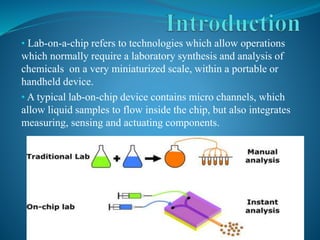
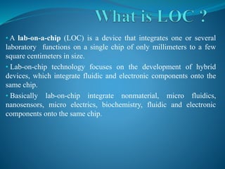
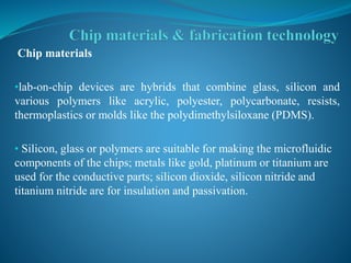
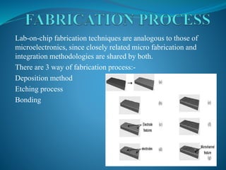
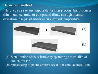
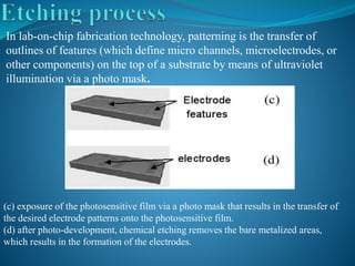
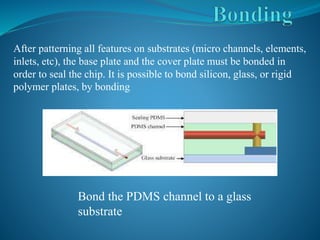
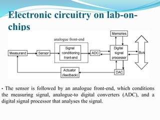
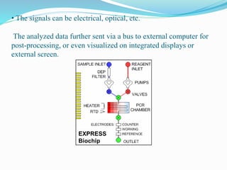
A part of nanotechnology. Nanosensors is very hot topic for research. As nanosensor has immense applications in the fields like medical, analysis, research etc. Nanosensor recude the cost and also the time require for analysis.
MEMS is a technique of combining electrical and mechanical components together on a chip. It produces a system of miniature dimensions i.e the system having thickness less than the thickness of human hair. The components are integrated on a single chip using micro fabrication technology which allows the microsystem to both sense & control the environment.
It was a review project that is typically more focused on mechanical parts and microfabrication technologies made suitable for biological applications.
The interdisciplinary nature of bio-MEMS combines material sciences, clinical sciences, medicine, surgery, electrical engineering, mechanical engineering, optical engineering, chemical engineering and biomedical engineering.
Some of its major applications include genomics, proteomics, molecular diagnostics, point-of-care diagnostics, tissue engineering and implantable microdevices. MEMS techniques were originally developed in the microelectronics industry.
MEMS are a class of miniature devices and systems fabricated by micromachining processes. MEMS devices have critical dimensions in the range of 100nm to 1000um (or 1mm).
MEMS technology is a precursor to the relatively more popular field of Nanotechnology, which refers to science, engineering and technology below 100nm down to the atomic scale.
Occasionally, MEMS devices with dimensions in the millimetre-range are referred to as meso-scale MEMS devices. as drug delivery systems improve, the components of the systems continue to decrease in size.
Currently, most drug delivery systems are based upon devices and drug carrier elements that are on a micro-scale. Many of the future and developing technologies are based on the nano-scale.
The following presentation is only for quick reference. I would advise you to read the theoretical aspects of the respective topic and then use this presentation for your last minute revision. I hope it helps you..!!
Mayur D. Chauhan
What is MEMS?
Micro electro mechanical system is a technique of combining electrical and mechanical combinations together on a chip, to produce a system of miniature dimensions.
MEMS is a integration of a number micro components on a single chip which allow the microsystem to both sense and control the environment.
The components are integrated on a single chip using micro fabrication technologies.
This webinar was hosted in partnership with Quantum Computing & Simulation Hub, by the Quantum Technologies Innovation Network https://ktn-uk.org/quantum/.
Learn of the potential of cryo-electronics in quantum computing and other disciplines.
Cryogenic electronics is of critical importance in many fields including quantum technologies, astronomy and particle physics. This event was designed to bring scientists, engineers and industry across all relevant disciplines to advance the integration of electronics at cryogenic temperatures and combine resources to solve common challenges.
With this meeting, we hope to progress towards demonstrating the relevance and market size of cryogenic electronics. We welcome foundries and industry stakeholders in considering further engagement with this technology and present a state-of-the-art picture for all relevant stakeholders.
Micro-Electro-Mechanical Systems, or MEMS, is a technology that in its most general form can be defined as miniaturized mechanical and electro-mechanical elements (i.e., devices and structures) that are made using the techniques of microfabrication. The critical physical dimensions of MEMS devices can vary from well below one micron on the lower end of the dimensional spectrum, all the way to several millimeters. Likewise, the types of MEMS devices can vary from relatively simple structures having no moving elements, to extremely complex electromechanical systems with multiple moving elements under the control of integrated microelectronics. The one main criterion of MEMS is that there are at least some elements having some sort of mechanical functionality whether or not these elements can move. The term used to define MEMS varies in different parts of the world. In the United States they are predominantly called MEMS, while in some other parts of the world they are called “Microsystems Technology” or “micromachined devices”.
June 3, 2024 Anti-Semitism Letter Sent to MIT President Kornbluth and MIT Cor...Levi Shapiro
Letter from the Congress of the United States regarding Anti-Semitism sent June 3rd to MIT President Sally Kornbluth, MIT Corp Chair, Mark Gorenberg
Dear Dr. Kornbluth and Mr. Gorenberg,
The US House of Representatives is deeply concerned by ongoing and pervasive acts of antisemitic
harassment and intimidation at the Massachusetts Institute of Technology (MIT). Failing to act decisively to ensure a safe learning environment for all students would be a grave dereliction of your responsibilities as President of MIT and Chair of the MIT Corporation.
This Congress will not stand idly by and allow an environment hostile to Jewish students to persist. The House believes that your institution is in violation of Title VI of the Civil Rights Act, and the inability or
unwillingness to rectify this violation through action requires accountability.
Postsecondary education is a unique opportunity for students to learn and have their ideas and beliefs challenged. However, universities receiving hundreds of millions of federal funds annually have denied
students that opportunity and have been hijacked to become venues for the promotion of terrorism, antisemitic harassment and intimidation, unlawful encampments, and in some cases, assaults and riots.
The House of Representatives will not countenance the use of federal funds to indoctrinate students into hateful, antisemitic, anti-American supporters of terrorism. Investigations into campus antisemitism by the Committee on Education and the Workforce and the Committee on Ways and Means have been expanded into a Congress-wide probe across all relevant jurisdictions to address this national crisis. The undersigned Committees will conduct oversight into the use of federal funds at MIT and its learning environment under authorities granted to each Committee.
• The Committee on Education and the Workforce has been investigating your institution since December 7, 2023. The Committee has broad jurisdiction over postsecondary education, including its compliance with Title VI of the Civil Rights Act, campus safety concerns over disruptions to the learning environment, and the awarding of federal student aid under the Higher Education Act.
• The Committee on Oversight and Accountability is investigating the sources of funding and other support flowing to groups espousing pro-Hamas propaganda and engaged in antisemitic harassment and intimidation of students. The Committee on Oversight and Accountability is the principal oversight committee of the US House of Representatives and has broad authority to investigate “any matter” at “any time” under House Rule X.
• The Committee on Ways and Means has been investigating several universities since November 15, 2023, when the Committee held a hearing entitled From Ivory Towers to Dark Corners: Investigating the Nexus Between Antisemitism, Tax-Exempt Universities, and Terror Financing. The Committee followed the hearing with letters to those institutions on January 10, 202
Welcome to TechSoup New Member Orientation and Q&A (May 2024).pdfTechSoup
In this webinar you will learn how your organization can access TechSoup's wide variety of product discount and donation programs. From hardware to software, we'll give you a tour of the tools available to help your nonprofit with productivity, collaboration, financial management, donor tracking, security, and more.
Honest Reviews of Tim Han LMA Course Program.pptxtimhan337
Personal development courses are widely available today, with each one promising life-changing outcomes. Tim Han’s Life Mastery Achievers (LMA) Course has drawn a lot of interest. In addition to offering my frank assessment of Success Insider’s LMA Course, this piece examines the course’s effects via a variety of Tim Han LMA course reviews and Success Insider comments.
Francesca Gottschalk - How can education support child empowerment.pptxEduSkills OECD
Francesca Gottschalk from the OECD’s Centre for Educational Research and Innovation presents at the Ask an Expert Webinar: How can education support child empowerment?
How to Make a Field invisible in Odoo 17Celine George
It is possible to hide or invisible some fields in odoo. Commonly using “invisible” attribute in the field definition to invisible the fields. This slide will show how to make a field invisible in odoo 17.
A Strategic Approach: GenAI in EducationPeter Windle
Artificial Intelligence (AI) technologies such as Generative AI, Image Generators and Large Language Models have had a dramatic impact on teaching, learning and assessment over the past 18 months. The most immediate threat AI posed was to Academic Integrity with Higher Education Institutes (HEIs) focusing their efforts on combating the use of GenAI in assessment. Guidelines were developed for staff and students, policies put in place too. Innovative educators have forged paths in the use of Generative AI for teaching, learning and assessments leading to pockets of transformation springing up across HEIs, often with little or no top-down guidance, support or direction.
This Gasta posits a strategic approach to integrating AI into HEIs to prepare staff, students and the curriculum for an evolving world and workplace. We will highlight the advantages of working with these technologies beyond the realm of teaching, learning and assessment by considering prompt engineering skills, industry impact, curriculum changes, and the need for staff upskilling. In contrast, not engaging strategically with Generative AI poses risks, including falling behind peers, missed opportunities and failing to ensure our graduates remain employable. The rapid evolution of AI technologies necessitates a proactive and strategic approach if we are to remain relevant.
Instructions for Submissions thorugh G- Classroom.pptxJheel Barad
This presentation provides a briefing on how to upload submissions and documents in Google Classroom. It was prepared as part of an orientation for new Sainik School in-service teacher trainees. As a training officer, my goal is to ensure that you are comfortable and proficient with this essential tool for managing assignments and fostering student engagement.
Read| The latest issue of The Challenger is here! We are thrilled to announce that our school paper has qualified for the NATIONAL SCHOOLS PRESS CONFERENCE (NSPC) 2024. Thank you for your unwavering support and trust. Dive into the stories that made us stand out!
Synthetic Fiber Construction in lab .pptxPavel ( NSTU)
Synthetic fiber production is a fascinating and complex field that blends chemistry, engineering, and environmental science. By understanding these aspects, students can gain a comprehensive view of synthetic fiber production, its impact on society and the environment, and the potential for future innovations. Synthetic fibers play a crucial role in modern society, impacting various aspects of daily life, industry, and the environment. ynthetic fibers are integral to modern life, offering a range of benefits from cost-effectiveness and versatility to innovative applications and performance characteristics. While they pose environmental challenges, ongoing research and development aim to create more sustainable and eco-friendly alternatives. Understanding the importance of synthetic fibers helps in appreciating their role in the economy, industry, and daily life, while also emphasizing the need for sustainable practices and innovation.
Operation “Blue Star” is the only event in the history of Independent India where the state went into war with its own people. Even after about 40 years it is not clear if it was culmination of states anger over people of the region, a political game of power or start of dictatorial chapter in the democratic setup.
The people of Punjab felt alienated from main stream due to denial of their just demands during a long democratic struggle since independence. As it happen all over the word, it led to militant struggle with great loss of lives of military, police and civilian personnel. Killing of Indira Gandhi and massacre of innocent Sikhs in Delhi and other India cities was also associated with this movement.
Acetabularia Information For Class 9 .docxvaibhavrinwa19
Acetabularia acetabulum is a single-celled green alga that in its vegetative state is morphologically differentiated into a basal rhizoid and an axially elongated stalk, which bears whorls of branching hairs. The single diploid nucleus resides in the rhizoid.
Model Attribute Check Company Auto PropertyCeline George
In Odoo, the multi-company feature allows you to manage multiple companies within a single Odoo database instance. Each company can have its own configurations while still sharing common resources such as products, customers, and suppliers.
2. • Introduction
• What is LOC
• Chip materials & fabrication technology
• Electronic circuitry on lab-on-chips
• Role of Nanotechnology
• Advantages
• Disadvantages
• Application
• Conclusion
3. • Lab-on-a-chip refers to technologies which allow operations
which normally require a laboratory synthesis and analysis of
chemicals on a very miniaturized scale, within a portable or
handheld device.
• A typical lab-on-chip device contains micro channels, which
allow liquid samples to flow inside the chip, but also integrates
measuring, sensing and actuating components.
4. • A lab-on-a-chip (LOC) is a device that integrates one or several
laboratory functions on a single chip of only millimeters to a few
square centimeters in size.
• Lab-on-chip technology focuses on the development of hybrid
devices, which integrate fluidic and electronic components onto the
same chip.
• Basically lab-on-chip integrate nonmaterial, micro fluidics,
nanosensors, micro electrics, biochemistry, fluidic and electronic
components onto the same chip.
5. Chip materials
•lab-on-chip devices are hybrids that combine glass, silicon and
various polymers like acrylic, polyester, polycarbonate, resists,
thermoplastics or molds like the polydimethylsiloxane (PDMS).
• Silicon, glass or polymers are suitable for making the microfluidic
components of the chips; metals like gold, platinum or titanium are
used for the conductive parts; silicon dioxide, silicon nitride and
titanium nitride are for insulation and passivation.
6. Lab-on-chip fabrication techniques are analogous to those of
microelectronics, since closely related micro fabrication and
integration methodologies are shared by both.
There are 3 way of fabrication process:-
Deposition method
Etching process
Bonding
7. Deposition method
•Here we can use any vapour deposition process that produces
thin metal, ceramic, or compound films, through thermal
oxidation in a gas chamber at an elevated temperature.
(a) Metallization of the substrate by sputtering a metal film of
Au, Pt, or ITO.
(b) Spin coating of photosensitive resist film onto the metal film.
8. In lab-on-chip fabrication technology, patterning is the transfer of
outlines of features (which define micro channels, microelectrodes, or
other components) on the top of a substrate by means of ultraviolet
illumination via a photo mask.
(c) exposure of the photosensitive film via a photo mask that results in the transfer of
the desired electrode patterns onto the photosensitive film.
(d) after photo-development, chemical etching removes the bare metalized areas,
which results in the formation of the electrodes.
9. After patterning all features on substrates (micro channels, elements,
inlets, etc), the base plate and the cover plate must be bonded in
order to seal the chip. It is possible to bond silicon, glass, or rigid
polymer plates, by bonding
Bond the PDMS channel to a glass
substrate
10. Electronic circuitry on lab-on-
chips
• The sensor is followed by an analogue front-end, which conditions
the measuring signal, analogue-to digital converters (ADC), and a
digital signal processor that analyses the signal.
analogue front-end
11. • The signals can be electrical, optical, etc.
The analyzed data further sent via a bus to external computer for
post-processing, or even visualized on integrated displays or
external screen.
12. • Nanosensors are also a key element of many lab-on-a-chip systems.
Sensors have been developed using nano materials like carbon nano
tubes, capable of detecting very low concentrations, even down to
single molecules in some cases. These are extremely useful in
allowing a high degree of analytical flexibility in a lab-on-a-chip
system without increasing the overall size of the device.
13. • Faster analysis and response times due to short diffusion
distances, fast heating, high surface to volume ratios, small
heat capacities.
• Better process control because of a faster response of the
system (e.g. thermal control for exothermic chemical
reactions)
• Compactness of the systems due to integration of much
functionality and small volumes
• Massive parallelization due to compactness, which allows
high-throughput analysis
• Lower fabrication costs, allowing cost-effective disposable
chips, fabricated in mass production
14. • Novel technology and therefore not yet fully developed.
• LOCs more complex than in conventional lab equipment.
• Detection principles may not always scale down in a positive
way, leading to low signal-to-noise ratios.
16. •Future advancements in lab-on-a-chip technology will
always depend on at least two major scientific disciplines
- microfluidics, and molecular biology. Nanotechnology
will play a key role in tying these two fields together as
the technology progresses.
•Despite the hurdles always associated with
commercialization of a new technology, viable examples
of these devices are beginning to appear on the market. It
seems that lab-on-a-chip technology will become
increasingly important in the coming years, both in the
medical world and in the chemical industry