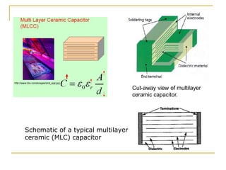
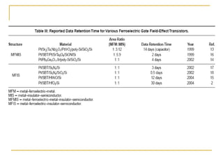
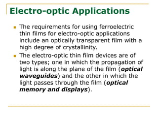
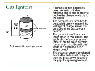
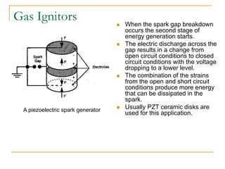
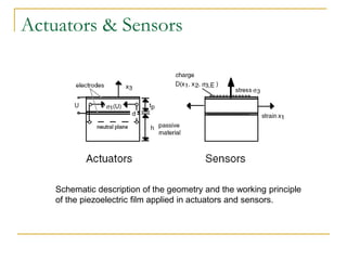
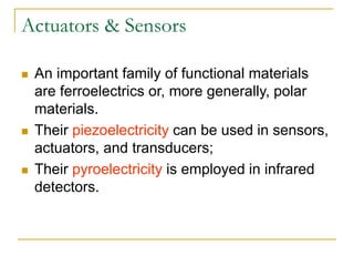
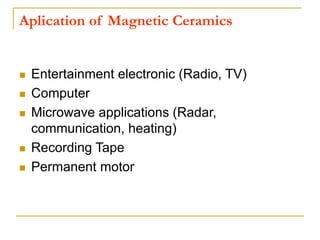
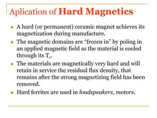
Application of
Electroceramics
EBB 443-Technical Ceramics
Dr. Sabar D. Hutagalung
School of Materials and Mineral Resources Engineering
Universiti Sains Malaysia
Capacitors
 The multilayer ceramic (MLC) capacitors.
 The MLCC structure consists of alternate layers of
dielectric and electrode material.
 Each individual dielectric layer contributes capacitance to
the MLCC as the electrodes terminate in a parallel
configuration.
 The advances in preparation technology have made it
possible to make dielectric layers <1 m thick.
Schematic of a typical multilayer
ceramic (MLC) capacitor
Cut-away view of multilayer
ceramic capacitor.
Applications of Ferroelectric Thin
Films
 Ferroelectric thin films have attracted attention for applications
in many electronic and electro-optic devices.
 Applications of ferroelectric thin films utilize the unique
dielectric, piezoelectric, pyroelectric, and electro-optic
properties of ferroelectric materials.
 Some of the most important electronic applications of
ferroelectric thin films include nonvolatile memories, thin
films capacitors, pyroelectric sensors, and surface acoustic
wave (SAW) substrates.
 The electro-optic devices include optical waveguides and
optical memories and displays.
 Semiconductor memories such as DRAM & SRAM currently
dominate the market.
 However, the disadvantage of these memories is that they are
volatile, i.e. the stored information is lost when the power fails.
 The non-volatile memories available at this time include
complementary metal oxide semiconductors (CMOS) with
battery backup and electrically erasable read only memories
(EEPROM's).
 These non-volatile memories are very expensive.
Ferroelectric Memories
FeRAM Cross Section
FeRAM
 FeRAM is a type of nonvolatile RAM that uses a
ferroelectric film as a capacitor for storing data.
 FeRAM can achieve high-speed read/write
operations comparable to that of DRAM, without
losing data when the power is turned off (unlike
DRAM).
 In addition to nonvolatility and high-speed operation,
FeRAM cells offer the advantages of easy
embedding into VLSI logic circuits and low power
consumption, perhaps their greatest advantage for
many applications.
 FeRAM-embedded VLSI circuits have been
used in
 smart cards,
 radio frequency identification (RFID) tags,
 and as a replacement for BBSRAM (battery
backed-up static RAM), which is used in various
devices to protect data from an unexpected
power failure, as well as in many other SoC
(system on a chip) applications.
FeRAM
 A memory cell, where one bit of data is stored, is
composed of a cell-selection transistor and a capacitor
for 1T1C (one transistor, one capacitor)-type FeRAM.
 A major problem encountered when reducing the size of
the memory cell is preventing reliability degradation.
 The reliability of FeRAM cells is dependent on the
 materials used (ferroelectric film, electrode, interlayer
dielectric, etc.),
 fabrication process,
 device structure,
 memory cell circuit, and
 operation sequence.
FeRAM
Schematic drawings of field-effect transistors (FETs) with
(a) metal–ferroelectric–insulator–semiconductor (MFIS) and
(b) metal–ferroelectric–metal–insulator–semiconductor (MFMIS)
gate structures.
MFIS structures
 The MFIS structure is simple and small in area.
 Thus, it is suitable for high-density integration.
 In an MFIS structure, the effect of the leakage
current is localized around weak spots in the film;
this is important in prolonging the data retention
time.
 In other words, in an MFIS structure, the effect of
the leakage current spreads out to the whole floating
gate, and the charge neutrality is completely
destroyed in a short time. Thus, an MFIS structure is
superior in this regard.
MFMIS structures
 In an MFMIS structure, it is possible to optimize the
area ratio between the ferroelectric and buffer layer
capacitors, so that the induced charges on both
capacitors match.
 In an MFMIS structure, the floating gate material can
be so chosen that a highquality ferroelectric film is
formed on the floating gate and that constituent
elements in the ferroelectric film do not diffuse into
the buffer layer and Si substrate.
Electro-optic Applications
 The requirements for using ferroelectric
thin films for electro-optic applications
include an optically transparent film with a
high degree of crystallinity.
 The electro-optic thin film devices are of
two types; one in which the propagation of
light is along the plane of the film (optical
waveguides) and the other in which the
light passes through the film (optical
memory and displays).
Other Ferroelectric Thin Film
Applications
Thin Film Capacitors:
 The high dielectric permittivity of ferroelectric ceramics
such as BaTiO3, PMN and PZT very useful for capacitor
applications.
 The MLC capacitors have a very high volumetric
efficiency (capacitance per unit volume) because of the
combined capacitance of thin ceramic tapes (~ 10-20 m m)
stacked one on top of the other.
Pyroelectric Detectors :
 Pyroelectricity is the polarization produced due to a small
change in temperature.
 Single crystals of triglycine sulfate (TGS), LiTaO3, and
(Sr,Ba)Nb2O6 are widely used for heat sensing
applications.
 PbTiO3, (Pb,La)TiO3 and PZT have been widely studied
for thin film pyroelectric sensing applications.
Surface Acoustic Wave Substrates :
 SAW devices are fabricated by depositing interdigital
electrodes on the surface of a piezoelectric substrate.
 An elastic wave generated at the input interdigital
transducer (IDT) travels along the surface of the
piezoelectric substrate and it is detected by the output
interdigital transducer.
 These devices are mainly used for delay lines and filters in
television and microwave communication applications.
Schematic representation of the generation,
propagation and detection of surface acoustic
waves (SAW) on a piezoelectric substrate with
interdigital electrode.
Gas Ignitors  It consists of two oppositely
poled ceramic cylinders
attached end to end in order to
double the charge available for
the spark.
 The compressive force has to
be applied quickly to avoid the
leakage of charge across the
surfaces of the piezoelectric
ceramic.
 The generation of the spark
takes place in two stages. The
application of a compressive
force 'F' on the poled ceramic
(under open circuit conditions)
leads to a decrease in the
length by dLD.
 The potential energy developed
across the ends must be higher
than the breakdown voltage of
the gap, for sparking to occur.
A piezoelectric spark generator
Gas Ignitors  When the spark gap breakdown
occurs the second stage of
energy generation starts.
 The electric discharge across the
gap results in a change from
open circuit conditions to closed
circuit conditions with the voltage
dropping to a lower level.
 The combination of the strains
from the open and short circuit
conditions produce more energy
that can be dissipated in the
spark.
 Usually PZT ceramic disks are
used for this application.
A piezoelectric spark generator
Actuators & Sensors
Schematic description of the geometry and the working principle
of the piezoelectric film applied in actuators and sensors.
Actuators & Sensors
 An important family of functional materials
are ferroelectrics or, more generally, polar
materials.
 Their piezoelectricity can be used in sensors,
actuators, and transducers;
 Their pyroelectricity is employed in infrared
detectors.
Piezoelectric Microactuator Devices
Schematic draw of optical scanning device
with double layered PZT layer (a) and the
fabricated device, (b) Mirror plate: 300×300
(µm2, DPZT beam: 800 × 230 µm2).
Schematic drawing of self-actuation
cantilever with an integrated
piezoresistor.
Micropump using screen-printed PZT
actuator on silicon membrane.
(Courtesy of Neil White, Univ. of
Southampton, UK.)
Aplication of Magnetic Ceramics
 Entertainment electronic (Radio, TV)
 Computer
 Microwave applications (Radar,
communication, heating)
 Recording Tape
 Permanent motor
Aplication of Magnetic Ceramics
 Spinel (cubic ferrites): Soft magnets
 Garnet (rare earth ferrites): Microwave devices
 Magnetoplumbite (hexagonal ferrites): Hard
magnets
Aplication of Soft Magnetics
 In the soft magnetic materials, only a small field is
necessary to cause demagnetization and very small
energy losses occur per cycle of hysteresis loop.
 This is important for applications such as
transformers used in touch tone telephones or
inductors or magnetic memory cores.
 During used a soft ferrites has its magnetic domains
rapidly and easily realigned by the changing
magnetic field.
Aplication of Hard Magnetics
 A hard (or permanent) ceramic magnet achieves its
magnetization during manufacture.
 The magnetic domains are “frozen in” by poling in
an applied magnetic field as the material is cooled
through its Tc.
 The materials are magnetically very hard and will
retain in service the residual flux density, that
remains after the strong magnetizing field has been
removed.
 Hard ferrites are used in loudspeakers, motors.
Aplication of Ferrites
 The cubic spinels, also called ferrospinels, are
used as soft magnetic materials because of their
very low coercive force of 4x10⁻⁵ weber/m2 and high
saturation magnetization 0.3-0.4 weber/m2.
(1 weber = 1 volt-second = 108 Maxwells)
 Flux density (induction): 1 Tesla = 104 Gauss = 1
weber/m2. (1 Gauss = 1 Maxwell/cm2).
 Hexagonal ferrites are hard magnetic materials with
coercive force of 0.2 – 0.4 weber/m2 and large
resistance to demagnetization, 2 – 3 J/m3.
Aplication of Garnets
 Garnets are especially suited for high frequency
microwave applications due to the ability to tailor
properties such as magnetization, line width, g-
factor, Tc, and temperature stability.
 The most common garnet ferrites are based upon
3Y2O3 : 5Fe2O3 or Y3Fe5O12 or YIG.
Tape Recording
 Before passing over the record head,
a tape passes over the erase head
which applies a high amplitude, high
frequency magnetic field to the tape
to erase any previously recorded
signal and to thoroughly randomize
the magnetization of the magnetic
emulsion.
 The gap in the erase head is wider
than those in the record head; the
tape stays in the field of the head
longer to thoroughly erase any
previously recorded signal.
Tape Recording
 High fidelity tape recording requires a high frequency
biasing signal to be applied to the tape head along with
the signal to "stir" the magnetization of the tape .
 This is because magnetic tapes are very sensitive to their
previous magnetic history, a property called hysteresis.
 A magnetic "image" of a sound signal can be stored on
tape in the form of magnetized iron oxide or chromium
dioxide granules in a magnetic emulsion.
 The tiny granules are fixed on a polyester film base, but
the direction and extent of their magnetization can be
changed to record an input signal from a tape head.
Electromagnet
 Electromagnets are usually in the form of iron core
solenoids.
 The ferromagnetic property of the iron core causes
the internal magnetic domains of the iron to line up
with the smaller driving magnetiv field driving
produced by the current in the solenoid.
 The solenoid field relationship is
and k is the relative permeability of the iron, shows
the magnifying effect of the iron core.
Transformer
 A transformer makes use of Faraday’s law and the
ferromagnetic properties of an iron core to efficiently
raise or lower AC voltages.
 It of course cannot increase power so that if the voltage
is raised, the current is proportionally lowered and vice
versa.
Transformer
Applications of GMR
 The largest technological application of GMR is in the data
storage industry.
 IBM were first to market with hard disks based on GMR
technology although today all disk drives make use of this
technology.
 On-chip GMR sensors are available commercially from
Non-Volatile Electronics.
 It is expected that the GMR effect will allow disk drive
manufacturers to continue increasing density at least until
disk capacity reaches 10 Gb per square inch.
 At this density, 120 billion bits could be stored on a typical
3.5-inch disk drive, or the equivalent of about a thousand
30-volume encyclopedias.
Applications of GMR
 Other applications are as diverse as solid-state
compasses, automotive sensors, non-volatile
magnetic memory and the detection of landmines.
Applications of GMR
 GMR also may spur the replacement of RAM in
computers with magnetic RAM (MRAM).
 Using GMR, it may be possible to make thin-film MRAM
that would be just as fast, dense, and inexpensive.
 It would have the additional advantages of being
nonvolatile and radiation-resistant.
 Data would not be lost if the power failed unexpectedly,
and the device would continue to function in the
presence of ionizing radiation, making it useful for
space and defense applications.
Applications of GMR
 Reading and writing with a magnetoresistive probe.
 C B Craus, T Onoue, K Ramstock,W G M A Geerts, M H Siekman, L Abelmann
and J C Lodder, J. Phys. D: Appl. Phys. 38 (2005) 363–370
Application of Superconductors
Power lines.
 A significant amount of electrical energy is wasted as heat
when electricity is transmitted down cables made of traditional
metal conductors.
 Superconductors, can conduct electricity with zero resistance
and would therefore be more efficient.
Transport.
 Magnetically levitated trains already exist.
 Using superconducting magnets, cheaper, faster and more
efficient variants could be produced.
Electronics.
 By harnessing the Josephson effect, extremely fast electronic
switches could be constructed, allowing faster
microprocessors to be built.
Microwave Dielectrics
 The Microwave materials including of dielectric and
coaxial resonators to meet the demands of microwave
applications for high performance, low cost devices in
small, medium and large quantities.
 Applications
 Patch antennas
 Resonators /inductors
 Substrates
 C-band resonator-mobile
 Filters
Dielectric Resonator (DR)
 Used in shielded microwave circuits,
such as cavity resonator, filters and
oscillators.
 Application: as antenna in microwave
and millimeter band.
 Advantages of DR:
 light weight, low cost, small size,
high radiation efficiency, large
bandwidth.
High-K dielectric to reduce size
 Dielectric Resonator (DR)
size is inversely proportional
to the frequency:
 Larger , lower frequency
 Larger , smaller size

L
c
f
2

 Photograph of split post dielectric resonators
operating at frequencies: 1.4, 3.2 and 33 GHz.
Jerzy Krupka, Journal of the European Ceramic Society 23 (2003) 2607–2610
Super-K CCTO

applications.ppt

  • 1.
    Application of Electroceramics EBB 443-TechnicalCeramics Dr. Sabar D. Hutagalung School of Materials and Mineral Resources Engineering Universiti Sains Malaysia
  • 2.
    Capacitors  The multilayerceramic (MLC) capacitors.  The MLCC structure consists of alternate layers of dielectric and electrode material.  Each individual dielectric layer contributes capacitance to the MLCC as the electrodes terminate in a parallel configuration.  The advances in preparation technology have made it possible to make dielectric layers <1 m thick.
  • 3.
    Schematic of atypical multilayer ceramic (MLC) capacitor Cut-away view of multilayer ceramic capacitor.
  • 4.
    Applications of FerroelectricThin Films  Ferroelectric thin films have attracted attention for applications in many electronic and electro-optic devices.  Applications of ferroelectric thin films utilize the unique dielectric, piezoelectric, pyroelectric, and electro-optic properties of ferroelectric materials.  Some of the most important electronic applications of ferroelectric thin films include nonvolatile memories, thin films capacitors, pyroelectric sensors, and surface acoustic wave (SAW) substrates.  The electro-optic devices include optical waveguides and optical memories and displays.
  • 5.
     Semiconductor memoriessuch as DRAM & SRAM currently dominate the market.  However, the disadvantage of these memories is that they are volatile, i.e. the stored information is lost when the power fails.  The non-volatile memories available at this time include complementary metal oxide semiconductors (CMOS) with battery backup and electrically erasable read only memories (EEPROM's).  These non-volatile memories are very expensive. Ferroelectric Memories
  • 6.
  • 7.
    FeRAM  FeRAM isa type of nonvolatile RAM that uses a ferroelectric film as a capacitor for storing data.  FeRAM can achieve high-speed read/write operations comparable to that of DRAM, without losing data when the power is turned off (unlike DRAM).  In addition to nonvolatility and high-speed operation, FeRAM cells offer the advantages of easy embedding into VLSI logic circuits and low power consumption, perhaps their greatest advantage for many applications.
  • 8.
     FeRAM-embedded VLSIcircuits have been used in  smart cards,  radio frequency identification (RFID) tags,  and as a replacement for BBSRAM (battery backed-up static RAM), which is used in various devices to protect data from an unexpected power failure, as well as in many other SoC (system on a chip) applications. FeRAM
  • 9.
     A memorycell, where one bit of data is stored, is composed of a cell-selection transistor and a capacitor for 1T1C (one transistor, one capacitor)-type FeRAM.  A major problem encountered when reducing the size of the memory cell is preventing reliability degradation.  The reliability of FeRAM cells is dependent on the  materials used (ferroelectric film, electrode, interlayer dielectric, etc.),  fabrication process,  device structure,  memory cell circuit, and  operation sequence. FeRAM
  • 10.
    Schematic drawings offield-effect transistors (FETs) with (a) metal–ferroelectric–insulator–semiconductor (MFIS) and (b) metal–ferroelectric–metal–insulator–semiconductor (MFMIS) gate structures.
  • 11.
    MFIS structures  TheMFIS structure is simple and small in area.  Thus, it is suitable for high-density integration.  In an MFIS structure, the effect of the leakage current is localized around weak spots in the film; this is important in prolonging the data retention time.  In other words, in an MFIS structure, the effect of the leakage current spreads out to the whole floating gate, and the charge neutrality is completely destroyed in a short time. Thus, an MFIS structure is superior in this regard.
  • 12.
    MFMIS structures  Inan MFMIS structure, it is possible to optimize the area ratio between the ferroelectric and buffer layer capacitors, so that the induced charges on both capacitors match.  In an MFMIS structure, the floating gate material can be so chosen that a highquality ferroelectric film is formed on the floating gate and that constituent elements in the ferroelectric film do not diffuse into the buffer layer and Si substrate.
  • 16.
    Electro-optic Applications  Therequirements for using ferroelectric thin films for electro-optic applications include an optically transparent film with a high degree of crystallinity.  The electro-optic thin film devices are of two types; one in which the propagation of light is along the plane of the film (optical waveguides) and the other in which the light passes through the film (optical memory and displays).
  • 17.
    Other Ferroelectric ThinFilm Applications Thin Film Capacitors:  The high dielectric permittivity of ferroelectric ceramics such as BaTiO3, PMN and PZT very useful for capacitor applications.  The MLC capacitors have a very high volumetric efficiency (capacitance per unit volume) because of the combined capacitance of thin ceramic tapes (~ 10-20 m m) stacked one on top of the other.
  • 18.
    Pyroelectric Detectors : Pyroelectricity is the polarization produced due to a small change in temperature.  Single crystals of triglycine sulfate (TGS), LiTaO3, and (Sr,Ba)Nb2O6 are widely used for heat sensing applications.  PbTiO3, (Pb,La)TiO3 and PZT have been widely studied for thin film pyroelectric sensing applications.
  • 19.
    Surface Acoustic WaveSubstrates :  SAW devices are fabricated by depositing interdigital electrodes on the surface of a piezoelectric substrate.  An elastic wave generated at the input interdigital transducer (IDT) travels along the surface of the piezoelectric substrate and it is detected by the output interdigital transducer.  These devices are mainly used for delay lines and filters in television and microwave communication applications.
  • 20.
    Schematic representation ofthe generation, propagation and detection of surface acoustic waves (SAW) on a piezoelectric substrate with interdigital electrode.
  • 21.
    Gas Ignitors It consists of two oppositely poled ceramic cylinders attached end to end in order to double the charge available for the spark.  The compressive force has to be applied quickly to avoid the leakage of charge across the surfaces of the piezoelectric ceramic.  The generation of the spark takes place in two stages. The application of a compressive force 'F' on the poled ceramic (under open circuit conditions) leads to a decrease in the length by dLD.  The potential energy developed across the ends must be higher than the breakdown voltage of the gap, for sparking to occur. A piezoelectric spark generator
  • 22.
    Gas Ignitors When the spark gap breakdown occurs the second stage of energy generation starts.  The electric discharge across the gap results in a change from open circuit conditions to closed circuit conditions with the voltage dropping to a lower level.  The combination of the strains from the open and short circuit conditions produce more energy that can be dissipated in the spark.  Usually PZT ceramic disks are used for this application. A piezoelectric spark generator
  • 23.
    Actuators & Sensors Schematicdescription of the geometry and the working principle of the piezoelectric film applied in actuators and sensors.
  • 24.
    Actuators & Sensors An important family of functional materials are ferroelectrics or, more generally, polar materials.  Their piezoelectricity can be used in sensors, actuators, and transducers;  Their pyroelectricity is employed in infrared detectors.
  • 25.
    Piezoelectric Microactuator Devices Schematicdraw of optical scanning device with double layered PZT layer (a) and the fabricated device, (b) Mirror plate: 300×300 (µm2, DPZT beam: 800 × 230 µm2). Schematic drawing of self-actuation cantilever with an integrated piezoresistor. Micropump using screen-printed PZT actuator on silicon membrane. (Courtesy of Neil White, Univ. of Southampton, UK.)
  • 26.
    Aplication of MagneticCeramics  Entertainment electronic (Radio, TV)  Computer  Microwave applications (Radar, communication, heating)  Recording Tape  Permanent motor
  • 27.
    Aplication of MagneticCeramics  Spinel (cubic ferrites): Soft magnets  Garnet (rare earth ferrites): Microwave devices  Magnetoplumbite (hexagonal ferrites): Hard magnets
  • 28.
    Aplication of SoftMagnetics  In the soft magnetic materials, only a small field is necessary to cause demagnetization and very small energy losses occur per cycle of hysteresis loop.  This is important for applications such as transformers used in touch tone telephones or inductors or magnetic memory cores.  During used a soft ferrites has its magnetic domains rapidly and easily realigned by the changing magnetic field.
  • 29.
    Aplication of HardMagnetics  A hard (or permanent) ceramic magnet achieves its magnetization during manufacture.  The magnetic domains are “frozen in” by poling in an applied magnetic field as the material is cooled through its Tc.  The materials are magnetically very hard and will retain in service the residual flux density, that remains after the strong magnetizing field has been removed.  Hard ferrites are used in loudspeakers, motors.
  • 30.
    Aplication of Ferrites The cubic spinels, also called ferrospinels, are used as soft magnetic materials because of their very low coercive force of 4x10⁻⁵ weber/m2 and high saturation magnetization 0.3-0.4 weber/m2. (1 weber = 1 volt-second = 108 Maxwells)  Flux density (induction): 1 Tesla = 104 Gauss = 1 weber/m2. (1 Gauss = 1 Maxwell/cm2).  Hexagonal ferrites are hard magnetic materials with coercive force of 0.2 – 0.4 weber/m2 and large resistance to demagnetization, 2 – 3 J/m3.
  • 31.
    Aplication of Garnets Garnets are especially suited for high frequency microwave applications due to the ability to tailor properties such as magnetization, line width, g- factor, Tc, and temperature stability.  The most common garnet ferrites are based upon 3Y2O3 : 5Fe2O3 or Y3Fe5O12 or YIG.
  • 32.
    Tape Recording  Beforepassing over the record head, a tape passes over the erase head which applies a high amplitude, high frequency magnetic field to the tape to erase any previously recorded signal and to thoroughly randomize the magnetization of the magnetic emulsion.  The gap in the erase head is wider than those in the record head; the tape stays in the field of the head longer to thoroughly erase any previously recorded signal.
  • 33.
    Tape Recording  Highfidelity tape recording requires a high frequency biasing signal to be applied to the tape head along with the signal to "stir" the magnetization of the tape .  This is because magnetic tapes are very sensitive to their previous magnetic history, a property called hysteresis.  A magnetic "image" of a sound signal can be stored on tape in the form of magnetized iron oxide or chromium dioxide granules in a magnetic emulsion.  The tiny granules are fixed on a polyester film base, but the direction and extent of their magnetization can be changed to record an input signal from a tape head.
  • 34.
    Electromagnet  Electromagnets areusually in the form of iron core solenoids.  The ferromagnetic property of the iron core causes the internal magnetic domains of the iron to line up with the smaller driving magnetiv field driving produced by the current in the solenoid.  The solenoid field relationship is and k is the relative permeability of the iron, shows the magnifying effect of the iron core.
  • 35.
    Transformer  A transformermakes use of Faraday’s law and the ferromagnetic properties of an iron core to efficiently raise or lower AC voltages.  It of course cannot increase power so that if the voltage is raised, the current is proportionally lowered and vice versa.
  • 36.
  • 37.
    Applications of GMR The largest technological application of GMR is in the data storage industry.  IBM were first to market with hard disks based on GMR technology although today all disk drives make use of this technology.  On-chip GMR sensors are available commercially from Non-Volatile Electronics.  It is expected that the GMR effect will allow disk drive manufacturers to continue increasing density at least until disk capacity reaches 10 Gb per square inch.  At this density, 120 billion bits could be stored on a typical 3.5-inch disk drive, or the equivalent of about a thousand 30-volume encyclopedias.
  • 38.
    Applications of GMR Other applications are as diverse as solid-state compasses, automotive sensors, non-volatile magnetic memory and the detection of landmines.
  • 39.
    Applications of GMR GMR also may spur the replacement of RAM in computers with magnetic RAM (MRAM).  Using GMR, it may be possible to make thin-film MRAM that would be just as fast, dense, and inexpensive.  It would have the additional advantages of being nonvolatile and radiation-resistant.  Data would not be lost if the power failed unexpectedly, and the device would continue to function in the presence of ionizing radiation, making it useful for space and defense applications.
  • 40.
    Applications of GMR Reading and writing with a magnetoresistive probe.  C B Craus, T Onoue, K Ramstock,W G M A Geerts, M H Siekman, L Abelmann and J C Lodder, J. Phys. D: Appl. Phys. 38 (2005) 363–370
  • 41.
    Application of Superconductors Powerlines.  A significant amount of electrical energy is wasted as heat when electricity is transmitted down cables made of traditional metal conductors.  Superconductors, can conduct electricity with zero resistance and would therefore be more efficient. Transport.  Magnetically levitated trains already exist.  Using superconducting magnets, cheaper, faster and more efficient variants could be produced. Electronics.  By harnessing the Josephson effect, extremely fast electronic switches could be constructed, allowing faster microprocessors to be built.
  • 42.
    Microwave Dielectrics  TheMicrowave materials including of dielectric and coaxial resonators to meet the demands of microwave applications for high performance, low cost devices in small, medium and large quantities.  Applications  Patch antennas  Resonators /inductors  Substrates  C-band resonator-mobile  Filters
  • 43.
    Dielectric Resonator (DR) Used in shielded microwave circuits, such as cavity resonator, filters and oscillators.  Application: as antenna in microwave and millimeter band.  Advantages of DR:  light weight, low cost, small size, high radiation efficiency, large bandwidth.
  • 44.
    High-K dielectric toreduce size  Dielectric Resonator (DR) size is inversely proportional to the frequency:  Larger , lower frequency  Larger , smaller size  L c f 2 
  • 45.
     Photograph ofsplit post dielectric resonators operating at frequencies: 1.4, 3.2 and 33 GHz. Jerzy Krupka, Journal of the European Ceramic Society 23 (2003) 2607–2610
  • 46.