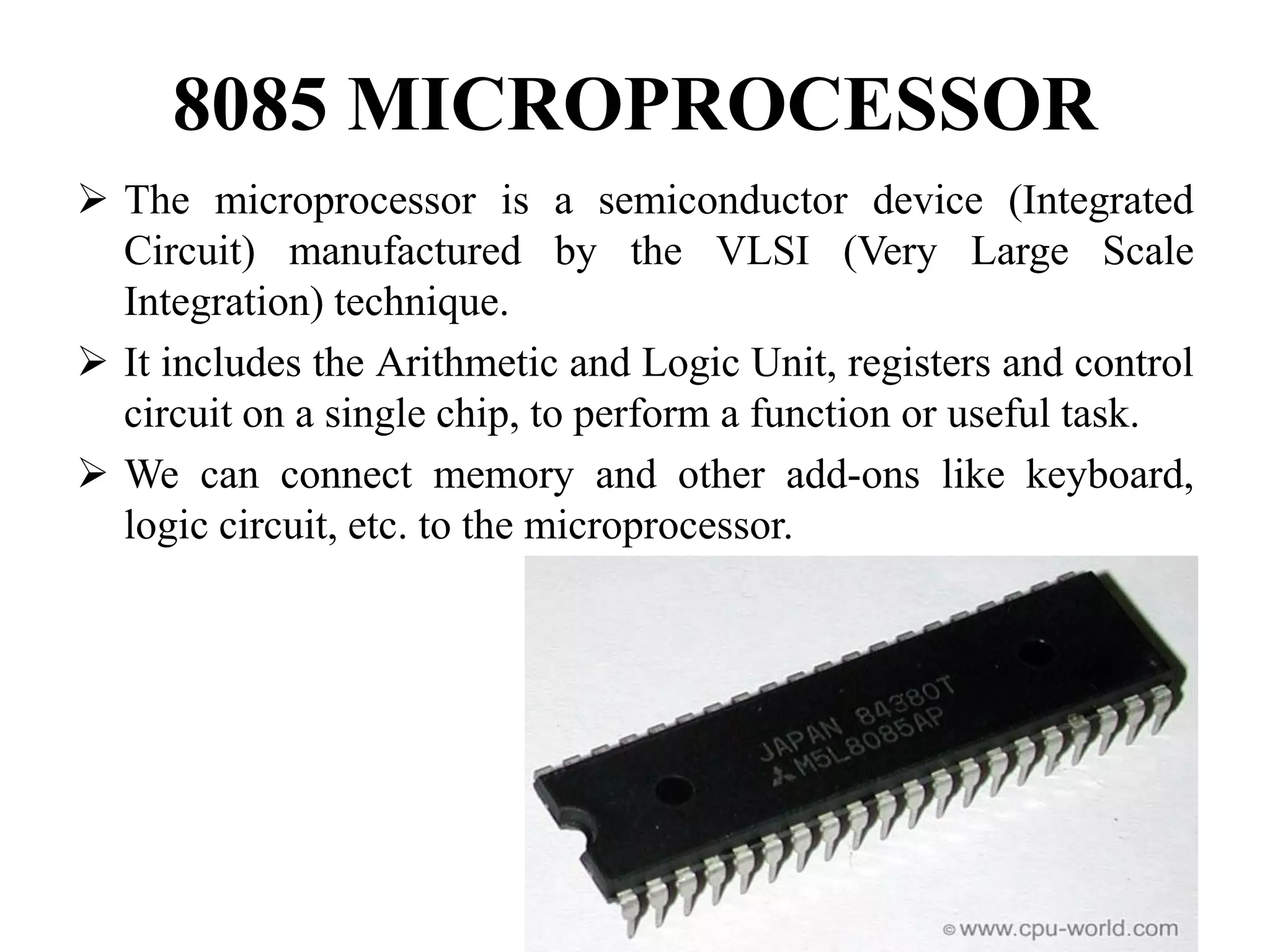
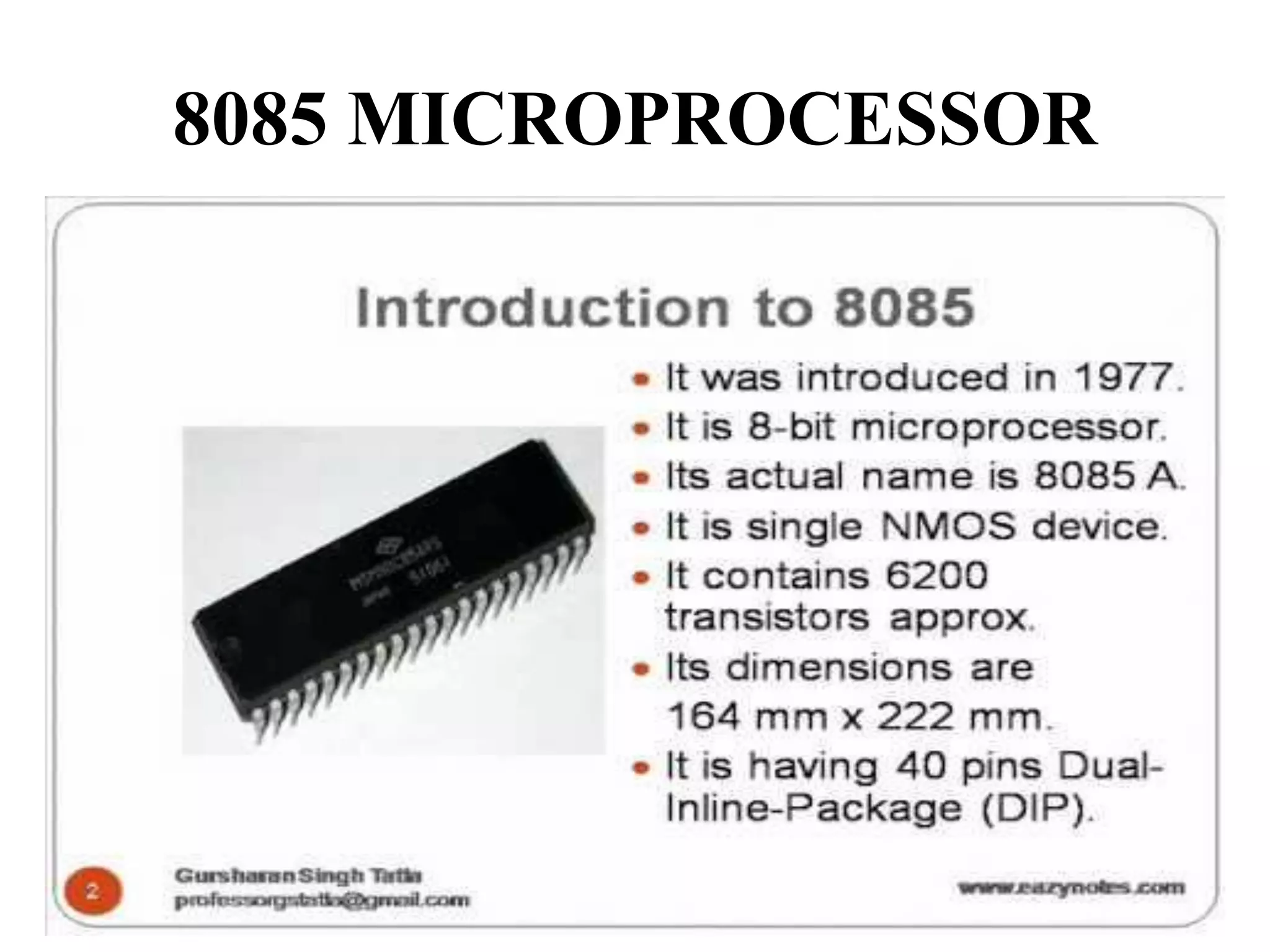
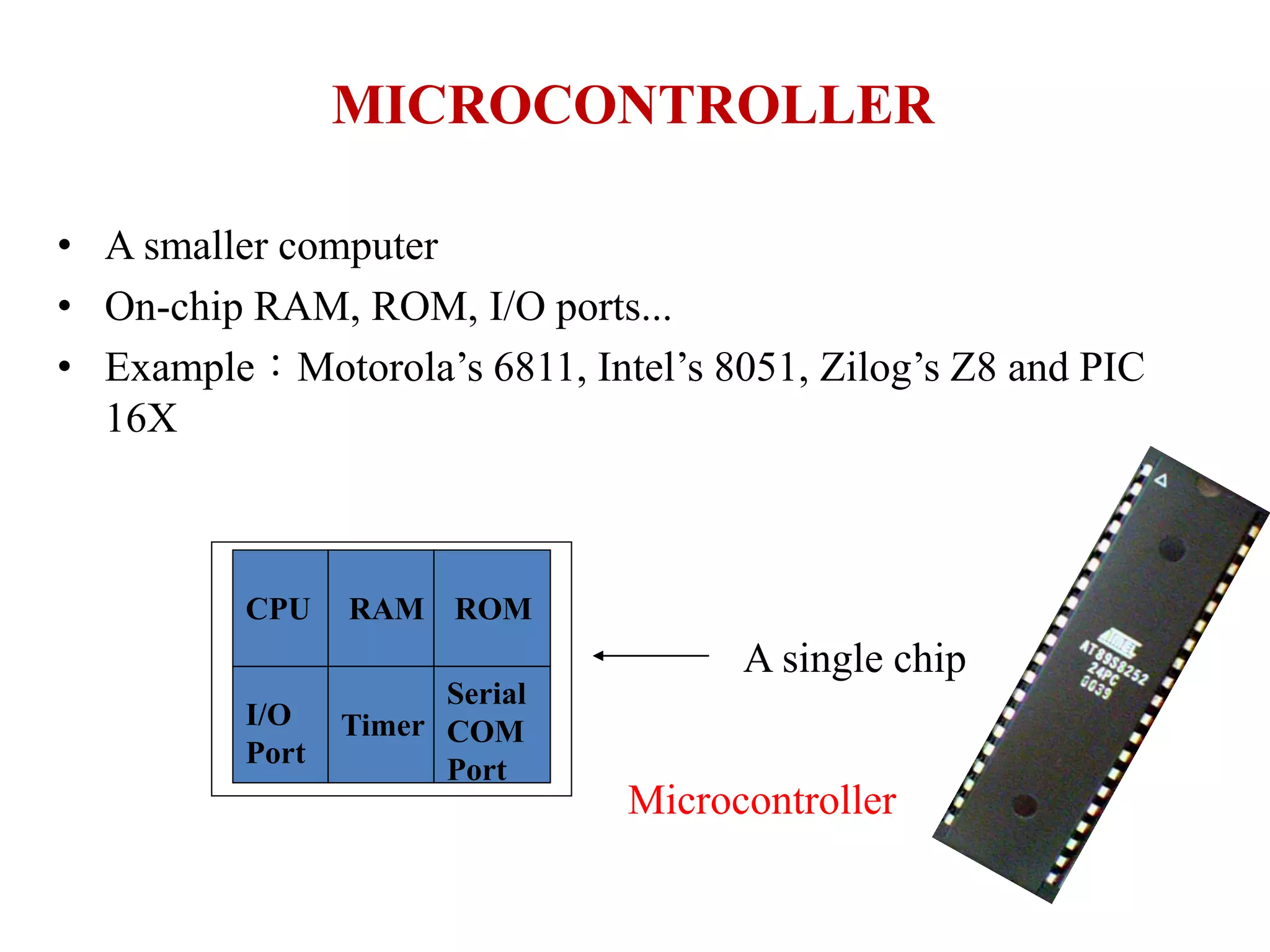
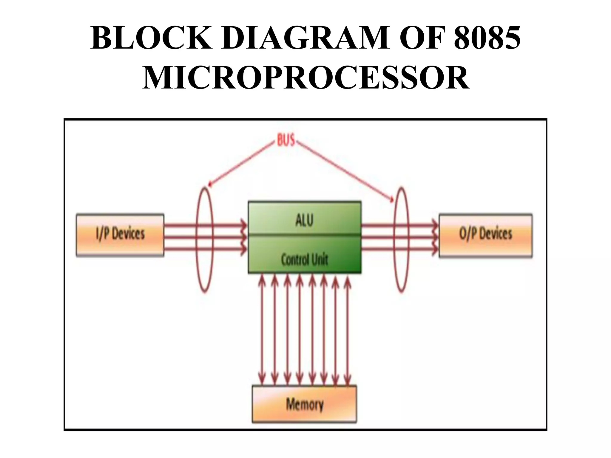
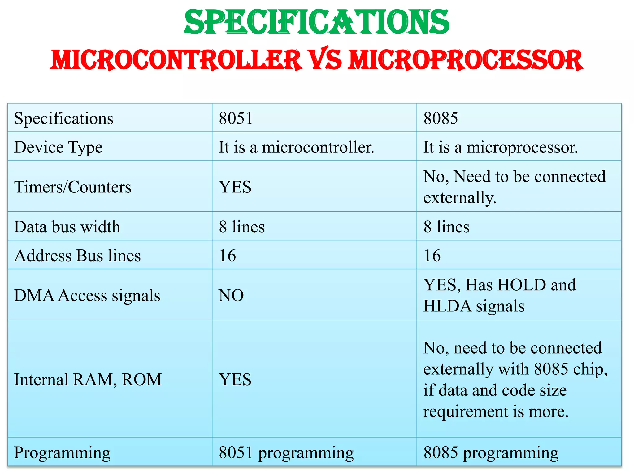
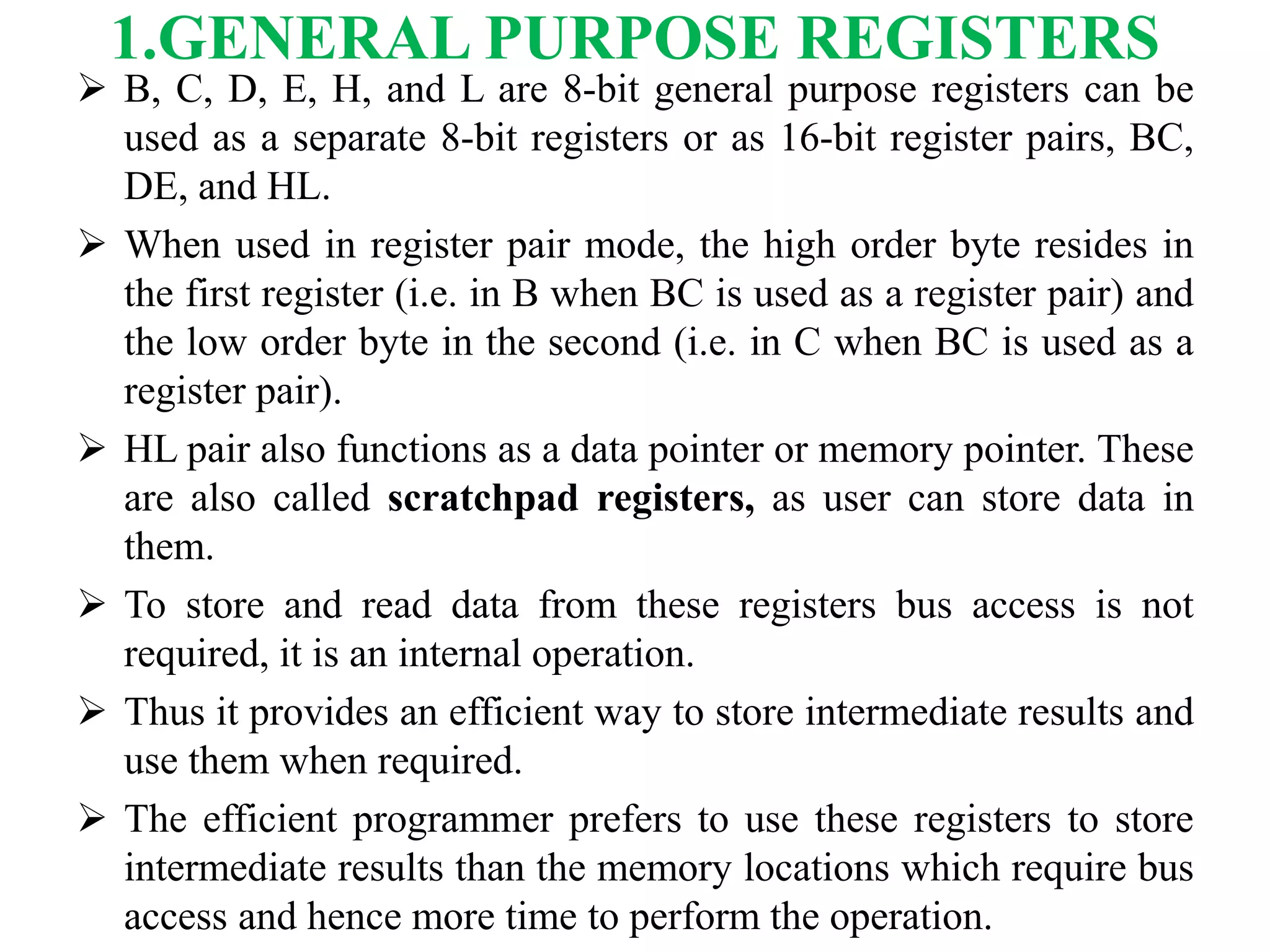
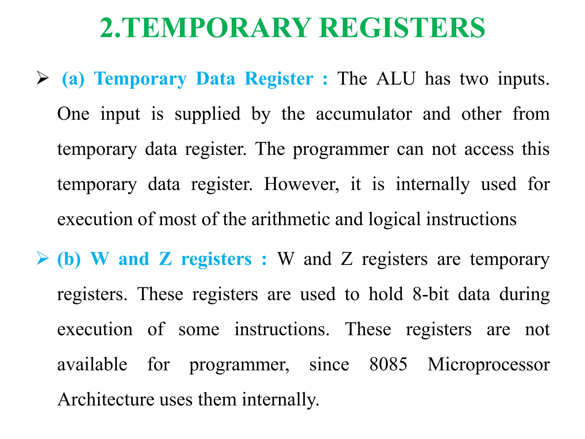
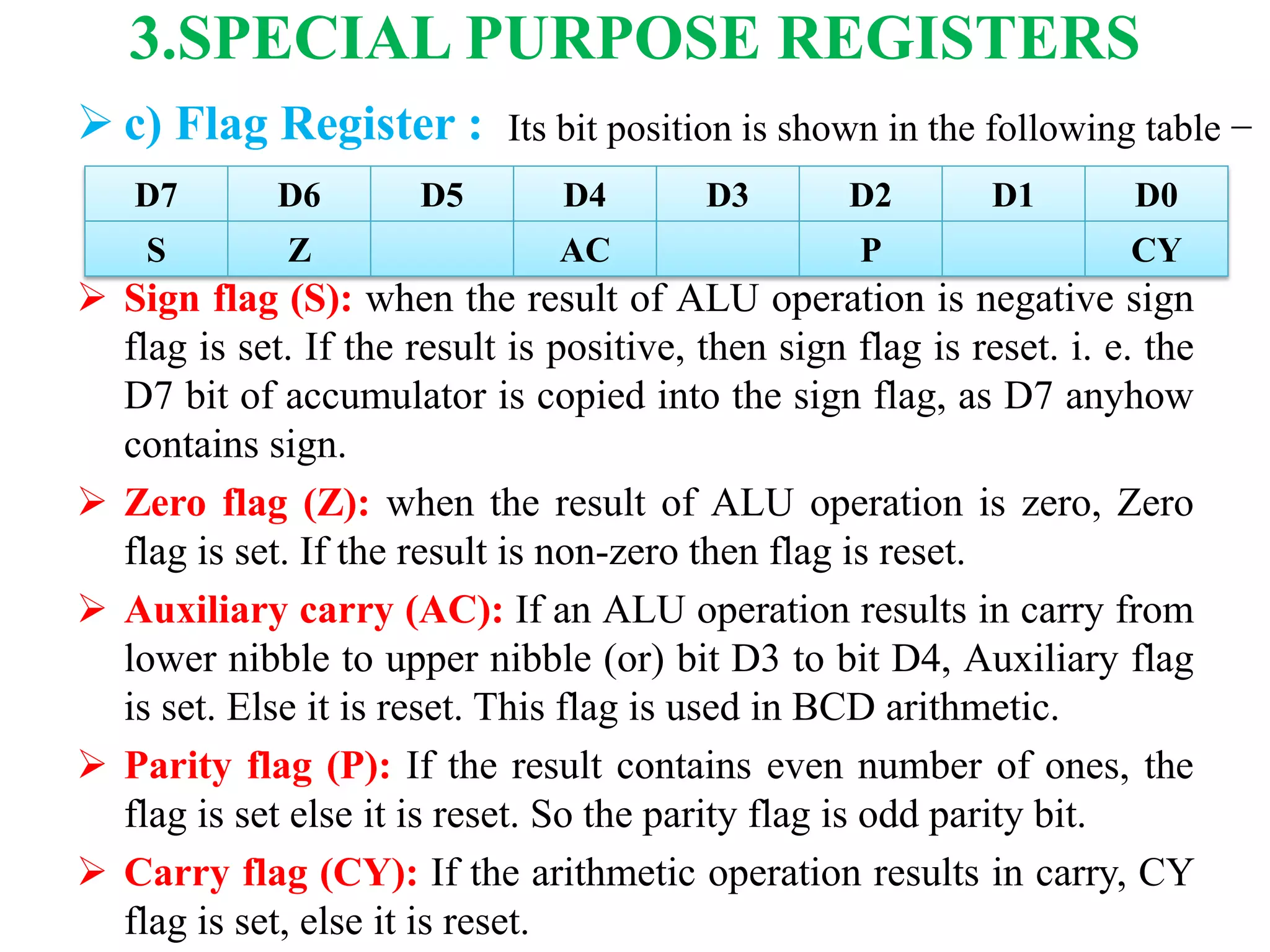
SlideShare a Scribd company logo
UNIT-IIi
8085 MICROPROCESSOR &
8051 MICROCONTROLLER
LECTURE-1
 INTRODUCTION
8085 MICROPROCESSOR
 The microprocessor is a semiconductor device (Integrated
Circuit) manufactured by the VLSI (Very Large Scale
Integration) technique.
 It includes the Arithmetic and Logic Unit, registers and control
circuit on a single chip, to perform a function or useful task.
 We can connect memory and other add-ons like keyboard,
logic circuit, etc. to the microprocessor.
8085 MICROPROCESSOR
 The microprocessor then commands these devices to
act according to the program or code written in it.
 Inside the microprocessor there is a Central Processing
Unit, semiconductor memories like EPROM and RAM,
input device, output device and interfacing devices.
 The memories, input device, output device and
interfacing devices are called peripherals.
 The popular input devices are keyboard and floppy disk
and the output devices are printer, LED/LCD displays,
CRT monitor, etc.
8085 MICROPROCESSOR
What is the Microprocessor?
A microprocessor, sometimes called a logic chip,
is a computer processor on a microchip.
 The microprocessor contains all, or most of, the
central processing unit (CPU) functions and is the
"engine" that goes into motion when you turn
your computer on.
8085 is pronounced as "eighty-eighty-five"
microprocessor. It is an 8-bit microprocessor
designed by Intel in 1977 using NMOS
technology.
8051 MICROCONTROLLER
 A microcontroller is a computer present in a single
integrated circuit which is dedicated to perform one
task and execute one specific application.
 It contains memory, programmable input/output
peripherals as well a processor.
 The Intel 8051 is an 8-bit microcontroller which
means that most available operations are limited to 8
bits.
Why do we need to learn
8051 microcontroller?
 Its not an exaggeration if I say that ,today there is no
electronic gadget on the earth which is designed
without a Microcontroller.
 Ex: communication devices, digital entertainment,
portable devices etc…
APPLICATIONS OF 8051
 Personal information products: Cell phone, pager,
watch, pocket recorder, calculator
 Laptop components: mouse, keyboard, modem, fax
card, sound card, battery charger
 Home appliances: door lock, alarm clock,
thermostat, air conditioner, TV remote, VCR, small
refrigerator, exercise equipment, washer/dryer,
microwave oven
 Industrial equipment: Temperature/pressure controllers,
Counters, timers, RPM Controllers
 Toys: video games, cars, dolls, etc.
What is the microcontroller?
 A Microcontroller is a VLSI IC that contains a CPU
(Processor) along with some other peripherals like
Memory (RAM and ROM), I/O Ports,
Timers/Counters, Communication Interface, ADC,
etc.
MICROPROCESSOR
vs
MICROCONTROLLER
Thursday, October 22, 2020 Mahdi Hassanpour
CPU
General-
Purpose
Micro-
processor
RAM ROM I/O
Port
Timer
Serial
COM
Port
Data Bus
Address Bus
General-Purpose Microprocessor System
 CPU for Computers
 No RAM, ROM, I/O on CPU chip itself
 Example:Intel’s x86, Motorola’s 680x0
Many chips on mother’s board
MICROPROCESSOR
Thursday, October 22, 2020 Mahdi Hassanpour
RAM ROM
I/O
Port
Timer
Serial
COM
Port
Microcontroller
CPU
• A smaller computer
• On-chip RAM, ROM, I/O ports...
• Example:Motorola’s 6811, Intel’s 8051, Zilog’s Z8 and PIC
16X
A single chip
MICROCONTROLLER
Thursday, October 22, 2020 Mahdi Hassanpour
Microprocessor
• CPU is stand-alone, RAM,
ROM, I/O, timer are separate
• designer can decide on the
amount of ROM, RAM and I/O
ports.
• expansive
• versatility
• general-purpose
Microcontroller
• CPU, RAM, ROM, I/O and
timer are all on a single chip
• fix amount of on-chip ROM,
RAM, I/O ports
• for applications in which cost,
power and space are critical
• single-purpose
MICROPROCESSOR vs MICROCONTROLLER
SAliENT FEATURES
MICROPROCESSOR vs MICROCONTROLLER
 8-bit data bus
 16-bit address bus, which can
address upto 64KB
 A 16-bit program counter
 A 16-bit stack pointer
 Six 8-bit registers arranged in
pairs: BC, DE, HL
 Requires +5V supply to operate at
3.2 MHZ single phase clock
 The maximum clock frequency
used in 8085 is 3 MHz.
 It has two serial lines viz SID and
SOD.
 It consists of ACC, one flag
register, 6 general purpose
registers and 2 special registers.
 64K bytes on-chip program
memory (ROM)
 128 bytes on-chip data memory
(RAM)
 Four register banks
 128 user defined software flags
 8-bit bidirectional data bus
 16-bit unidirectional address bus
 32 general purpose registers
 16 bit Timers
 Three internal and two external
Interrupts
 Four 8-bit ports
 16-bit program counter and data
pointer
BLOCK DIAGRAM OF 8085
MICROPROCESSOR
BLOCK DIAGRAM OF 8051
MICROCONTROLLER
Specifications
MICROCONTROLLER vs MICROPROCESSOR
Specifications 8051 8085
Device Type It is a microcontroller. It is a microprocessor.
Timers/Counters YES
No, Need to be connected
externally.
Data bus width 8 lines 8 lines
Address Bus lines 16 16
DMAAccess signals NO
YES, Has HOLD and
HLDA signals
Internal RAM, ROM YES
No, need to be connected
externally with 8085 chip,
if data and code size
requirement is more.
Programming 8051 programming 8085 programming
LECTURE-2
 ARCHITECHTURE OF 8085
ARCHITECTURE OF 8085
MICROPROCESSOR
What is the architecture of a microprocessor?
A microprocessor is a computer processor
that incorporates the functions of a central processing
unit on a single integrated circuit (IC), or at most a few
integrated circuits. ... Microprocessors combined this
into one or a few large-scale ICs.
SALIENT FEATURES OF MICROPROCESSOR
 8-bit data bus
 16-bit address bus, which can address upto 64KB
 A 16-bit program counter
 A 16-bit stack pointer
 Six 8-bit registers arranged in pairs: BC, DE, HL
 Requires +5V supply to operate at 3.2 MHZ single phase clock
 The maximum clock frequency used in 8085 is 3 MHz.
 It has two serial lines viz SID and SOD.
 It consists of ACC, one flag register, 6 general purpose registers and 2 special
registers
Mahdi Hassanpour
FUNCTIONAL BLOCKS OF 8085
It consists of various functional blocks as listed below :
 Registers
 Arithmetic and Logic Unit
 Instruction decoder and machine cycle encoder
 Address buffer
 Address/Data buffer
 Incrementer/Decrementer Address Latch
 Interrupt control
 Serial I/O control
 Timing and control circuitry.
ARCHITECTURE OF 8085 MICROPROCESSOR
REGISTERS
It has eight addressable 8-bit registers : A, B,
C, D, E, H, L, F, and two 16-bit registers PC and SP.
These registers can be classified as:
I. General Purpose Registers
II. Temporary Registers:
a) Temporary data register
b) W and Z registers
III. Special Purpose Registers:
a) Accumulator
b) Flag registers
c) Instruction register
IV. Sixteen bit Registers:
a) Program counter(PC)
b) Stack Pointer (SP)
1.GENERAL PURPOSE REGISTERS
 B, C, D, E, H, and L are 8-bit general purpose registers can be
used as a separate 8-bit registers or as 16-bit register pairs, BC,
DE, and HL.
 When used in register pair mode, the high order byte resides in
the first register (i.e. in B when BC is used as a register pair) and
the low order byte in the second (i.e. in C when BC is used as a
register pair).
 HL pair also functions as a data pointer or memory pointer. These
are also called scratchpad registers, as user can store data in
them.
 To store and read data from these registers bus access is not
required, it is an internal operation.
 Thus it provides an efficient way to store intermediate results and
use them when required.
 The efficient programmer prefers to use these registers to store
intermediate results than the memory locations which require bus
access and hence more time to perform the operation.
2.TEMPORARY REGISTERS
 (a) Temporary Data Register : The ALU has two inputs.
One input is supplied by the accumulator and other from
temporary data register. The programmer can not access this
temporary data register. However, it is internally used for
execution of most of the arithmetic and logical instructions
 (b) W and Z registers : W and Z registers are temporary
registers. These registers are used to hold 8-bit data during
execution of some instructions. These registers are not
available for programmer, since 8085 Microprocessor
Architecture uses them internally.
3.SPECIAL PURPOSE REGISTERS
 (a) Register A (Accumulator) : It is a tri-state eight bit
register. It is extensively used in arithmetic, logic, load, and
store operations, as well as in, input/output (I/O) Most of the
times the result of arithmetic and logical operations is stored in
the reg
 b) Instruction Register : In a typical processor operation, the
processor first fetches the opcode of instruction from memory
The CPU stores this opcode in a register called the instruction
register. This opcode is further sent to the instruction decoder
to select one of the 256 alternatives.
3.SPECIAL PURPOSE REGISTERS
 c) Flag Register : It is an 8-bit register having five
1-bit flip-flops, which holds either 0 or 1 depending
upon the result stored in the accumulator.
These are the set of 5 flip-flops −
Sign (S)
Zero (Z)
Auxiliary Carry (AC)
Parity (P)
Carry (C)
3.SPECIAL PURPOSE REGISTERS
 c) Flag Register :
 Sign flag (S): when the result of ALU operation is negative sign
flag is set. If the result is positive, then sign flag is reset. i. e. the
D7 bit of accumulator is copied into the sign flag, as D7 anyhow
contains sign.
 Zero flag (Z): when the result of ALU operation is zero, Zero
flag is set. If the result is non-zero then flag is reset.
 Auxiliary carry (AC): If an ALU operation results in carry from
lower nibble to upper nibble (or) bit D3 to bit D4, Auxiliary flag
is set. Else it is reset. This flag is used in BCD arithmetic.
 Parity flag (P): If the result contains even number of ones, the
flag is set else it is reset. So the parity flag is odd parity bit.
 Carry flag (CY): If the arithmetic operation results in carry, CY
flag is set, else it is reset.
D7 D6 D5 D4 D3 D2 D1 D0
S Z AC P CY
Its bit position is shown in the following table −
Arithmetic Logic Unit (ALU)
The 8085’s ALU performs arithmetic and
logical functions on eight bit variables.
The arithmetic unit performs bitwise
fundamental arithmetic operations such as
addition and subtraction.
The logic unit performs logical operations such
as complement, AND, OR and EX-OR, as well
as rotate and clear.
The ALU also looks after the branching
decisions.
INSTRUCTION DECODER
As mentioned earlier, the processor first fetches
the opcode of instruction from memory and stores
this opcode in the instruction register.
It is then sent to the instruction decoder. The
instruction decoder decodes it and accordingly
gives the timing and control signals which control
the register, the data buffers, ALU and external
peripheral signals (explained in later sections)
depending on the nature of the instruction.
Machine cycle encoder
The 8085 Microprocessor Architecture
executes seven different types of machine
cycles.
It gives the information about which machine
cycle is currently executing in the encoded
form on the S0, S1 and 1O/M lines.
This task is done by machine cycle encoder.
Address buffer
This is an 8-bit unidirectional buffer.
 It is used to drive external high order address
bus (A15-A8).
It is also used to tri-state the high order address
bus under certain conditions such as reset,
hold, halt, and when address lines are not in
use.
Address data buffer
This is an 8-bit bi-directional buffer.
It is used to drive multiplexed address/data
bus, i.e. low order address bus (A7-A0) and
data bus (D7-D0).
It is also used to tri-state the multiplexed
address/data bus under certain conditions such
as reset, hold, halt and when the bus is not in
use.
The address and data buffers are used to drive
external address and data buses respectively.
Due to these buffers the address and data buses
can be tri-stated when they are not in use.
Incremental/ decremental
address latch
This 16-bit register is used to
increment or decrement the contents of
program counter or stack pointer as a part
of execution of instructions related to them.
Interrupt control
 The processor fetches, decodes and executes
instructions in a sequence.
 Sometimes it is necessary to have processor the
automatically execute one of a collection of special
routines whenever special condition exists within a
program or the microcomputer system.
 The most important thing is that, after execution of the
special routine, the program control must be transferred
to the program which processor was executing before
the occurrence of the special condition.
 The occurrence of this special condition is referred as
interrupt. The interrupt control block has five interrupt
inputs RST 5.5, RST 6.5, RST 7.5, TRAP and INTR
and one acknowledge signal INTA
Serial i/o control
In situations like, data transmission over long
distance and communication with cassette tapes
or a CRT terminal, it is necessary to transmit
data bit by bit to reduce the cost of cabling.
In serial communication one bit is transferred at
a time over a single line.
The 8085’s serial I/O control provides two lines,
SOD and SID for serial communication.
The serial output data (SOD) line is used to send
data serially and serial input data (SID) line is
used to receive data serially.
Timing and control circuitry
 The control circuitry in the processor 8085
Microprocessor Architecture is responsible for all the
operations.
 The control circuitry and hence the operations in
8085 Microprocessor Architecture are synchronized
with the help of clock signal.
 Along with the control of fetching and decoding
operations and generating appropriate signals for
instruction execution, control circuitry also generates
signals required to interface external devices to the
processor, 8085 Microprocessor Architecture.
LECTURE-3
 PIN CONFIGURATION OF 8085
8085 PIN CONFIGURATION
 The signals of 8085 can be classified into seven
groups according to their functions.
 Power supply and frequency signals.
 Data bus and address bus
 Control bus
 Interrupt signals
 Serial I/O signals
 DMA signals
 Reset signals
8085 PIN CONFIGURATION
1. POWER SUPPLY AND
FREQUENCY SIGNALS
• (1) Vcc : It requires a single +5 V power supply.
• (2) Vss : Ground reference.
• (3) X1 and X2 : A tuned circuit like LC, RC or
crystal is connected at these two The internal
clock generator divides oscillator frequency by 2,
therefore, to operate a system at 3 MHz, the
crystal of tuned circuit must have a frequency of
6 MHz.
• (4) CLK OUT : This signal is used as a system
clock for other devices. Its frequency is half the
oscillator frequency.
2. DATA BUS & ADDRESS BUS
A) DATA BUS AD0 to AD7 :
The 8 bit data bus (D0 – D7) is multiplexed with
the lower half (A0 – A7) of the 16 bit address bus.
During first part of the machine cycle (T1), lower
8 bits of memory address or I/O address appear
on the bus.
During remaining part of the machine cycle (T2
and T3) these lines are used as a bi-directional
data bus.
2. DATA BUS & ADDRESS BUS
B) ADDRESS BUS A8 to A15 :
The upper half of the 16 bit address appears on
the address lines A8 to A15.
These lines are exclusively used for the most
significant 8 bits of the 16 bit address lines.
3. CONTROLAND STATUS SIGNALS
A) ALE (ADDRESS LATCH ENABLE) :
We, know that AD0 to AD7 lines are multiplexed and
the lower half of address (A0 – A7) is available only
during T1 of the machine cycle.
This lower half of address is also necessary during
T2 and T3 of machine cycle to access specific
location in memory or I/O port.
This means that the lower half of an address must be
latched in T1 of the machine cycle, so that it is
available throughout the machine cycle.
The latching of lower half of an address bus is done
by using external latch and ALE signal from 8085
Microprocessor Pin Diagram.
3. CONTROLAND STATUS SIGNALS
B) RD and WR :
These signals are basically used to control the
direction of the data flow between processor and
memory or I/O device/port.
A low on RD indicates that the data must be read
from the selected memory location or I/O port
via data bus.
A low on WR indicates that the data must be
written into the selected memory location or I/O
port via data bus.
3. CONTROLAND STATUS SIGNALS
C) IO/M, S0 and S1 :
IO/M indicates whether I/O operation
or memory operation is being carried out. S1 and
S0 indicate the type of machine cycle in progress.
D) READY :
It is used by the microprocessor to
sense whether a peripheral is ready or not for data
transfer. If not, the processor waits. It is thus used
to synchronize slower peripherals to the
microprocessor.
4. INTERRUPT SIGNALS
The 8085 has five hardware interrupt signals:
RST 5.5, RST 6.5, RST 7.5, TRAP and INTR.
 The microprocessor recognizes interrupt
requests on these lines at the end of the current
instruction execution.
The INTA (Interrupt Acknowledge) signal is
used to indicate that the processor has
acknowledged an INTR interrupt.
5. SERIAL I/O SIGNALS
A)SID (Serial I/P Data) :
This input signal is used to accept
serial data bit by bit from the external device.
B) SOD (Serial 0/P Data) :
This is an output signal which enables
the transmission of serial data bit by bit to the
external device.
6. DMA SIGNALS
A) HOLD :
This signal indicates that another
master is requesting for the use of address
bus, data bus and control bus.
B) HLDA :
This active high signal is used to
acknowledge HOLD request.
7. RESET SIGNALS
A) RESET IN :
 A low on this pin Sets the program counter to zero (0000H).
 Resets the interrupt enable and HLDA flip-flops.
 Tri-states the data bus, address bus and control bus. (Note :
Only during RESET is active).
 Affects the contents of processor’s internal registers
randomly.
 On reset, the PC sets to 0000H which causes the 8085
Microprocessor Pin Diagram to execute the first instruction
from address 0000H. For proper reset operation reset signal
must be held low for at least 3 clock cycles. The power-on
reset circuit can be used to ensure execution of first
instruction from address 0000H.
7. RESET SIGNALS
B) RESET OUT :
 This active high signal indicates that
processor is being reset.
 This signal is synchronized to the
processor clock and it can be used to reset
other devices connected in the system.
LECTURE-4
ADDRESSING MODES OF
8085
INTRODUCTION
 We have been studying a series of microprocessor
education and discussed about the evolution of
microprocessors, architecture, pin diagram and
signal diagrams of 8085 microprocessor.
 We also discussed about how the signals helps in
processing data, storing them and executing them.
 But we cannot carry out a process with a
microprocessor with only signals and instructions.
Cont..,
 We need a data to operate. Every instruction has to operate
on a data.
 There is a method in which the instructions address the data
to be operated.
 The method of specifying the data to be operated by the
instruction is known as addressing.
 Now we know what is addressing. But what are addressing
modes?
 The way by which the microprocessor identifies the
operands for a particular instruction is known as
Addressing mode.
Addressing Modes of 8085
58
 The method by which the address of source
of data or the address of destination of result
is given in the instruction is called
Addressing Modes.
 The term addressing mode refers to the way
in which the operand of the instruction is
specified.
Addressing Modes of 8085
59
 Every instruction is divided into two parts,
one part is opcode and another part is
operand.
 Opcode tells the type of operation and
operand is the data on which operation is to
be performed.
 The way in which operand is specified in an
instruction is called addressing mode.
Types of Addressing Modes
60
 Intel 8085 uses the following addressing
modes:
1. Immediate Addressing Mode
2. Direct Addressing Mode
3. Register Addressing Mode
4. Register Indirect Addressing Mode
5. Implied/Implict Addressing Mode
Immediate Addressing Mode
 In this mode, the operand is specified
within the instruction itself.
 MVI is the operation.
 05 H is the immediate data (source).
 A is the destination.
MVI A, 05 H
61
Move 05 H in accumulator.
Immediate Addressing Mode
EXAMPLES:
(i) MVI B 45
(move the data 45H immediately to register B)
(ii) LXI H 3050
(load H-L pair with the operand 3050H immediately)
(iii) JMP
(jump to the operand address immediately)
62
Direct Addressing Mode
 In this mode, the address of the
operand is given in the instruction
itself.
 LDA is the operation.
 2500 H is the address of source.
 Accumulator is the destination.
LDA 2500 H
63
Load the contents of memory
location 2500 H in accumulator.
Direct Addressing Mode
EXAMPLES:
(i) LDA 2050
(load contents of memory location into accumulator A)
(ii) LHLD address
(load contents of 16-bit memory location into H-L
register pair)
(iii) IN 35
(read the data from port whose address is 01)
64
Register Addressing Mode
 In this mode, the operand is in general
purpose register.
 MOV is the operation.
 B is the source of data.
 A is the destination.
MOV A, B
65
Move the contents of register B to
A.
Register Addressing Mode
66
EXAMPLE:
(i) MOV A, B
(move the contents of register B to register A)
(ii)ADD B
(add contents of registers A and B and store the result
in register A)
(iii) INR A
(increment the contents of register A by one)
Register Indirect Addressing
Mode
 In this mode, the address of operand
is specified by a register pair.
 MOV is the operation.
 M is the memory location specified by
H-L register pair.
 A is the destination.
MOV A, M
67
Move data from memory location
specified by H-L pair to accumulator.
Register Indirect Addressing
Mode
68
EXAMPLES:
(i) MOV A, M
(move the contents of the memory location pointed
by the H-L pair to the accumulator)
(ii) LDAX B
(move contains of B-C register to the accumulator)
(iii) LXIH 9570
(load immediate the H-L pair with the address of the
location 9570)
Implied Addressing Mode
 If address of source of data as well as
address of destination of result is fixed,
then there is no need to give any
operand along with the instruction.
 CMA is the operation.
 A is the source.
 A is the destination.
CMA
69
Complement accumulator.
Implied Addressing Mode
EXAMPLES:
(i) CMA
(finds and stores the 1’s complement of the contains of
accumulator A in A)
(ii) RRC
(rotate accumulator A right by one bit)
(iii) RLC
(rotate accumulator A left by one bit)
70
LECTURE-5
 INSTRUCTION SET OF 8085
INSTRUCTION SET OF 8085
An instruction is a binary pattern designed
inside a microprocessor to perform a specific
function.
The entire group of instructions, called the
instruction set, determines what functions the
microprocessor can perform.
INSTRUCTION SET OF 8085
These instructions can be classified
into the five functional categories. They are,
1. Data Transfer Instruction
2. Arithmetic Instructions
3. Logical Instructions
4. Branching Instructions
5. Stack, Input/output and Machine
Control Instructions
1. DATA-TRANSFER INSTRUCTIONS
The data transfer instructions move the data
between registers (or) between memory and
registers.
These instructions copy data from source to
destination.
While copying, the contents of source are not
modified.
1. DATA-TRANSFER INSTRUCTIONS
S.NO INSTRUCTION DESCRIPTION EXAMPLE
1 MOV Move MOV B, C
2 MVI Move Immediate MVI B, 57H
3 LDA Load Accumulator directly from memory LDA 20H
4 STA Store Accumulator directly in memory STA 2034H
5 LHLD Load H & L registers directly from memory LHLD 2034H
6 SHLD Store H & L registers directly in memory SHLD 2034H
7 LXI Load Register Pair with Immediate data LXI B, 2034H
8 LDAX Load Accumulator from address in Register Pair LDAX B
9 STAX Store Accumulator in Address in Register Pair STAX B
10 XCHG Exchange H & L registers with D & E register XCHG
11 XTHL Exchange Top of Stack with H & L registers XTHL
NOTE: An 'X' in the name of a data transfer instruction implies that it deals
with a register pair (16-bits)
2. ARITHMETIC GROUP INSTRUCTIONS
ARITHMETIC GROUP
The group of instructions which are used
to perform the arithmetic operations are called
arithmetic instructions
The operations to be performed in these arithmetic
group of instructions are,
 Addition
 Subtraction
 Increment
 Decrement
2. ARITHMETIC GROUP INSTRUCTIONS
S.NO INSTRUCTION DESCRIPTION EXAMPLE
AND INSTRUCTIONS
1 ADD Add to accumulator ADD B
2 ADI Add Immediate Data to Accumulator ADI 45H
3 ADC Add to Accumulator Using Carry Flag ADC B
4 ACI Add immediate data to Accumulator Using Carry ACI 45H
SUBTRACTION INSTRUCTIONS
5 SUB Subtract from Accumulator SUB B
6 SUI Subtract Immediate Data from Accumulator SUI 45H
7 SBB Subtract from Accumulator using Carry Flag SBB B
8 SBI Subtract Immediate from Accumulator Using carry Flag SBI 45H
INCREMENT & DECREMENT INSTRUCTIONS
9 INR Increment Specified Byte by One INR B
10 DCR Decrement Specified Byte by One DCR B
11 INX Increment Register Pair by One INX H
12 DCX Decrement Register Pair by One DCX H
13 DAD Add register pair to H-L Pair DAD B
3. LOGICAL GROUP INSTRUCTIONS
This group performs logical (Boolean)
operations on data in registers and memory
and on condition flags.
The logical operations are AND, OR, XOR,
Compare, Rotate and Complement
3. LOGICAL GROUP INSTRUCTIONS
S.NO INSTRUCTION DESCRIPTION EXAMPLE
AND INSTRUCTIONS
1 ANA Logical AND with Accumulator ANA B
2 ANI Logical AND with Accumulator using Immediate Data ANI 45H
OR INSTRUCTIONS
3 ORA Logical OR with Accumulator ORA B
4 ORI Logical OR with Accumulator Using Immediate Data ORI 45H
EXCLUSIVE OR INSTRUCTIONS
5 XRA Exclusive Logical OR with Accumulator XRA B
6 XRI Exclusive OR Using Immediate Data XRI 45H
COMPARE INSTRUCTIONS
7 CMP Compare CMP B
8 CPI Compare Using Immediate Data CPI 45H
ROTATE INSTRUCTIONS
9 RLC Rotate Accumulator Left RLC
10 RRC Rotate Accumulator Right RRC
11 RAL Rotate Left Through Carry RAL
12 RAR Rotate Right Through Carry RAR
COMPLEMENT INSTRUCTIONS
13 CMA Complement Accumulator CMA
14 CMC Complement Carry Flag CMC
15 STC Set Carry Flag STC
4. BRANCH GROUP INSTRUCTIONS
The branching instructions alter normal
sequential program flow, either unconditionally
or conditionally.
S.NO INSTRUCTION DESCRIPTION EXAMPLE
1 JMP Jump JMP 2034H
2 CALL Call CALL 2034H
3 RET Return RET
UNCODITIONAL BRANCHING INSTRUCTIONS
4. BRANCH GROUP INSTRUCTIONS
CONDITIONAL BRANCHING INSTRUCTIONS
Conditional branching instructions
examine the status of one of four condition flags to
determine whether the specified branch is to be
executed. The conditions that may be specified are as
follows:
4. BRANCH GROUP INSTRUCTIONS
CONDITIONAL BRANCHING INSTRUCTIONS
CONDITIONS DESCRIPTION STATUS FLAGS
C Carry CY = 1
NC No Carry CY = 0
P Positive S = 0
M Minus S = 1
Z Zero Z = 1
NZ No Zero Z = 0
PE Parity Even P = 1
PO Parity Odd P = 0
4. BRANCH GROUP INSTRUCTIONS
Based on the above conditions, the conditional
branching instructions are specified as follows:
JUMP
CONDITIONALLY
INSTRUCTIONS
CALL
CONDITIONALLY
INSTRUCTIONS
RETURN
CONDITIONALLY
INSTRUCTIONS
JC CC RC
JNC CNC RNC
JP CP RP
JM CM RM
JZ CZ RZ
JNZ CNZ RNZ
JPE CPE RPE
JPO CPO RPO
5.STACK, INPUT/OUTPUT AND MACHINE CONTROL GROUP
STACK INSTRUCTIONS
STACK INSTRUCTIONS
The following instructions affect the
Stack and/or Stack Pointer
PUSH Push Two bytes of
Data onto the Stack
POP Pop Two Bytes of
Data off the Stack
XTHL Exchange Top of
Stack with H & L
SPHL Move content of H &
L to Stack Pointer
5.STACK, INPUT/OUTPUT AND MACHINE CONTROL GROUP
STACK INSTRUCTIONS
I/O INSTRUCTIONS
• IN Initiate Input Operation
• OUT Initiate Output Operation
MACHINE CONTROL INSTRUCTIONS
• EI Enable Interrupt System
• DI Disable Interrupt System
• HLT Halt
• NOP No Operation
LECTURE-6
 TIMING DIAGRAM OF 8085
INTRODUCTION
It is one of the best way to understand to
process of micro-processor/controller.
With the help of timing diagram we can
understand the working of any system, step by
step working of each instruction and its
execution, etc.
It is the graphical representation of process in
steps with respect to time.
INTRODUCTION
The timing diagram represents the clock cycle
and duration, delay, content of address bus and
data bus, type of operation ie.
Read/write/status signals.
To know the working of 8085 microprocessor,
we should know the timing diagram of 8085
microprocessor
With help of timing diagram we can easily
calculate the execution time of instruction as
well as program.
What is Timing Diagram?
 The timing diagram is the diagram which provides
information about the various conditions of signals
such as high/low, when a machine cycle is being
executed.
 Without the knowledge of timing diagram it is not
possible to match the peripheral devices to the
microprocessors.
 These peripheral devices includes memories, ports
etc. Such devices can only be matched with
microprocessors with the help of timing diagram
TIMING DIAGRAM OF 8085
Before go for timing diagram of 8085
microprocessor we should know some basic
parameters to draw timing diagram of 8085
microprocessor. Those parameters are
1. Instruction Cycle
2. Machine cycle
3. T-state.
TIMING DIAGRAM OF 8085
INSTRUCTION CYCLE:
Assume that the microprocessor is executing
an instruction.
Instruction cycle is nothing but the time taken
to complete the execution of that instruction by
the microprocessor.
The 8085 instruction cycle consists of 1 to 6
machine cycles.
TIMING DIAGRAM OF 8085
MACHINE CYCLE:
Machine cycle is nothing but the time
required to complete one operation of
accessing memory, I/O.
It is also the time required to complete
one operation of acknowledging an
external request.
One machine cycle may consist of 3 to 6
T-states.
TIMING DIAGRAM OF 8085
T-state:
T-state is nothing but one subdivision
of the operation performed in one
clock period.
These subdivisions are internal state
of the microprocessor synchronized
with system clock.
TIMING DIAGRAM OF 8085
Rules to identify number of machine cycles in an
instruction:
1. If an addressing mode is direct, immediate or implicit
then No. of machine cycles = No. of bytes.
2. If the addressing mode is indirect then No. of
machine cycles = No. of bytes + 1. Add +1 to the No. of
machine cycles if it is memory read/write operation.
3. If the operand is 8-bit or 16-bit address then, No. of
machine cycles = No. of bytes +1.
4. These rules are applicable to 80% of the instructions
of 8085
TYPES OF MACHINE CYCLE
There are various types of machine
cycles which are classified based on
Status signals (IO/M’, S1 and S0)
Control Signals (RD’, WR’, INTA)
The different types of machine cycle
available in 8085 microprocessor are:
Opcode Fetch
Memory Read
Memory write
I/O Read
I/O Write
INTR Acknowledge
Bus Idle
Timing Diagram is a graphical representation. It
represents the execution time taken by each
instruction in a graphical format. The execution
time is represented in T-states.
Instruction Cycle:
The time required to execute an instruction .
Machine Cycle:
The time required to access the memory or
input/output devices .
T-State:
•The machine cycle and instruction cycle takes
multiple clock periods.
•A portion of an operation carried out in one
system clock period is called as T-state.
Timing diagrams
• The 8085 microprocessor has 7 basic machine
cycle. They are
1.Op-code Fetch cycle(4T or 6T).
2.Memory read cycle (3T)
3.Memory write cycle(3T)
4.I/O read cycle(3T)
5.I/O write cycle(3T)
6.Interrupt Acknowledge cycle(6T or 12T)
7.Bus idle cycle
1.Opcode fetch cycle(4T or 6T)
OPCODE FETCH
• The Opcode fetch cycle, fetches the instructions from memory
and delivers it to the instruction register of the
microprocessor
Opcode fetch machine cycle consists of 4 T-states.
•
T1 State:
During the T1 state, the contents of the program counter are
placed on the 16 bit address bus. The higher order 8 bits are
transferred to address bus (A8-A15) and lower order 8 bits are
transferred to multiplexed A/D (AD0-AD7) bus.
ALE (address latch enable) signal goes high. As soon as
ALE goes high, the memory latches the AD0-AD7 bus. At
the middle of the T state the ALE goes low
T2 State:
During the beginning of this state, the RD’ signal goes
low to enable memory. It is during this state, the selected
memory location is placed on D0-D7 of the Address/Data
multiplexed bus.
T3 State:
In the previous state the Opcode is placed in D0-D7 of the
A/D bus. In this state of the cycle, the Opcode of the A/D bus
is transferred to the instruction register of the
microprocessor. Now the RD’ goes high after this action and
thus disables the memory from A/D bus.
T4 State:
In this state the Opcode which was fetched from the
memory is decoded.
2. Memory read cycle (3T)
• These machine cycles have 3 T-states.
T1 state:
The higher order address bus (A8-A15) and lower order
address and data multiplexed (AD0-AD7) bus. ALE goes high so
that the memory latches the (AD0-AD7) so that complete 16-
bit address are available.
The mp identifies the memory read machine cycle from the
status signals IO/M’=0, S1=1, S0=0. This condition indicates the
memory read cycle.
T2 state:
Selected memory location is placed on the (D0-D7) of the A/D
multiplexed bus. RD’ goes LOW
T3 State:
The data which was loaded on the previous state is transferred
to the microprocessor. In the middle of the T3 state RD’ goes
high and disables the memory read operation. The data which
was obtained from the memory is then decoded.
•
•
•
3. Memory write cycle (3T)
• These machine cycles have 3 T-states.
T1 state:
•The higher order address bus (A8-A15) and lower order
address and data multiplexed (AD0-AD7) bus. ALE goes high so
that the memory latches the (AD0-AD7) so that complete 16-
bit address are available.
The mp identifies the memory read machine cycle from the
status signals IO/M’=0, S1=0, S0=1. This condition indicates the
memory read cycle.
T2 state:
•Selected memory location is placed on the (D0-D7) of the A/D
multiplexed bus. WR’ goes LOW
T3 State:
•In the middle of the T3 state WR’ goes high and disables the
memory write operation. The data which was obtained from
the memory is then decoded.
4.I/O read cycle(3T)
5.I/O write cycle(3T)
STA instruction
ex: STA 526A
It require 4 m/c cycles
13 T states
1.opcode fetch(4T)
2.memory read(3T)
3.memory read(3T)
4.Memory
write(3T)
collected by C.Gokul AP/EEE,VCET
Timing diagram for IN C0H
• Fetching the Opcode DBH from the memory
4125H.
• Read the port address C0H from 4126H.
• Read the content of port C0H and send it
to the accumulator.
• Let the content of port is 5EH.
collected by C.Gokul AP/EEE,VCET
It require 3 m/c
cycles 10 T states
opcode fetch(4T)
memory read(3T) I/O
read(3T)
collected by C.Gokul AP/EEE,VCET
OUT
instruction
Machines
Cycles(10T):
1.instruction fetch(4T)
2.memory read (3T)
3.IO write (3T)
Timing diagram for MVI B, 43h
• Fetching the Opcode 06H from the
memory 2000H. (OF machine cycle)
• Read (move) the data 43H from memory
2001H. (memory read)
collected by C.Gokul AP/EEE,VCET
INR M
ADD M
LECTURE-7
 8051 MICROCONTROLLER –
BLOCK DIAGRAM &
ARCHITECTURE
8051 MICROCONTROLLER
 A microcontroller is a computer present in a single
integrated circuit which is dedicated to perform one
task and execute one specific application.
 It contains memory, programmable input/output
peripherals as well a processor.
 The Intel 8051 is an 8-bit microcontroller which
means that most available operations are limited to 8
bits.
Why do we need to learn
8051 microcontroller?
 Its not an exaggeration if I say that ,today there is no
electronic gadget on the earth which is designed
without a Microcontroller.
 Ex: communication devices, digital entertainment,
portable devices etc…
APPLICATIONS OF 8051
 Personal information products: Cell phone, pager,
watch, pocket recorder, calculator
 Laptop components: mouse, keyboard, modem, fax
card, sound card, battery charger
 Home appliances: door lock, alarm clock,
thermostat, air conditioner, TV remote, VCR, small
refrigerator, exercise equipment, washer/dryer,
microwave oven
 Industrial equipment: Temperature/pressure controllers,
Counters, timers, RPM Controllers
 Toys: video games, cars, dolls, etc.
What is the microcontroller?
 A Microcontroller is a VLSI IC that contains a CPU
(Processor) along with some other peripherals like
Memory (RAM and ROM), I/O Ports,
Timers/Counters, Communication Interface, ADC,
etc.
Thursday, October 22, 2020 Mahdi Hassanpour
RAM ROM
I/O
Port
Timer
Serial
COM
Port
Microcontroller
CPU
• A smaller computer
• On-chip RAM, ROM, I/O ports...
• Example:Motorola’s 6811, Intel’s 8051, Zilog’s Z8 and PIC
16X
A single chip
MICROCONTROLLER
FEATURES of 8051
MICROCONTROLLER
 64K bytes on-chip program memory (ROM)
 128 bytes on-chip data memory (RAM)
 Four register banks
 128 user defined software flags
 8-bit bidirectional data bus
 16-bit unidirectional address bus
 32 general purpose registers
 16 bit Timers
 Three internal and two external Interrupts
 Four 8-bit ports
 16-bit program counter and data pointer
BASIC COMPONENTS OF A
MICROCONTROLLER
The difference between a Microprocessor and
a Microcontroller is the availability of the on –
chip peripherals like Memory (both RAM and
ROM), I/O Ports, Timers / Counters,
Communication Interfaces (like Serial Port),
etc.
The following image shows the basic
components of a Microcontroller. As all the
components (and a few other components) are
integrated on a single chip (Integrated Circuit
– IC), a Microcontroller can be considered as a
Microcomputer (or a Computer on – chip).
BASIC COMPONENTS OF A
MICROCONTROLLER
BLOCK DIAGRAM OF 8051
MICROCONTROLLER
ADVANTAGES OF
MICROCONTROLLER
 Low time required for performing operation.
 The processor chips are very small and flexibility occurs.
 Due to their higher integration, cost and size of the system is
reduced.
 The microcontroller is easily to interface additional RAM,
ROM and I/O ports.
 Once microcontrollers are programmed then they cannot be
reprogrammed.
 At the same time many task can be performed so human effect
can saved.
 Without any digitals parts it can be act as microcomputer.
 It is easy to use, troubleshooting and systems maintain is
simple.
DISADVANTAGES OF
MICROCONTROLLER
The microcontroller cannot interface high
power devices directly.
It has more complex structure as compared to
microprocessor.
It only performed limited number of
executions simultaneously.
It is generally used in micro equipment.
What is the Microcontroller?
 A Microcontroller is a VLSI IC that contains a CPU
(Processor) along with some other peripherals like
Memory (RAM and ROM), I/O Ports,
Timers/Counters, Communication Interface, ADC,
etc.
FEATURES of 8051
MICROCONTROLLER
 64K bytes on-chip program memory (ROM)
 128 bytes on-chip data memory (RAM)
 Four register banks
 128 user defined software flags
 8-bit bidirectional data bus
 16-bit unidirectional address bus
 32 general purpose registers
 16 bit Timers
 Three internal and two external Interrupts
 Four 8-bit ports
 16-bit program counter and data pointer
ARCHITECTURE OF 8051
 8051 has 4 K Bytes of internal ROM. The address
space is from 0000 to 0FFFh. If the program size is
more than 4 K Bytes 8051 will fetch the code
automatically from external memory.
 Accumulator is an 8 bit register widely used for all
arithmetic and logical operations. Accumulator is also
used to transfer data between external memory. B
register is used along with Accumulator for
multiplication and division. A and B registers together is
also called MATH registers.
ARCHITECTURE OF 8051
 Stack Pointer (SP) – it contains the address of the data
item on the top of the stack. Stack may reside anywhere on
the internal RAM. On reset, SP is initialized to 07 so that
the default stack will start from address 08 onwards.
 Data Pointer (DPTR) – DPH (Data pointer higher byte),
DPL (Data pointer lower byte). This is a 16 bit register
which is used to furnish address information for internal
and external program memory and for external data
memory.
 Program Counter (PC) – 16 bit PC contains the address of
next instruction to be executed. On reset PC will set to
0000. After fetching every instruction PC will increment
by one.
PIN DIAGRAM OF 8051
PIN DIAGRAM OF 8051
 Pins 1 – 8:- recognized as Port 1. Different from other
ports, this port doesn’t provide any other purpose. Port 1 is
a domestically pulled up, quasi bi directional Input/output
port.
 Pin 9:- As made clear previously RESET pin is utilized to
set the micro-controller 8051 to its primary values, whereas
the micro-controller is functioning or at the early beginning
of application. The RESET pin has to be set elevated for
two machine rotations.
 Pins 10 – 17:- recognized as Port 3. This port also supplies
a number of other functions such as timer input, interrupts,
serial communication indicators TxD & RxD, control
indicators for outside memory interfacing WR & RD, etc.
This is a domestic pull up port with quasi bi directional port
within.
PIN DIAGRAM OF 8051
 Pins 18 and 19:- These are employed for interfacing an
outer crystal to give system clock.
 Pin 20:- Titled as Vss – it symbolizes ground (0 V)
association.
 Pins- 21-28:- recognized as Port 2 (P 2.0 – P 2.7) –
other than serving as Input/output port, senior order
address bus indicators are multiplexed with this quasi bi
directional port.
 Pin- 29:- Program Store Enable or PSEN is employed
to interpret sign from outer program memory.
PIN DIAGRAM OF 8051
Pin-30:- External Access or EA input is
employed to permit or prohibit outer memory
interfacing. If there is no outer memory need,
this pin is dragged high by linking it to Vcc.
Pin-31:- Aka Address Latch Enable or ALE is
brought into play to de-multiplex the address
data indication of port 0 (for outer memory
interfacing). Two ALE throbs are obtainable for
every machine rotation.
PIN DIAGRAM OF 8051
 Pins 32-39: recognized as Port 0 (P0.0 to P0.7) – other
than serving as Input/output port, low order data &
address bus signals are multiplexed with this port (to
provide the use of outer memory interfacing). This pin
is a bi directional Input/output port (the single one in
microcontroller 8051) and outer pull up resistors are
necessary to utilize this port as Input/output.
 Pin-40: termed as Vcc is the chief power supply. By
and large it is +5V DC.
applications of 8051
The 8051 has been in use in a wide number of
devices, mainly because it is easy to integrate into a project or
build a device around. The following are the main areas of
focus:
 Energy Management: Efficient metering systems help in
controlling energy usage in homes and industrial
applications. These metering systems are made capable by
incorporating microcontrollers.
 Touch screens: A high number of microcontroller providers
incorporate touch-sensing capabilities in their designs.
Portable electronics such as cell phones, media players and
gaming devices are examples of microcontroller-based
touch screens.
applications of 8051
 Automobiles: The 8051 finds wide acceptance in
providing automobile solutions. They are widely used
in hybrid vehicles to manage engine variants.
Additionally, functions such as cruise control and
anti-brake system have been made more efficient with
the use of microcontrollers.
 Medical Devices: Portable medical devices such as
blood pressure and glucose monitors use
microcontrollers will to display data, thus providing
higher reliability in providing medical results.

More Related Content

What's hot

Presentation on 8086 Microprocessor
Presentation  on   8086 MicroprocessorPresentation  on   8086 Microprocessor
Presentation on 8086 Microprocessor
Nahian Ahmed
 
Architecture and pin diagram of 8085
Architecture and pin diagram of 8085Architecture and pin diagram of 8085
Architecture and pin diagram of 8085
Suchismita Paul
 
Schmitt trigger
Schmitt triggerSchmitt trigger
Schmitt trigger
Divesh12122001
 
8251 USART
8251 USART8251 USART
8251 USART
ShivamSood22
 
Sequential Circuits - Flip Flops (Part 2)
Sequential Circuits - Flip Flops (Part 2)Sequential Circuits - Flip Flops (Part 2)
Sequential Circuits - Flip Flops (Part 2)
Abhilash Nair
 
Memory interfacing
Memory interfacingMemory interfacing
Memory interfacing
mahalakshmimalini
 
Microprocessor & Microcontoller short questions with answers
Microprocessor & Microcontoller short questions with answersMicroprocessor & Microcontoller short questions with answers
Microprocessor & Microcontoller short questions with answers
Mathankumar S
 
LCD Interacing with 8051
LCD Interacing with 8051LCD Interacing with 8051
LCD Interacing with 8051
Sudhanshu Janwadkar
 
8085 microprocessor architecture ppt
8085 microprocessor architecture ppt8085 microprocessor architecture ppt
8085 microprocessor architecture pptParvesh Gautam
 
J - K & MASTERSLAVE FLIPFLOPS
J - K & MASTERSLAVE FLIPFLOPSJ - K & MASTERSLAVE FLIPFLOPS
J - K & MASTERSLAVE FLIPFLOPS
Krishma Parekh
 
Shift Registers
Shift RegistersShift Registers
Shift Registers
Abhilash Nair
 
Arduino Microcontroller
Arduino MicrocontrollerArduino Microcontroller
Arduino Microcontroller
Shyam Mohan
 
PPT on 8085 Microprocessor
PPT on 8085 Microprocessor  PPT on 8085 Microprocessor
PPT on 8085 Microprocessor
DebrajJana4
 
7 segment led interfacing with 8051
7 segment led interfacing with 80517 segment led interfacing with 8051
7 segment led interfacing with 8051
Sam Patel
 
8051 ch9-950217
8051 ch9-9502178051 ch9-950217
8051 ch9-950217
Gopal Krishna Murthy C R
 
Ardui no
Ardui no Ardui no
Ardui no
Amol Sakhalkar
 
Interfacing technique with 8085- ADC[0808]
Interfacing technique with 8085- ADC[0808]Interfacing technique with 8085- ADC[0808]
Interfacing technique with 8085- ADC[0808]
Guhan k
 
Basics of arduino uno
Basics of arduino unoBasics of arduino uno
Basics of arduino uno
Rahat Sood
 

What's hot (20)

Presentation on 8086 Microprocessor
Presentation  on   8086 MicroprocessorPresentation  on   8086 Microprocessor
Presentation on 8086 Microprocessor
 
itft-Clock generator
itft-Clock generatoritft-Clock generator
itft-Clock generator
 
Architecture and pin diagram of 8085
Architecture and pin diagram of 8085Architecture and pin diagram of 8085
Architecture and pin diagram of 8085
 
Schmitt trigger
Schmitt triggerSchmitt trigger
Schmitt trigger
 
8251 USART
8251 USART8251 USART
8251 USART
 
Sequential Circuits - Flip Flops (Part 2)
Sequential Circuits - Flip Flops (Part 2)Sequential Circuits - Flip Flops (Part 2)
Sequential Circuits - Flip Flops (Part 2)
 
Memory interfacing
Memory interfacingMemory interfacing
Memory interfacing
 
Microprocessor & Microcontoller short questions with answers
Microprocessor & Microcontoller short questions with answersMicroprocessor & Microcontoller short questions with answers
Microprocessor & Microcontoller short questions with answers
 
LCD Interacing with 8051
LCD Interacing with 8051LCD Interacing with 8051
LCD Interacing with 8051
 
8085 microprocessor architecture ppt
8085 microprocessor architecture ppt8085 microprocessor architecture ppt
8085 microprocessor architecture ppt
 
J - K & MASTERSLAVE FLIPFLOPS
J - K & MASTERSLAVE FLIPFLOPSJ - K & MASTERSLAVE FLIPFLOPS
J - K & MASTERSLAVE FLIPFLOPS
 
Shift Registers
Shift RegistersShift Registers
Shift Registers
 
Arduino Microcontroller
Arduino MicrocontrollerArduino Microcontroller
Arduino Microcontroller
 
PPT on 8085 Microprocessor
PPT on 8085 Microprocessor  PPT on 8085 Microprocessor
PPT on 8085 Microprocessor
 
7 segment led interfacing with 8051
7 segment led interfacing with 80517 segment led interfacing with 8051
7 segment led interfacing with 8051
 
8051 ch9-950217
8051 ch9-9502178051 ch9-950217
8051 ch9-950217
 
Ardui no
Ardui no Ardui no
Ardui no
 
Interfacing technique with 8085- ADC[0808]
Interfacing technique with 8085- ADC[0808]Interfacing technique with 8085- ADC[0808]
Interfacing technique with 8085- ADC[0808]
 
Basics of arduino uno
Basics of arduino unoBasics of arduino uno
Basics of arduino uno
 
List of 8085 programs
List of 8085 programsList of 8085 programs
List of 8085 programs
 

Similar to Introduction to 8085 Microprocessors

microprocessor8085 power point presentation
microprocessor8085 power point presentationmicroprocessor8085 power point presentation
microprocessor8085 power point presentation
rohitkuarm5667
 
Microprocessor 8085 complete
Microprocessor 8085 completeMicroprocessor 8085 complete
Microprocessor 8085 complete
Shubham Singh
 
microprocessor8085pptcomplete-170518063501.pdf
microprocessor8085pptcomplete-170518063501.pdfmicroprocessor8085pptcomplete-170518063501.pdf
microprocessor8085pptcomplete-170518063501.pdf
BasantRai15
 
Chapter 1 microprocessor introduction
Chapter 1 microprocessor introductionChapter 1 microprocessor introduction
Chapter 1 microprocessor introduction
Shubham Singh
 
Architecture of 8085
Architecture of 8085Architecture of 8085
Architecture of 8085
HarshitParkar6677
 
Architecture of 8085
Architecture of 8085Architecture of 8085
Architecture of 8085
HarshitParkar6677
 
UNIT 1 Microprocessors.pptx
UNIT 1 Microprocessors.pptxUNIT 1 Microprocessors.pptx
UNIT 1 Microprocessors.pptx
Gowrishankar C
 
8085 microprocessor Architecture and Pin description
8085 microprocessor Architecture and Pin description 8085 microprocessor Architecture and Pin description
8085 microprocessor Architecture and Pin description
Vijay Kumar
 
Study of 8051 microcontroller
Study of 8051 microcontrollerStudy of 8051 microcontroller
Study of 8051 microcontroller
918007165995
 
MPMC UNIT-1. Microprocessor 8085 pdf Microprocessor and Microcontroller
MPMC UNIT-1. Microprocessor 8085 pdf Microprocessor and MicrocontrollerMPMC UNIT-1. Microprocessor 8085 pdf Microprocessor and Microcontroller
MPMC UNIT-1. Microprocessor 8085 pdf Microprocessor and Microcontroller
RAHUL RANJAN
 
8085 (1)
8085 (1)8085 (1)
8085 (1)
Mani Kandan K
 
SYBSC IT SEM IV EMBEDDED SYSTEMS UNIT III The 8051 Microcontrollers
SYBSC IT SEM IV EMBEDDED SYSTEMS UNIT III  The 8051 MicrocontrollersSYBSC IT SEM IV EMBEDDED SYSTEMS UNIT III  The 8051 Microcontrollers
SYBSC IT SEM IV EMBEDDED SYSTEMS UNIT III The 8051 Microcontrollers
Arti Parab Academics
 
Unit1 5-mpi-lecture-notes
Unit1 5-mpi-lecture-notesUnit1 5-mpi-lecture-notes
Unit1 5-mpi-lecture-notes
Prabhu Mali
 
itft-8085 microprocessor
itft-8085 microprocessoritft-8085 microprocessor
itft-8085 microprocessorShifali Sharma
 
Ece 8085-microprocessor-ppt
Ece 8085-microprocessor-pptEce 8085-microprocessor-ppt
Ece 8085-microprocessor-ppt
satyamshra
 
EMBEDDED SYSTEMS AND IOT lab manual for enginnering students
EMBEDDED SYSTEMS AND IOT lab manual for enginnering studentsEMBEDDED SYSTEMS AND IOT lab manual for enginnering students
EMBEDDED SYSTEMS AND IOT lab manual for enginnering students
eceprinter6
 
Microprocessor 8085
Microprocessor 8085Microprocessor 8085
Microprocessor 8085
Dhaval Barot
 
8051 microcontroller
8051 microcontroller 8051 microcontroller
8051 microcontroller
nitugatkal
 

Similar to Introduction to 8085 Microprocessors (20)

89s52 2
89s52 289s52 2
89s52 2
 
microprocessor8085 power point presentation
microprocessor8085 power point presentationmicroprocessor8085 power point presentation
microprocessor8085 power point presentation
 
Microprocessor 8085 complete
Microprocessor 8085 completeMicroprocessor 8085 complete
Microprocessor 8085 complete
 
microprocessor8085pptcomplete-170518063501.pdf
microprocessor8085pptcomplete-170518063501.pdfmicroprocessor8085pptcomplete-170518063501.pdf
microprocessor8085pptcomplete-170518063501.pdf
 
Chapter 1 microprocessor introduction
Chapter 1 microprocessor introductionChapter 1 microprocessor introduction
Chapter 1 microprocessor introduction
 
Architecture of 8085
Architecture of 8085Architecture of 8085
Architecture of 8085
 
Architecture of 8085
Architecture of 8085Architecture of 8085
Architecture of 8085
 
UNIT 1 Microprocessors.pptx
UNIT 1 Microprocessors.pptxUNIT 1 Microprocessors.pptx
UNIT 1 Microprocessors.pptx
 
MicroProcessors
MicroProcessors MicroProcessors
MicroProcessors
 
8085 microprocessor Architecture and Pin description
8085 microprocessor Architecture and Pin description 8085 microprocessor Architecture and Pin description
8085 microprocessor Architecture and Pin description
 
Study of 8051 microcontroller
Study of 8051 microcontrollerStudy of 8051 microcontroller
Study of 8051 microcontroller
 
MPMC UNIT-1. Microprocessor 8085 pdf Microprocessor and Microcontroller
MPMC UNIT-1. Microprocessor 8085 pdf Microprocessor and MicrocontrollerMPMC UNIT-1. Microprocessor 8085 pdf Microprocessor and Microcontroller
MPMC UNIT-1. Microprocessor 8085 pdf Microprocessor and Microcontroller
 
8085 (1)
8085 (1)8085 (1)
8085 (1)
 
SYBSC IT SEM IV EMBEDDED SYSTEMS UNIT III The 8051 Microcontrollers
SYBSC IT SEM IV EMBEDDED SYSTEMS UNIT III  The 8051 MicrocontrollersSYBSC IT SEM IV EMBEDDED SYSTEMS UNIT III  The 8051 Microcontrollers
SYBSC IT SEM IV EMBEDDED SYSTEMS UNIT III The 8051 Microcontrollers
 
Unit1 5-mpi-lecture-notes
Unit1 5-mpi-lecture-notesUnit1 5-mpi-lecture-notes
Unit1 5-mpi-lecture-notes
 
itft-8085 microprocessor
itft-8085 microprocessoritft-8085 microprocessor
itft-8085 microprocessor
 
Ece 8085-microprocessor-ppt
Ece 8085-microprocessor-pptEce 8085-microprocessor-ppt
Ece 8085-microprocessor-ppt
 
EMBEDDED SYSTEMS AND IOT lab manual for enginnering students
EMBEDDED SYSTEMS AND IOT lab manual for enginnering studentsEMBEDDED SYSTEMS AND IOT lab manual for enginnering students
EMBEDDED SYSTEMS AND IOT lab manual for enginnering students
 
Microprocessor 8085
Microprocessor 8085Microprocessor 8085
Microprocessor 8085
 
8051 microcontroller
8051 microcontroller 8051 microcontroller
8051 microcontroller
 

More from Veerakumar S

Mechanical engineers and society
Mechanical engineers and societyMechanical engineers and society
Mechanical engineers and society
Veerakumar S
 
Basic concepts of robotics
Basic concepts of roboticsBasic concepts of robotics
Basic concepts of robotics
Veerakumar S
 
Design of Mechatronics System
Design of Mechatronics SystemDesign of Mechatronics System
Design of Mechatronics System
Veerakumar S
 
Introduction to Actuators
Introduction to ActuatorsIntroduction to Actuators
Introduction to Actuators
Veerakumar S
 
Introduction to PLC
Introduction to PLCIntroduction to PLC
Introduction to PLC
Veerakumar S
 
Introduction to Mechatronics
Introduction to MechatronicsIntroduction to Mechatronics
Introduction to Mechatronics
Veerakumar S
 

More from Veerakumar S (6)

Mechanical engineers and society
Mechanical engineers and societyMechanical engineers and society
Mechanical engineers and society
 
Basic concepts of robotics
Basic concepts of roboticsBasic concepts of robotics
Basic concepts of robotics
 
Design of Mechatronics System
Design of Mechatronics SystemDesign of Mechatronics System
Design of Mechatronics System
 
Introduction to Actuators
Introduction to ActuatorsIntroduction to Actuators
Introduction to Actuators
 
Introduction to PLC
Introduction to PLCIntroduction to PLC
Introduction to PLC
 
Introduction to Mechatronics
Introduction to MechatronicsIntroduction to Mechatronics
Introduction to Mechatronics
 

Recently uploaded

ACEP Magazine edition 4th launched on 05.06.2024
ACEP Magazine edition 4th launched on 05.06.2024ACEP Magazine edition 4th launched on 05.06.2024
ACEP Magazine edition 4th launched on 05.06.2024
Rahul
 
digital fundamental by Thomas L.floydl.pdf
digital fundamental by Thomas L.floydl.pdfdigital fundamental by Thomas L.floydl.pdf
digital fundamental by Thomas L.floydl.pdf
drwaing
 
6th International Conference on Machine Learning & Applications (CMLA 2024)
6th International Conference on Machine Learning & Applications (CMLA 2024)6th International Conference on Machine Learning & Applications (CMLA 2024)
6th International Conference on Machine Learning & Applications (CMLA 2024)
ClaraZara1
 
Unbalanced Three Phase Systems and circuits.pptx
Unbalanced Three Phase Systems and circuits.pptxUnbalanced Three Phase Systems and circuits.pptx
Unbalanced Three Phase Systems and circuits.pptx
ChristineTorrepenida1
 
Literature Review Basics and Understanding Reference Management.pptx
Literature Review Basics and Understanding Reference Management.pptxLiterature Review Basics and Understanding Reference Management.pptx
Literature Review Basics and Understanding Reference Management.pptx
Dr Ramhari Poudyal
 
一比一原版(SFU毕业证)西蒙菲莎大学毕业证成绩单如何办理
一比一原版(SFU毕业证)西蒙菲莎大学毕业证成绩单如何办理一比一原版(SFU毕业证)西蒙菲莎大学毕业证成绩单如何办理
一比一原版(SFU毕业证)西蒙菲莎大学毕业证成绩单如何办理
bakpo1
 
14 Template Contractual Notice - EOT Application
14 Template Contractual Notice - EOT Application14 Template Contractual Notice - EOT Application
14 Template Contractual Notice - EOT Application
SyedAbiiAzazi1
 
Building Electrical System Design & Installation
Building Electrical System Design & InstallationBuilding Electrical System Design & Installation
Building Electrical System Design & Installation
symbo111
 
一比一原版(UofT毕业证)多伦多大学毕业证成绩单如何办理
一比一原版(UofT毕业证)多伦多大学毕业证成绩单如何办理一比一原版(UofT毕业证)多伦多大学毕业证成绩单如何办理
一比一原版(UofT毕业证)多伦多大学毕业证成绩单如何办理
ydteq
 
AIR POLLUTION lecture EnE203 updated.pdf
AIR POLLUTION lecture EnE203 updated.pdfAIR POLLUTION lecture EnE203 updated.pdf
AIR POLLUTION lecture EnE203 updated.pdf
RicletoEspinosa1
 
DfMAy 2024 - key insights and contributions
DfMAy 2024 - key insights and contributionsDfMAy 2024 - key insights and contributions
DfMAy 2024 - key insights and contributions
gestioneergodomus
 
Technical Drawings introduction to drawing of prisms
Technical Drawings introduction to drawing of prismsTechnical Drawings introduction to drawing of prisms
Technical Drawings introduction to drawing of prisms
heavyhaig
 
Harnessing WebAssembly for Real-time Stateless Streaming Pipelines
Harnessing WebAssembly for Real-time Stateless Streaming PipelinesHarnessing WebAssembly for Real-time Stateless Streaming Pipelines
Harnessing WebAssembly for Real-time Stateless Streaming Pipelines
Christina Lin
 
RAT: Retrieval Augmented Thoughts Elicit Context-Aware Reasoning in Long-Hori...
RAT: Retrieval Augmented Thoughts Elicit Context-Aware Reasoning in Long-Hori...RAT: Retrieval Augmented Thoughts Elicit Context-Aware Reasoning in Long-Hori...
RAT: Retrieval Augmented Thoughts Elicit Context-Aware Reasoning in Long-Hori...
thanhdowork
 
ACRP 4-09 Risk Assessment Method to Support Modification of Airfield Separat...
ACRP 4-09 Risk Assessment Method to Support Modification of Airfield Separat...ACRP 4-09 Risk Assessment Method to Support Modification of Airfield Separat...
ACRP 4-09 Risk Assessment Method to Support Modification of Airfield Separat...
Mukeshwaran Balu
 
A review on techniques and modelling methodologies used for checking electrom...
A review on techniques and modelling methodologies used for checking electrom...A review on techniques and modelling methodologies used for checking electrom...
A review on techniques and modelling methodologies used for checking electrom...
nooriasukmaningtyas
 
Fundamentals of Electric Drives and its applications.pptx
Fundamentals of Electric Drives and its applications.pptxFundamentals of Electric Drives and its applications.pptx
Fundamentals of Electric Drives and its applications.pptx
manasideore6
 
basic-wireline-operations-course-mahmoud-f-radwan.pdf
basic-wireline-operations-course-mahmoud-f-radwan.pdfbasic-wireline-operations-course-mahmoud-f-radwan.pdf
basic-wireline-operations-course-mahmoud-f-radwan.pdf
NidhalKahouli2
 
Tutorial for 16S rRNA Gene Analysis with QIIME2.pdf
Tutorial for 16S rRNA Gene Analysis with QIIME2.pdfTutorial for 16S rRNA Gene Analysis with QIIME2.pdf
Tutorial for 16S rRNA Gene Analysis with QIIME2.pdf
aqil azizi
 
Self-Control of Emotions by Slidesgo.pptx
Self-Control of Emotions by Slidesgo.pptxSelf-Control of Emotions by Slidesgo.pptx
Self-Control of Emotions by Slidesgo.pptx
iemerc2024
 

Recently uploaded (20)

ACEP Magazine edition 4th launched on 05.06.2024
ACEP Magazine edition 4th launched on 05.06.2024ACEP Magazine edition 4th launched on 05.06.2024
ACEP Magazine edition 4th launched on 05.06.2024
 
digital fundamental by Thomas L.floydl.pdf
digital fundamental by Thomas L.floydl.pdfdigital fundamental by Thomas L.floydl.pdf
digital fundamental by Thomas L.floydl.pdf
 
6th International Conference on Machine Learning & Applications (CMLA 2024)
6th International Conference on Machine Learning & Applications (CMLA 2024)6th International Conference on Machine Learning & Applications (CMLA 2024)
6th International Conference on Machine Learning & Applications (CMLA 2024)
 
Unbalanced Three Phase Systems and circuits.pptx
Unbalanced Three Phase Systems and circuits.pptxUnbalanced Three Phase Systems and circuits.pptx
Unbalanced Three Phase Systems and circuits.pptx
 
Literature Review Basics and Understanding Reference Management.pptx
Literature Review Basics and Understanding Reference Management.pptxLiterature Review Basics and Understanding Reference Management.pptx
Literature Review Basics and Understanding Reference Management.pptx
 
一比一原版(SFU毕业证)西蒙菲莎大学毕业证成绩单如何办理
一比一原版(SFU毕业证)西蒙菲莎大学毕业证成绩单如何办理一比一原版(SFU毕业证)西蒙菲莎大学毕业证成绩单如何办理
一比一原版(SFU毕业证)西蒙菲莎大学毕业证成绩单如何办理
 
14 Template Contractual Notice - EOT Application
14 Template Contractual Notice - EOT Application14 Template Contractual Notice - EOT Application
14 Template Contractual Notice - EOT Application
 
Building Electrical System Design & Installation
Building Electrical System Design & InstallationBuilding Electrical System Design & Installation
Building Electrical System Design & Installation
 
一比一原版(UofT毕业证)多伦多大学毕业证成绩单如何办理
一比一原版(UofT毕业证)多伦多大学毕业证成绩单如何办理一比一原版(UofT毕业证)多伦多大学毕业证成绩单如何办理
一比一原版(UofT毕业证)多伦多大学毕业证成绩单如何办理
 
AIR POLLUTION lecture EnE203 updated.pdf
AIR POLLUTION lecture EnE203 updated.pdfAIR POLLUTION lecture EnE203 updated.pdf
AIR POLLUTION lecture EnE203 updated.pdf
 
DfMAy 2024 - key insights and contributions
DfMAy 2024 - key insights and contributionsDfMAy 2024 - key insights and contributions
DfMAy 2024 - key insights and contributions
 
Technical Drawings introduction to drawing of prisms
Technical Drawings introduction to drawing of prismsTechnical Drawings introduction to drawing of prisms
Technical Drawings introduction to drawing of prisms
 
Harnessing WebAssembly for Real-time Stateless Streaming Pipelines
Harnessing WebAssembly for Real-time Stateless Streaming PipelinesHarnessing WebAssembly for Real-time Stateless Streaming Pipelines
Harnessing WebAssembly for Real-time Stateless Streaming Pipelines
 
RAT: Retrieval Augmented Thoughts Elicit Context-Aware Reasoning in Long-Hori...
RAT: Retrieval Augmented Thoughts Elicit Context-Aware Reasoning in Long-Hori...RAT: Retrieval Augmented Thoughts Elicit Context-Aware Reasoning in Long-Hori...
RAT: Retrieval Augmented Thoughts Elicit Context-Aware Reasoning in Long-Hori...
 
ACRP 4-09 Risk Assessment Method to Support Modification of Airfield Separat...
ACRP 4-09 Risk Assessment Method to Support Modification of Airfield Separat...ACRP 4-09 Risk Assessment Method to Support Modification of Airfield Separat...
ACRP 4-09 Risk Assessment Method to Support Modification of Airfield Separat...
 
A review on techniques and modelling methodologies used for checking electrom...
A review on techniques and modelling methodologies used for checking electrom...A review on techniques and modelling methodologies used for checking electrom...
A review on techniques and modelling methodologies used for checking electrom...
 
Fundamentals of Electric Drives and its applications.pptx
Fundamentals of Electric Drives and its applications.pptxFundamentals of Electric Drives and its applications.pptx
Fundamentals of Electric Drives and its applications.pptx
 
basic-wireline-operations-course-mahmoud-f-radwan.pdf
basic-wireline-operations-course-mahmoud-f-radwan.pdfbasic-wireline-operations-course-mahmoud-f-radwan.pdf
basic-wireline-operations-course-mahmoud-f-radwan.pdf
 
Tutorial for 16S rRNA Gene Analysis with QIIME2.pdf
Tutorial for 16S rRNA Gene Analysis with QIIME2.pdfTutorial for 16S rRNA Gene Analysis with QIIME2.pdf
Tutorial for 16S rRNA Gene Analysis with QIIME2.pdf
 
Self-Control of Emotions by Slidesgo.pptx
Self-Control of Emotions by Slidesgo.pptxSelf-Control of Emotions by Slidesgo.pptx
Self-Control of Emotions by Slidesgo.pptx
 

Introduction to 8085 Microprocessors

  • 3. 8085 MICROPROCESSOR  The microprocessor is a semiconductor device (Integrated Circuit) manufactured by the VLSI (Very Large Scale Integration) technique.  It includes the Arithmetic and Logic Unit, registers and control circuit on a single chip, to perform a function or useful task.  We can connect memory and other add-ons like keyboard, logic circuit, etc. to the microprocessor.
  • 4. 8085 MICROPROCESSOR  The microprocessor then commands these devices to act according to the program or code written in it.  Inside the microprocessor there is a Central Processing Unit, semiconductor memories like EPROM and RAM, input device, output device and interfacing devices.  The memories, input device, output device and interfacing devices are called peripherals.  The popular input devices are keyboard and floppy disk and the output devices are printer, LED/LCD displays, CRT monitor, etc.
  • 6. What is the Microprocessor? A microprocessor, sometimes called a logic chip, is a computer processor on a microchip.  The microprocessor contains all, or most of, the central processing unit (CPU) functions and is the "engine" that goes into motion when you turn your computer on. 8085 is pronounced as "eighty-eighty-five" microprocessor. It is an 8-bit microprocessor designed by Intel in 1977 using NMOS technology.
  • 7. 8051 MICROCONTROLLER  A microcontroller is a computer present in a single integrated circuit which is dedicated to perform one task and execute one specific application.  It contains memory, programmable input/output peripherals as well a processor.  The Intel 8051 is an 8-bit microcontroller which means that most available operations are limited to 8 bits.
  • 8. Why do we need to learn 8051 microcontroller?  Its not an exaggeration if I say that ,today there is no electronic gadget on the earth which is designed without a Microcontroller.  Ex: communication devices, digital entertainment, portable devices etc…
  • 9. APPLICATIONS OF 8051  Personal information products: Cell phone, pager, watch, pocket recorder, calculator  Laptop components: mouse, keyboard, modem, fax card, sound card, battery charger  Home appliances: door lock, alarm clock, thermostat, air conditioner, TV remote, VCR, small refrigerator, exercise equipment, washer/dryer, microwave oven  Industrial equipment: Temperature/pressure controllers, Counters, timers, RPM Controllers  Toys: video games, cars, dolls, etc.
  • 10. What is the microcontroller?  A Microcontroller is a VLSI IC that contains a CPU (Processor) along with some other peripherals like Memory (RAM and ROM), I/O Ports, Timers/Counters, Communication Interface, ADC, etc.
  • 12. Thursday, October 22, 2020 Mahdi Hassanpour CPU General- Purpose Micro- processor RAM ROM I/O Port Timer Serial COM Port Data Bus Address Bus General-Purpose Microprocessor System  CPU for Computers  No RAM, ROM, I/O on CPU chip itself  Example:Intel’s x86, Motorola’s 680x0 Many chips on mother’s board MICROPROCESSOR
  • 13. Thursday, October 22, 2020 Mahdi Hassanpour RAM ROM I/O Port Timer Serial COM Port Microcontroller CPU • A smaller computer • On-chip RAM, ROM, I/O ports... • Example:Motorola’s 6811, Intel’s 8051, Zilog’s Z8 and PIC 16X A single chip MICROCONTROLLER
  • 14. Thursday, October 22, 2020 Mahdi Hassanpour Microprocessor • CPU is stand-alone, RAM, ROM, I/O, timer are separate • designer can decide on the amount of ROM, RAM and I/O ports. • expansive • versatility • general-purpose Microcontroller • CPU, RAM, ROM, I/O and timer are all on a single chip • fix amount of on-chip ROM, RAM, I/O ports • for applications in which cost, power and space are critical • single-purpose MICROPROCESSOR vs MICROCONTROLLER
  • 15. SAliENT FEATURES MICROPROCESSOR vs MICROCONTROLLER  8-bit data bus  16-bit address bus, which can address upto 64KB  A 16-bit program counter  A 16-bit stack pointer  Six 8-bit registers arranged in pairs: BC, DE, HL  Requires +5V supply to operate at 3.2 MHZ single phase clock  The maximum clock frequency used in 8085 is 3 MHz.  It has two serial lines viz SID and SOD.  It consists of ACC, one flag register, 6 general purpose registers and 2 special registers.  64K bytes on-chip program memory (ROM)  128 bytes on-chip data memory (RAM)  Four register banks  128 user defined software flags  8-bit bidirectional data bus  16-bit unidirectional address bus  32 general purpose registers  16 bit Timers  Three internal and two external Interrupts  Four 8-bit ports  16-bit program counter and data pointer
  • 16. BLOCK DIAGRAM OF 8085 MICROPROCESSOR
  • 17. BLOCK DIAGRAM OF 8051 MICROCONTROLLER
  • 18.
  • 19.
  • 20. Specifications MICROCONTROLLER vs MICROPROCESSOR Specifications 8051 8085 Device Type It is a microcontroller. It is a microprocessor. Timers/Counters YES No, Need to be connected externally. Data bus width 8 lines 8 lines Address Bus lines 16 16 DMAAccess signals NO YES, Has HOLD and HLDA signals Internal RAM, ROM YES No, need to be connected externally with 8085 chip, if data and code size requirement is more. Programming 8051 programming 8085 programming
  • 22. ARCHITECTURE OF 8085 MICROPROCESSOR What is the architecture of a microprocessor? A microprocessor is a computer processor that incorporates the functions of a central processing unit on a single integrated circuit (IC), or at most a few integrated circuits. ... Microprocessors combined this into one or a few large-scale ICs.
  • 23. SALIENT FEATURES OF MICROPROCESSOR  8-bit data bus  16-bit address bus, which can address upto 64KB  A 16-bit program counter  A 16-bit stack pointer  Six 8-bit registers arranged in pairs: BC, DE, HL  Requires +5V supply to operate at 3.2 MHZ single phase clock  The maximum clock frequency used in 8085 is 3 MHz.  It has two serial lines viz SID and SOD.  It consists of ACC, one flag register, 6 general purpose registers and 2 special registers Mahdi Hassanpour
  • 24. FUNCTIONAL BLOCKS OF 8085 It consists of various functional blocks as listed below :  Registers  Arithmetic and Logic Unit  Instruction decoder and machine cycle encoder  Address buffer  Address/Data buffer  Incrementer/Decrementer Address Latch  Interrupt control  Serial I/O control  Timing and control circuitry.
  • 25. ARCHITECTURE OF 8085 MICROPROCESSOR
  • 26. REGISTERS It has eight addressable 8-bit registers : A, B, C, D, E, H, L, F, and two 16-bit registers PC and SP. These registers can be classified as: I. General Purpose Registers II. Temporary Registers: a) Temporary data register b) W and Z registers III. Special Purpose Registers: a) Accumulator b) Flag registers c) Instruction register IV. Sixteen bit Registers: a) Program counter(PC) b) Stack Pointer (SP)
  • 27. 1.GENERAL PURPOSE REGISTERS  B, C, D, E, H, and L are 8-bit general purpose registers can be used as a separate 8-bit registers or as 16-bit register pairs, BC, DE, and HL.  When used in register pair mode, the high order byte resides in the first register (i.e. in B when BC is used as a register pair) and the low order byte in the second (i.e. in C when BC is used as a register pair).  HL pair also functions as a data pointer or memory pointer. These are also called scratchpad registers, as user can store data in them.  To store and read data from these registers bus access is not required, it is an internal operation.  Thus it provides an efficient way to store intermediate results and use them when required.  The efficient programmer prefers to use these registers to store intermediate results than the memory locations which require bus access and hence more time to perform the operation.
  • 28. 2.TEMPORARY REGISTERS  (a) Temporary Data Register : The ALU has two inputs. One input is supplied by the accumulator and other from temporary data register. The programmer can not access this temporary data register. However, it is internally used for execution of most of the arithmetic and logical instructions  (b) W and Z registers : W and Z registers are temporary registers. These registers are used to hold 8-bit data during execution of some instructions. These registers are not available for programmer, since 8085 Microprocessor Architecture uses them internally.
  • 29. 3.SPECIAL PURPOSE REGISTERS  (a) Register A (Accumulator) : It is a tri-state eight bit register. It is extensively used in arithmetic, logic, load, and store operations, as well as in, input/output (I/O) Most of the times the result of arithmetic and logical operations is stored in the reg  b) Instruction Register : In a typical processor operation, the processor first fetches the opcode of instruction from memory The CPU stores this opcode in a register called the instruction register. This opcode is further sent to the instruction decoder to select one of the 256 alternatives.
  • 30. 3.SPECIAL PURPOSE REGISTERS  c) Flag Register : It is an 8-bit register having five 1-bit flip-flops, which holds either 0 or 1 depending upon the result stored in the accumulator. These are the set of 5 flip-flops − Sign (S) Zero (Z) Auxiliary Carry (AC) Parity (P) Carry (C)
  • 31. 3.SPECIAL PURPOSE REGISTERS  c) Flag Register :  Sign flag (S): when the result of ALU operation is negative sign flag is set. If the result is positive, then sign flag is reset. i. e. the D7 bit of accumulator is copied into the sign flag, as D7 anyhow contains sign.  Zero flag (Z): when the result of ALU operation is zero, Zero flag is set. If the result is non-zero then flag is reset.  Auxiliary carry (AC): If an ALU operation results in carry from lower nibble to upper nibble (or) bit D3 to bit D4, Auxiliary flag is set. Else it is reset. This flag is used in BCD arithmetic.  Parity flag (P): If the result contains even number of ones, the flag is set else it is reset. So the parity flag is odd parity bit.  Carry flag (CY): If the arithmetic operation results in carry, CY flag is set, else it is reset. D7 D6 D5 D4 D3 D2 D1 D0 S Z AC P CY Its bit position is shown in the following table −
  • 32. Arithmetic Logic Unit (ALU) The 8085’s ALU performs arithmetic and logical functions on eight bit variables. The arithmetic unit performs bitwise fundamental arithmetic operations such as addition and subtraction. The logic unit performs logical operations such as complement, AND, OR and EX-OR, as well as rotate and clear. The ALU also looks after the branching decisions.
  • 33. INSTRUCTION DECODER As mentioned earlier, the processor first fetches the opcode of instruction from memory and stores this opcode in the instruction register. It is then sent to the instruction decoder. The instruction decoder decodes it and accordingly gives the timing and control signals which control the register, the data buffers, ALU and external peripheral signals (explained in later sections) depending on the nature of the instruction.
  • 34. Machine cycle encoder The 8085 Microprocessor Architecture executes seven different types of machine cycles. It gives the information about which machine cycle is currently executing in the encoded form on the S0, S1 and 1O/M lines. This task is done by machine cycle encoder.
  • 35. Address buffer This is an 8-bit unidirectional buffer.  It is used to drive external high order address bus (A15-A8). It is also used to tri-state the high order address bus under certain conditions such as reset, hold, halt, and when address lines are not in use.
  • 36. Address data buffer This is an 8-bit bi-directional buffer. It is used to drive multiplexed address/data bus, i.e. low order address bus (A7-A0) and data bus (D7-D0). It is also used to tri-state the multiplexed address/data bus under certain conditions such as reset, hold, halt and when the bus is not in use. The address and data buffers are used to drive external address and data buses respectively. Due to these buffers the address and data buses can be tri-stated when they are not in use.
  • 37. Incremental/ decremental address latch This 16-bit register is used to increment or decrement the contents of program counter or stack pointer as a part of execution of instructions related to them.
  • 38. Interrupt control  The processor fetches, decodes and executes instructions in a sequence.  Sometimes it is necessary to have processor the automatically execute one of a collection of special routines whenever special condition exists within a program or the microcomputer system.  The most important thing is that, after execution of the special routine, the program control must be transferred to the program which processor was executing before the occurrence of the special condition.  The occurrence of this special condition is referred as interrupt. The interrupt control block has five interrupt inputs RST 5.5, RST 6.5, RST 7.5, TRAP and INTR and one acknowledge signal INTA
  • 39. Serial i/o control In situations like, data transmission over long distance and communication with cassette tapes or a CRT terminal, it is necessary to transmit data bit by bit to reduce the cost of cabling. In serial communication one bit is transferred at a time over a single line. The 8085’s serial I/O control provides two lines, SOD and SID for serial communication. The serial output data (SOD) line is used to send data serially and serial input data (SID) line is used to receive data serially.
  • 40. Timing and control circuitry  The control circuitry in the processor 8085 Microprocessor Architecture is responsible for all the operations.  The control circuitry and hence the operations in 8085 Microprocessor Architecture are synchronized with the help of clock signal.  Along with the control of fetching and decoding operations and generating appropriate signals for instruction execution, control circuitry also generates signals required to interface external devices to the processor, 8085 Microprocessor Architecture.
  • 42. 8085 PIN CONFIGURATION  The signals of 8085 can be classified into seven groups according to their functions.  Power supply and frequency signals.  Data bus and address bus  Control bus  Interrupt signals  Serial I/O signals  DMA signals  Reset signals
  • 44. 1. POWER SUPPLY AND FREQUENCY SIGNALS • (1) Vcc : It requires a single +5 V power supply. • (2) Vss : Ground reference. • (3) X1 and X2 : A tuned circuit like LC, RC or crystal is connected at these two The internal clock generator divides oscillator frequency by 2, therefore, to operate a system at 3 MHz, the crystal of tuned circuit must have a frequency of 6 MHz. • (4) CLK OUT : This signal is used as a system clock for other devices. Its frequency is half the oscillator frequency.
  • 45. 2. DATA BUS & ADDRESS BUS A) DATA BUS AD0 to AD7 : The 8 bit data bus (D0 – D7) is multiplexed with the lower half (A0 – A7) of the 16 bit address bus. During first part of the machine cycle (T1), lower 8 bits of memory address or I/O address appear on the bus. During remaining part of the machine cycle (T2 and T3) these lines are used as a bi-directional data bus.
  • 46. 2. DATA BUS & ADDRESS BUS B) ADDRESS BUS A8 to A15 : The upper half of the 16 bit address appears on the address lines A8 to A15. These lines are exclusively used for the most significant 8 bits of the 16 bit address lines.
  • 47. 3. CONTROLAND STATUS SIGNALS A) ALE (ADDRESS LATCH ENABLE) : We, know that AD0 to AD7 lines are multiplexed and the lower half of address (A0 – A7) is available only during T1 of the machine cycle. This lower half of address is also necessary during T2 and T3 of machine cycle to access specific location in memory or I/O port. This means that the lower half of an address must be latched in T1 of the machine cycle, so that it is available throughout the machine cycle. The latching of lower half of an address bus is done by using external latch and ALE signal from 8085 Microprocessor Pin Diagram.
  • 48. 3. CONTROLAND STATUS SIGNALS B) RD and WR : These signals are basically used to control the direction of the data flow between processor and memory or I/O device/port. A low on RD indicates that the data must be read from the selected memory location or I/O port via data bus. A low on WR indicates that the data must be written into the selected memory location or I/O port via data bus.
  • 49. 3. CONTROLAND STATUS SIGNALS C) IO/M, S0 and S1 : IO/M indicates whether I/O operation or memory operation is being carried out. S1 and S0 indicate the type of machine cycle in progress. D) READY : It is used by the microprocessor to sense whether a peripheral is ready or not for data transfer. If not, the processor waits. It is thus used to synchronize slower peripherals to the microprocessor.
  • 50. 4. INTERRUPT SIGNALS The 8085 has five hardware interrupt signals: RST 5.5, RST 6.5, RST 7.5, TRAP and INTR.  The microprocessor recognizes interrupt requests on these lines at the end of the current instruction execution. The INTA (Interrupt Acknowledge) signal is used to indicate that the processor has acknowledged an INTR interrupt.
  • 51. 5. SERIAL I/O SIGNALS A)SID (Serial I/P Data) : This input signal is used to accept serial data bit by bit from the external device. B) SOD (Serial 0/P Data) : This is an output signal which enables the transmission of serial data bit by bit to the external device.
  • 52. 6. DMA SIGNALS A) HOLD : This signal indicates that another master is requesting for the use of address bus, data bus and control bus. B) HLDA : This active high signal is used to acknowledge HOLD request.
  • 53. 7. RESET SIGNALS A) RESET IN :  A low on this pin Sets the program counter to zero (0000H).  Resets the interrupt enable and HLDA flip-flops.  Tri-states the data bus, address bus and control bus. (Note : Only during RESET is active).  Affects the contents of processor’s internal registers randomly.  On reset, the PC sets to 0000H which causes the 8085 Microprocessor Pin Diagram to execute the first instruction from address 0000H. For proper reset operation reset signal must be held low for at least 3 clock cycles. The power-on reset circuit can be used to ensure execution of first instruction from address 0000H.
  • 54. 7. RESET SIGNALS B) RESET OUT :  This active high signal indicates that processor is being reset.  This signal is synchronized to the processor clock and it can be used to reset other devices connected in the system.
  • 56. INTRODUCTION  We have been studying a series of microprocessor education and discussed about the evolution of microprocessors, architecture, pin diagram and signal diagrams of 8085 microprocessor.  We also discussed about how the signals helps in processing data, storing them and executing them.  But we cannot carry out a process with a microprocessor with only signals and instructions.
  • 57. Cont..,  We need a data to operate. Every instruction has to operate on a data.  There is a method in which the instructions address the data to be operated.  The method of specifying the data to be operated by the instruction is known as addressing.  Now we know what is addressing. But what are addressing modes?  The way by which the microprocessor identifies the operands for a particular instruction is known as Addressing mode.
  • 58. Addressing Modes of 8085 58  The method by which the address of source of data or the address of destination of result is given in the instruction is called Addressing Modes.  The term addressing mode refers to the way in which the operand of the instruction is specified.
  • 59. Addressing Modes of 8085 59  Every instruction is divided into two parts, one part is opcode and another part is operand.  Opcode tells the type of operation and operand is the data on which operation is to be performed.  The way in which operand is specified in an instruction is called addressing mode.
  • 60. Types of Addressing Modes 60  Intel 8085 uses the following addressing modes: 1. Immediate Addressing Mode 2. Direct Addressing Mode 3. Register Addressing Mode 4. Register Indirect Addressing Mode 5. Implied/Implict Addressing Mode
  • 61. Immediate Addressing Mode  In this mode, the operand is specified within the instruction itself.  MVI is the operation.  05 H is the immediate data (source).  A is the destination. MVI A, 05 H 61 Move 05 H in accumulator.
  • 62. Immediate Addressing Mode EXAMPLES: (i) MVI B 45 (move the data 45H immediately to register B) (ii) LXI H 3050 (load H-L pair with the operand 3050H immediately) (iii) JMP (jump to the operand address immediately) 62
  • 63. Direct Addressing Mode  In this mode, the address of the operand is given in the instruction itself.  LDA is the operation.  2500 H is the address of source.  Accumulator is the destination. LDA 2500 H 63 Load the contents of memory location 2500 H in accumulator.
  • 64. Direct Addressing Mode EXAMPLES: (i) LDA 2050 (load contents of memory location into accumulator A) (ii) LHLD address (load contents of 16-bit memory location into H-L register pair) (iii) IN 35 (read the data from port whose address is 01) 64
  • 65. Register Addressing Mode  In this mode, the operand is in general purpose register.  MOV is the operation.  B is the source of data.  A is the destination. MOV A, B 65 Move the contents of register B to A.
  • 66. Register Addressing Mode 66 EXAMPLE: (i) MOV A, B (move the contents of register B to register A) (ii)ADD B (add contents of registers A and B and store the result in register A) (iii) INR A (increment the contents of register A by one)
  • 67. Register Indirect Addressing Mode  In this mode, the address of operand is specified by a register pair.  MOV is the operation.  M is the memory location specified by H-L register pair.  A is the destination. MOV A, M 67 Move data from memory location specified by H-L pair to accumulator.
  • 68. Register Indirect Addressing Mode 68 EXAMPLES: (i) MOV A, M (move the contents of the memory location pointed by the H-L pair to the accumulator) (ii) LDAX B (move contains of B-C register to the accumulator) (iii) LXIH 9570 (load immediate the H-L pair with the address of the location 9570)
  • 69. Implied Addressing Mode  If address of source of data as well as address of destination of result is fixed, then there is no need to give any operand along with the instruction.  CMA is the operation.  A is the source.  A is the destination. CMA 69 Complement accumulator.
  • 70. Implied Addressing Mode EXAMPLES: (i) CMA (finds and stores the 1’s complement of the contains of accumulator A in A) (ii) RRC (rotate accumulator A right by one bit) (iii) RLC (rotate accumulator A left by one bit) 70
  • 72. INSTRUCTION SET OF 8085 An instruction is a binary pattern designed inside a microprocessor to perform a specific function. The entire group of instructions, called the instruction set, determines what functions the microprocessor can perform.
  • 73. INSTRUCTION SET OF 8085 These instructions can be classified into the five functional categories. They are, 1. Data Transfer Instruction 2. Arithmetic Instructions 3. Logical Instructions 4. Branching Instructions 5. Stack, Input/output and Machine Control Instructions
  • 74. 1. DATA-TRANSFER INSTRUCTIONS The data transfer instructions move the data between registers (or) between memory and registers. These instructions copy data from source to destination. While copying, the contents of source are not modified.
  • 75. 1. DATA-TRANSFER INSTRUCTIONS S.NO INSTRUCTION DESCRIPTION EXAMPLE 1 MOV Move MOV B, C 2 MVI Move Immediate MVI B, 57H 3 LDA Load Accumulator directly from memory LDA 20H 4 STA Store Accumulator directly in memory STA 2034H 5 LHLD Load H & L registers directly from memory LHLD 2034H 6 SHLD Store H & L registers directly in memory SHLD 2034H 7 LXI Load Register Pair with Immediate data LXI B, 2034H 8 LDAX Load Accumulator from address in Register Pair LDAX B 9 STAX Store Accumulator in Address in Register Pair STAX B 10 XCHG Exchange H & L registers with D & E register XCHG 11 XTHL Exchange Top of Stack with H & L registers XTHL NOTE: An 'X' in the name of a data transfer instruction implies that it deals with a register pair (16-bits)
  • 76. 2. ARITHMETIC GROUP INSTRUCTIONS ARITHMETIC GROUP The group of instructions which are used to perform the arithmetic operations are called arithmetic instructions The operations to be performed in these arithmetic group of instructions are,  Addition  Subtraction  Increment  Decrement
  • 77. 2. ARITHMETIC GROUP INSTRUCTIONS S.NO INSTRUCTION DESCRIPTION EXAMPLE AND INSTRUCTIONS 1 ADD Add to accumulator ADD B 2 ADI Add Immediate Data to Accumulator ADI 45H 3 ADC Add to Accumulator Using Carry Flag ADC B 4 ACI Add immediate data to Accumulator Using Carry ACI 45H SUBTRACTION INSTRUCTIONS 5 SUB Subtract from Accumulator SUB B 6 SUI Subtract Immediate Data from Accumulator SUI 45H 7 SBB Subtract from Accumulator using Carry Flag SBB B 8 SBI Subtract Immediate from Accumulator Using carry Flag SBI 45H INCREMENT & DECREMENT INSTRUCTIONS 9 INR Increment Specified Byte by One INR B 10 DCR Decrement Specified Byte by One DCR B 11 INX Increment Register Pair by One INX H 12 DCX Decrement Register Pair by One DCX H 13 DAD Add register pair to H-L Pair DAD B
  • 78. 3. LOGICAL GROUP INSTRUCTIONS This group performs logical (Boolean) operations on data in registers and memory and on condition flags. The logical operations are AND, OR, XOR, Compare, Rotate and Complement
  • 79. 3. LOGICAL GROUP INSTRUCTIONS S.NO INSTRUCTION DESCRIPTION EXAMPLE AND INSTRUCTIONS 1 ANA Logical AND with Accumulator ANA B 2 ANI Logical AND with Accumulator using Immediate Data ANI 45H OR INSTRUCTIONS 3 ORA Logical OR with Accumulator ORA B 4 ORI Logical OR with Accumulator Using Immediate Data ORI 45H EXCLUSIVE OR INSTRUCTIONS 5 XRA Exclusive Logical OR with Accumulator XRA B 6 XRI Exclusive OR Using Immediate Data XRI 45H COMPARE INSTRUCTIONS 7 CMP Compare CMP B 8 CPI Compare Using Immediate Data CPI 45H ROTATE INSTRUCTIONS 9 RLC Rotate Accumulator Left RLC 10 RRC Rotate Accumulator Right RRC 11 RAL Rotate Left Through Carry RAL 12 RAR Rotate Right Through Carry RAR COMPLEMENT INSTRUCTIONS 13 CMA Complement Accumulator CMA 14 CMC Complement Carry Flag CMC 15 STC Set Carry Flag STC
  • 80. 4. BRANCH GROUP INSTRUCTIONS The branching instructions alter normal sequential program flow, either unconditionally or conditionally. S.NO INSTRUCTION DESCRIPTION EXAMPLE 1 JMP Jump JMP 2034H 2 CALL Call CALL 2034H 3 RET Return RET UNCODITIONAL BRANCHING INSTRUCTIONS
  • 81. 4. BRANCH GROUP INSTRUCTIONS CONDITIONAL BRANCHING INSTRUCTIONS Conditional branching instructions examine the status of one of four condition flags to determine whether the specified branch is to be executed. The conditions that may be specified are as follows:
  • 82. 4. BRANCH GROUP INSTRUCTIONS CONDITIONAL BRANCHING INSTRUCTIONS CONDITIONS DESCRIPTION STATUS FLAGS C Carry CY = 1 NC No Carry CY = 0 P Positive S = 0 M Minus S = 1 Z Zero Z = 1 NZ No Zero Z = 0 PE Parity Even P = 1 PO Parity Odd P = 0
  • 83. 4. BRANCH GROUP INSTRUCTIONS Based on the above conditions, the conditional branching instructions are specified as follows: JUMP CONDITIONALLY INSTRUCTIONS CALL CONDITIONALLY INSTRUCTIONS RETURN CONDITIONALLY INSTRUCTIONS JC CC RC JNC CNC RNC JP CP RP JM CM RM JZ CZ RZ JNZ CNZ RNZ JPE CPE RPE JPO CPO RPO
  • 84. 5.STACK, INPUT/OUTPUT AND MACHINE CONTROL GROUP STACK INSTRUCTIONS STACK INSTRUCTIONS The following instructions affect the Stack and/or Stack Pointer PUSH Push Two bytes of Data onto the Stack POP Pop Two Bytes of Data off the Stack XTHL Exchange Top of Stack with H & L SPHL Move content of H & L to Stack Pointer
  • 85. 5.STACK, INPUT/OUTPUT AND MACHINE CONTROL GROUP STACK INSTRUCTIONS I/O INSTRUCTIONS • IN Initiate Input Operation • OUT Initiate Output Operation MACHINE CONTROL INSTRUCTIONS • EI Enable Interrupt System • DI Disable Interrupt System • HLT Halt • NOP No Operation
  • 87. INTRODUCTION It is one of the best way to understand to process of micro-processor/controller. With the help of timing diagram we can understand the working of any system, step by step working of each instruction and its execution, etc. It is the graphical representation of process in steps with respect to time.
  • 88. INTRODUCTION The timing diagram represents the clock cycle and duration, delay, content of address bus and data bus, type of operation ie. Read/write/status signals. To know the working of 8085 microprocessor, we should know the timing diagram of 8085 microprocessor With help of timing diagram we can easily calculate the execution time of instruction as well as program.
  • 89. What is Timing Diagram?  The timing diagram is the diagram which provides information about the various conditions of signals such as high/low, when a machine cycle is being executed.  Without the knowledge of timing diagram it is not possible to match the peripheral devices to the microprocessors.  These peripheral devices includes memories, ports etc. Such devices can only be matched with microprocessors with the help of timing diagram
  • 90. TIMING DIAGRAM OF 8085 Before go for timing diagram of 8085 microprocessor we should know some basic parameters to draw timing diagram of 8085 microprocessor. Those parameters are 1. Instruction Cycle 2. Machine cycle 3. T-state.
  • 91. TIMING DIAGRAM OF 8085 INSTRUCTION CYCLE: Assume that the microprocessor is executing an instruction. Instruction cycle is nothing but the time taken to complete the execution of that instruction by the microprocessor. The 8085 instruction cycle consists of 1 to 6 machine cycles.
  • 92. TIMING DIAGRAM OF 8085 MACHINE CYCLE: Machine cycle is nothing but the time required to complete one operation of accessing memory, I/O. It is also the time required to complete one operation of acknowledging an external request. One machine cycle may consist of 3 to 6 T-states.
  • 93. TIMING DIAGRAM OF 8085 T-state: T-state is nothing but one subdivision of the operation performed in one clock period. These subdivisions are internal state of the microprocessor synchronized with system clock.
  • 94. TIMING DIAGRAM OF 8085 Rules to identify number of machine cycles in an instruction: 1. If an addressing mode is direct, immediate or implicit then No. of machine cycles = No. of bytes. 2. If the addressing mode is indirect then No. of machine cycles = No. of bytes + 1. Add +1 to the No. of machine cycles if it is memory read/write operation. 3. If the operand is 8-bit or 16-bit address then, No. of machine cycles = No. of bytes +1. 4. These rules are applicable to 80% of the instructions of 8085
  • 95. TYPES OF MACHINE CYCLE There are various types of machine cycles which are classified based on Status signals (IO/M’, S1 and S0) Control Signals (RD’, WR’, INTA) The different types of machine cycle available in 8085 microprocessor are: Opcode Fetch Memory Read Memory write I/O Read I/O Write INTR Acknowledge Bus Idle
  • 96. Timing Diagram is a graphical representation. It represents the execution time taken by each instruction in a graphical format. The execution time is represented in T-states. Instruction Cycle: The time required to execute an instruction . Machine Cycle: The time required to access the memory or input/output devices . T-State: •The machine cycle and instruction cycle takes multiple clock periods. •A portion of an operation carried out in one system clock period is called as T-state.
  • 97.
  • 98. Timing diagrams • The 8085 microprocessor has 7 basic machine cycle. They are 1.Op-code Fetch cycle(4T or 6T). 2.Memory read cycle (3T) 3.Memory write cycle(3T) 4.I/O read cycle(3T) 5.I/O write cycle(3T) 6.Interrupt Acknowledge cycle(6T or 12T) 7.Bus idle cycle
  • 99.
  • 101. OPCODE FETCH • The Opcode fetch cycle, fetches the instructions from memory and delivers it to the instruction register of the microprocessor Opcode fetch machine cycle consists of 4 T-states. • T1 State: During the T1 state, the contents of the program counter are placed on the 16 bit address bus. The higher order 8 bits are transferred to address bus (A8-A15) and lower order 8 bits are transferred to multiplexed A/D (AD0-AD7) bus. ALE (address latch enable) signal goes high. As soon as ALE goes high, the memory latches the AD0-AD7 bus. At the middle of the T state the ALE goes low
  • 102. T2 State: During the beginning of this state, the RD’ signal goes low to enable memory. It is during this state, the selected memory location is placed on D0-D7 of the Address/Data multiplexed bus. T3 State: In the previous state the Opcode is placed in D0-D7 of the A/D bus. In this state of the cycle, the Opcode of the A/D bus is transferred to the instruction register of the microprocessor. Now the RD’ goes high after this action and thus disables the memory from A/D bus. T4 State: In this state the Opcode which was fetched from the memory is decoded.
  • 103. 2. Memory read cycle (3T)
  • 104. • These machine cycles have 3 T-states. T1 state: The higher order address bus (A8-A15) and lower order address and data multiplexed (AD0-AD7) bus. ALE goes high so that the memory latches the (AD0-AD7) so that complete 16- bit address are available. The mp identifies the memory read machine cycle from the status signals IO/M’=0, S1=1, S0=0. This condition indicates the memory read cycle. T2 state: Selected memory location is placed on the (D0-D7) of the A/D multiplexed bus. RD’ goes LOW T3 State: The data which was loaded on the previous state is transferred to the microprocessor. In the middle of the T3 state RD’ goes high and disables the memory read operation. The data which was obtained from the memory is then decoded. • • •
  • 105. 3. Memory write cycle (3T)
  • 106. • These machine cycles have 3 T-states. T1 state: •The higher order address bus (A8-A15) and lower order address and data multiplexed (AD0-AD7) bus. ALE goes high so that the memory latches the (AD0-AD7) so that complete 16- bit address are available. The mp identifies the memory read machine cycle from the status signals IO/M’=0, S1=0, S0=1. This condition indicates the memory read cycle. T2 state: •Selected memory location is placed on the (D0-D7) of the A/D multiplexed bus. WR’ goes LOW T3 State: •In the middle of the T3 state WR’ goes high and disables the memory write operation. The data which was obtained from the memory is then decoded.
  • 110. It require 4 m/c cycles 13 T states 1.opcode fetch(4T) 2.memory read(3T) 3.memory read(3T) 4.Memory write(3T) collected by C.Gokul AP/EEE,VCET
  • 111.
  • 112. Timing diagram for IN C0H • Fetching the Opcode DBH from the memory 4125H. • Read the port address C0H from 4126H. • Read the content of port C0H and send it to the accumulator. • Let the content of port is 5EH.
  • 113. collected by C.Gokul AP/EEE,VCET It require 3 m/c cycles 10 T states opcode fetch(4T) memory read(3T) I/O read(3T)
  • 114. collected by C.Gokul AP/EEE,VCET
  • 115.
  • 117.
  • 118. Timing diagram for MVI B, 43h • Fetching the Opcode 06H from the memory 2000H. (OF machine cycle) • Read (move) the data 43H from memory 2001H. (memory read) collected by C.Gokul AP/EEE,VCET
  • 119. collected by C.Gokul AP/EEE,VCET
  • 120. INR M
  • 121. ADD M
  • 122. LECTURE-7  8051 MICROCONTROLLER – BLOCK DIAGRAM & ARCHITECTURE
  • 123. 8051 MICROCONTROLLER  A microcontroller is a computer present in a single integrated circuit which is dedicated to perform one task and execute one specific application.  It contains memory, programmable input/output peripherals as well a processor.  The Intel 8051 is an 8-bit microcontroller which means that most available operations are limited to 8 bits.
  • 124. Why do we need to learn 8051 microcontroller?  Its not an exaggeration if I say that ,today there is no electronic gadget on the earth which is designed without a Microcontroller.  Ex: communication devices, digital entertainment, portable devices etc…
  • 125. APPLICATIONS OF 8051  Personal information products: Cell phone, pager, watch, pocket recorder, calculator  Laptop components: mouse, keyboard, modem, fax card, sound card, battery charger  Home appliances: door lock, alarm clock, thermostat, air conditioner, TV remote, VCR, small refrigerator, exercise equipment, washer/dryer, microwave oven  Industrial equipment: Temperature/pressure controllers, Counters, timers, RPM Controllers  Toys: video games, cars, dolls, etc.
  • 126. What is the microcontroller?  A Microcontroller is a VLSI IC that contains a CPU (Processor) along with some other peripherals like Memory (RAM and ROM), I/O Ports, Timers/Counters, Communication Interface, ADC, etc.
  • 127. Thursday, October 22, 2020 Mahdi Hassanpour RAM ROM I/O Port Timer Serial COM Port Microcontroller CPU • A smaller computer • On-chip RAM, ROM, I/O ports... • Example:Motorola’s 6811, Intel’s 8051, Zilog’s Z8 and PIC 16X A single chip MICROCONTROLLER
  • 128. FEATURES of 8051 MICROCONTROLLER  64K bytes on-chip program memory (ROM)  128 bytes on-chip data memory (RAM)  Four register banks  128 user defined software flags  8-bit bidirectional data bus  16-bit unidirectional address bus  32 general purpose registers  16 bit Timers  Three internal and two external Interrupts  Four 8-bit ports  16-bit program counter and data pointer
  • 129. BASIC COMPONENTS OF A MICROCONTROLLER The difference between a Microprocessor and a Microcontroller is the availability of the on – chip peripherals like Memory (both RAM and ROM), I/O Ports, Timers / Counters, Communication Interfaces (like Serial Port), etc. The following image shows the basic components of a Microcontroller. As all the components (and a few other components) are integrated on a single chip (Integrated Circuit – IC), a Microcontroller can be considered as a Microcomputer (or a Computer on – chip).
  • 130. BASIC COMPONENTS OF A MICROCONTROLLER
  • 131. BLOCK DIAGRAM OF 8051 MICROCONTROLLER
  • 132. ADVANTAGES OF MICROCONTROLLER  Low time required for performing operation.  The processor chips are very small and flexibility occurs.  Due to their higher integration, cost and size of the system is reduced.  The microcontroller is easily to interface additional RAM, ROM and I/O ports.  Once microcontrollers are programmed then they cannot be reprogrammed.  At the same time many task can be performed so human effect can saved.  Without any digitals parts it can be act as microcomputer.  It is easy to use, troubleshooting and systems maintain is simple.
  • 133. DISADVANTAGES OF MICROCONTROLLER The microcontroller cannot interface high power devices directly. It has more complex structure as compared to microprocessor. It only performed limited number of executions simultaneously. It is generally used in micro equipment.
  • 134. What is the Microcontroller?  A Microcontroller is a VLSI IC that contains a CPU (Processor) along with some other peripherals like Memory (RAM and ROM), I/O Ports, Timers/Counters, Communication Interface, ADC, etc.
  • 135. FEATURES of 8051 MICROCONTROLLER  64K bytes on-chip program memory (ROM)  128 bytes on-chip data memory (RAM)  Four register banks  128 user defined software flags  8-bit bidirectional data bus  16-bit unidirectional address bus  32 general purpose registers  16 bit Timers  Three internal and two external Interrupts  Four 8-bit ports  16-bit program counter and data pointer
  • 137. ARCHITECTURE OF 8051  8051 has 4 K Bytes of internal ROM. The address space is from 0000 to 0FFFh. If the program size is more than 4 K Bytes 8051 will fetch the code automatically from external memory.  Accumulator is an 8 bit register widely used for all arithmetic and logical operations. Accumulator is also used to transfer data between external memory. B register is used along with Accumulator for multiplication and division. A and B registers together is also called MATH registers.
  • 139. ARCHITECTURE OF 8051  Stack Pointer (SP) – it contains the address of the data item on the top of the stack. Stack may reside anywhere on the internal RAM. On reset, SP is initialized to 07 so that the default stack will start from address 08 onwards.  Data Pointer (DPTR) – DPH (Data pointer higher byte), DPL (Data pointer lower byte). This is a 16 bit register which is used to furnish address information for internal and external program memory and for external data memory.  Program Counter (PC) – 16 bit PC contains the address of next instruction to be executed. On reset PC will set to 0000. After fetching every instruction PC will increment by one.
  • 140. PIN DIAGRAM OF 8051
  • 141. PIN DIAGRAM OF 8051  Pins 1 – 8:- recognized as Port 1. Different from other ports, this port doesn’t provide any other purpose. Port 1 is a domestically pulled up, quasi bi directional Input/output port.  Pin 9:- As made clear previously RESET pin is utilized to set the micro-controller 8051 to its primary values, whereas the micro-controller is functioning or at the early beginning of application. The RESET pin has to be set elevated for two machine rotations.  Pins 10 – 17:- recognized as Port 3. This port also supplies a number of other functions such as timer input, interrupts, serial communication indicators TxD & RxD, control indicators for outside memory interfacing WR & RD, etc. This is a domestic pull up port with quasi bi directional port within.
  • 142. PIN DIAGRAM OF 8051  Pins 18 and 19:- These are employed for interfacing an outer crystal to give system clock.  Pin 20:- Titled as Vss – it symbolizes ground (0 V) association.  Pins- 21-28:- recognized as Port 2 (P 2.0 – P 2.7) – other than serving as Input/output port, senior order address bus indicators are multiplexed with this quasi bi directional port.  Pin- 29:- Program Store Enable or PSEN is employed to interpret sign from outer program memory.
  • 143. PIN DIAGRAM OF 8051 Pin-30:- External Access or EA input is employed to permit or prohibit outer memory interfacing. If there is no outer memory need, this pin is dragged high by linking it to Vcc. Pin-31:- Aka Address Latch Enable or ALE is brought into play to de-multiplex the address data indication of port 0 (for outer memory interfacing). Two ALE throbs are obtainable for every machine rotation.
  • 144. PIN DIAGRAM OF 8051  Pins 32-39: recognized as Port 0 (P0.0 to P0.7) – other than serving as Input/output port, low order data & address bus signals are multiplexed with this port (to provide the use of outer memory interfacing). This pin is a bi directional Input/output port (the single one in microcontroller 8051) and outer pull up resistors are necessary to utilize this port as Input/output.  Pin-40: termed as Vcc is the chief power supply. By and large it is +5V DC.
  • 145. applications of 8051 The 8051 has been in use in a wide number of devices, mainly because it is easy to integrate into a project or build a device around. The following are the main areas of focus:  Energy Management: Efficient metering systems help in controlling energy usage in homes and industrial applications. These metering systems are made capable by incorporating microcontrollers.  Touch screens: A high number of microcontroller providers incorporate touch-sensing capabilities in their designs. Portable electronics such as cell phones, media players and gaming devices are examples of microcontroller-based touch screens.
  • 146. applications of 8051  Automobiles: The 8051 finds wide acceptance in providing automobile solutions. They are widely used in hybrid vehicles to manage engine variants. Additionally, functions such as cruise control and anti-brake system have been made more efficient with the use of microcontrollers.  Medical Devices: Portable medical devices such as blood pressure and glucose monitors use microcontrollers will to display data, thus providing higher reliability in providing medical results.