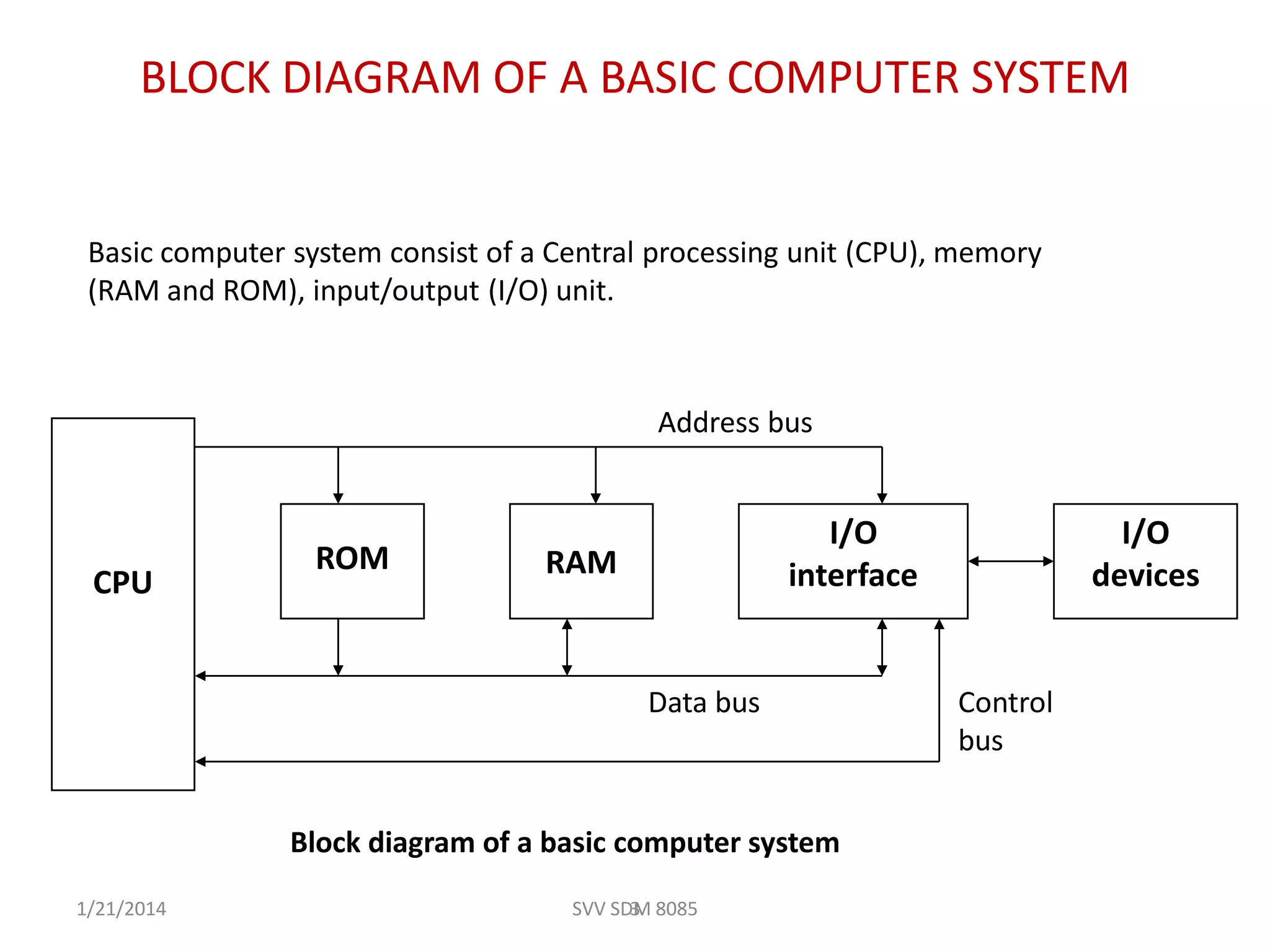
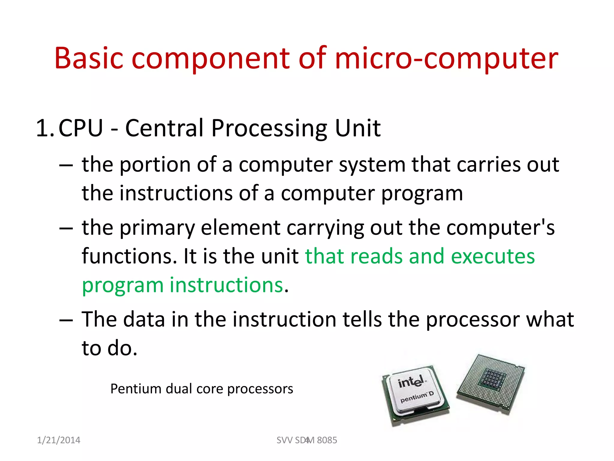
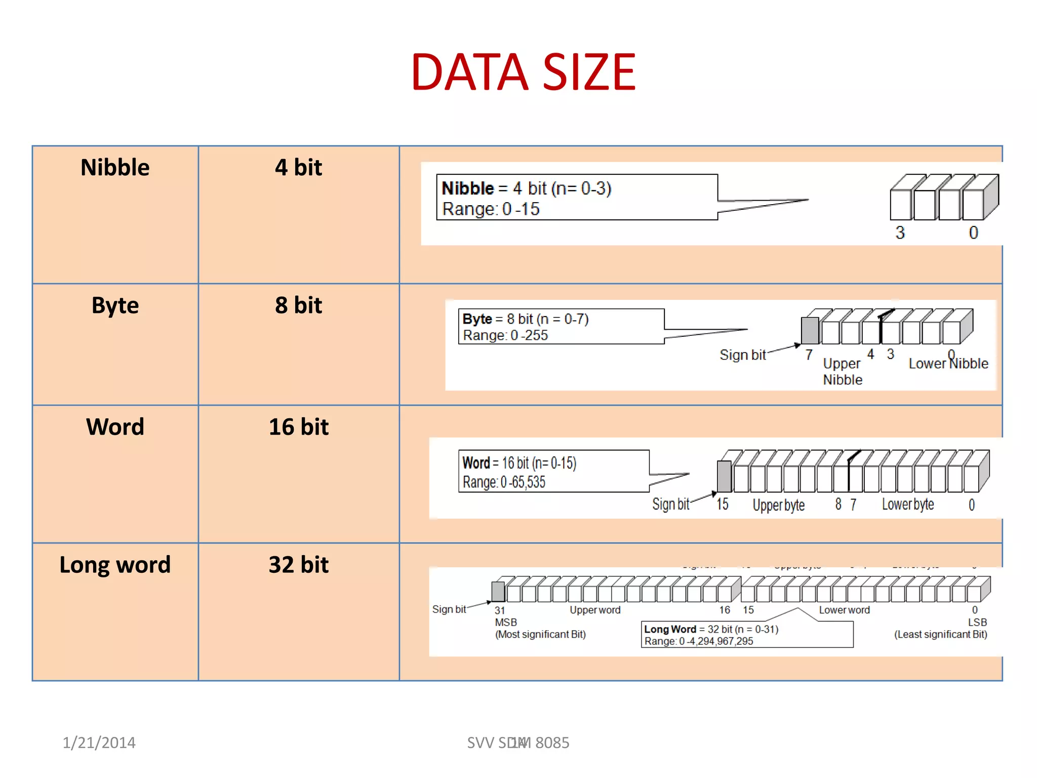
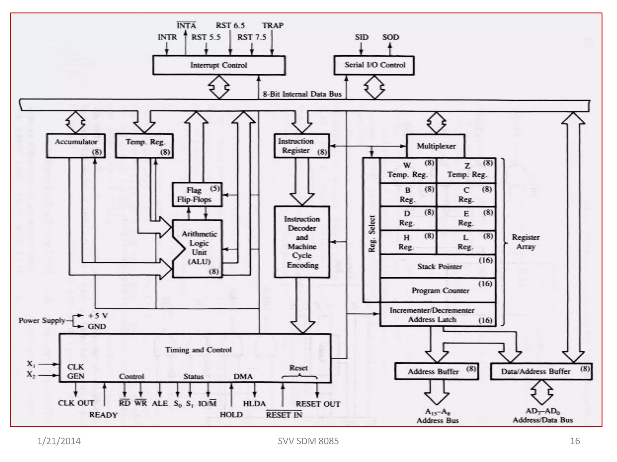
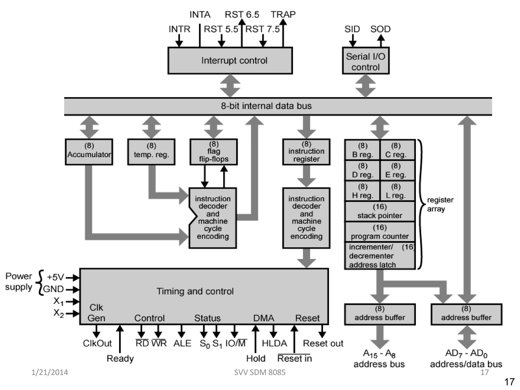
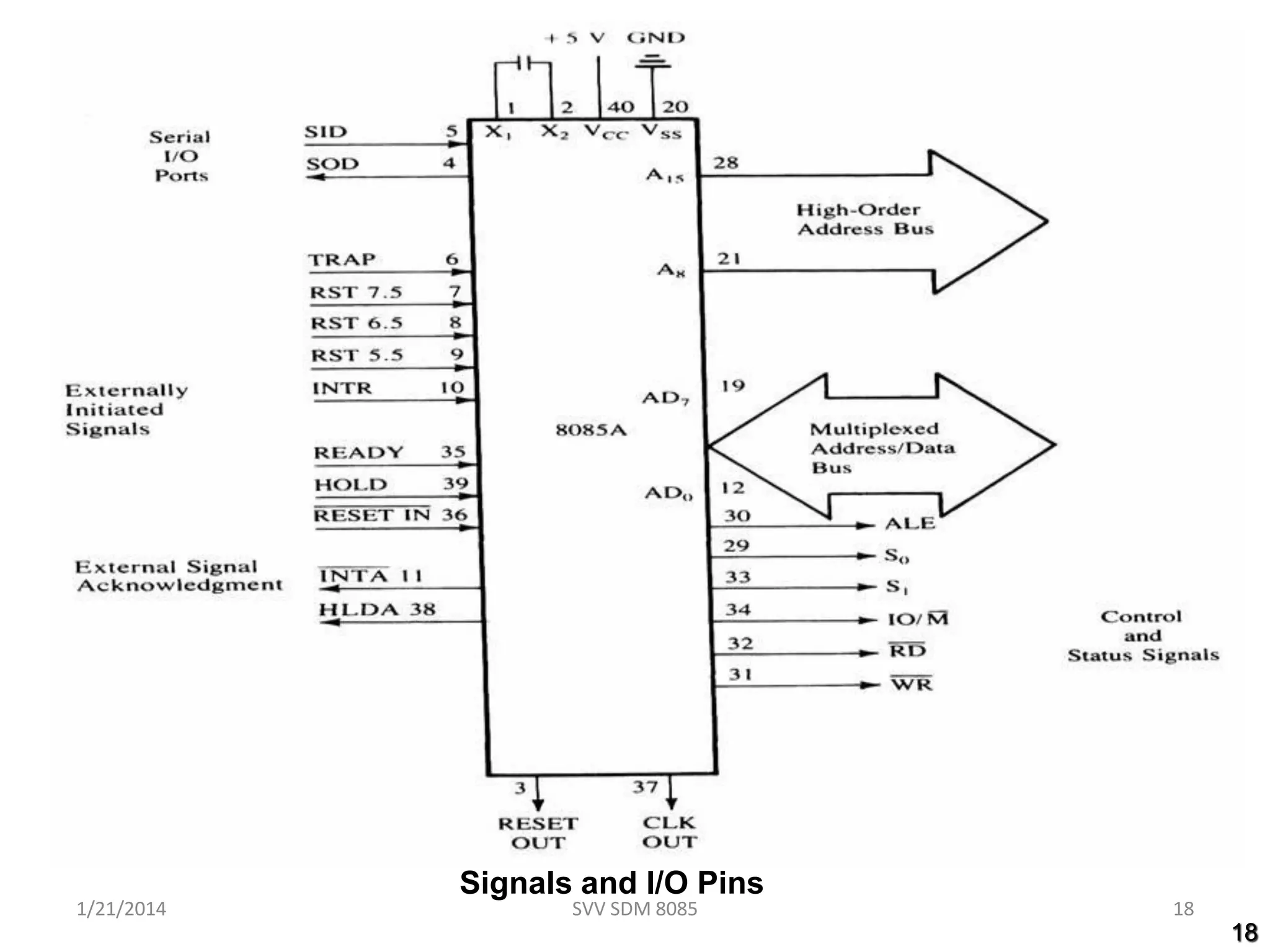
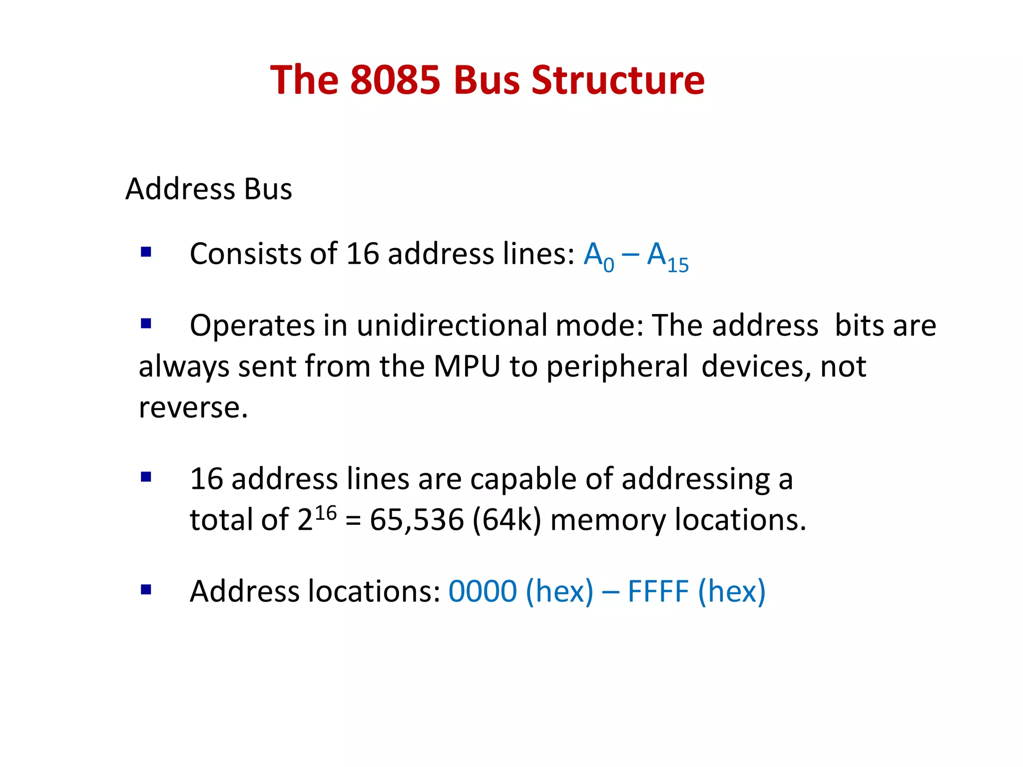
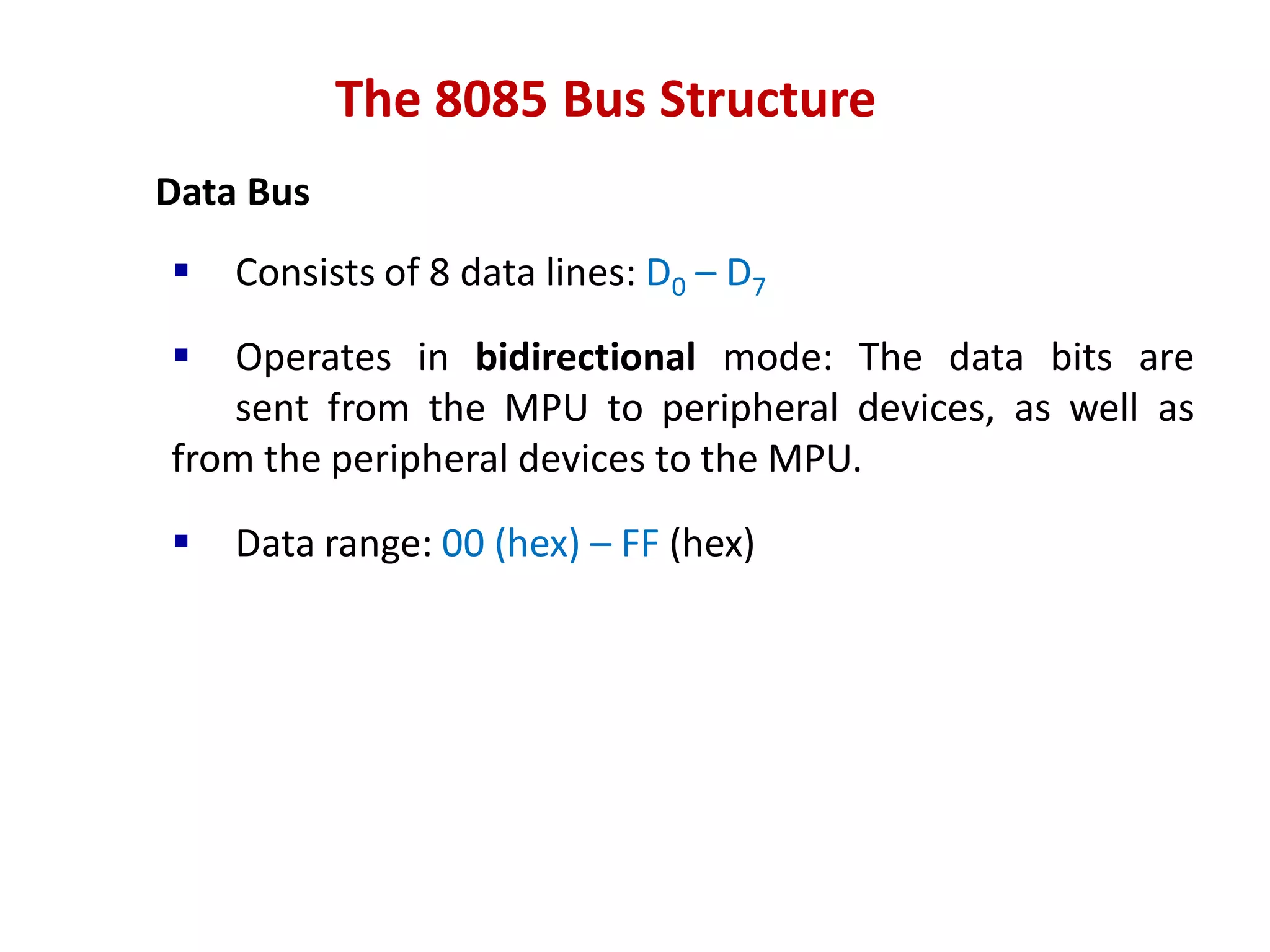
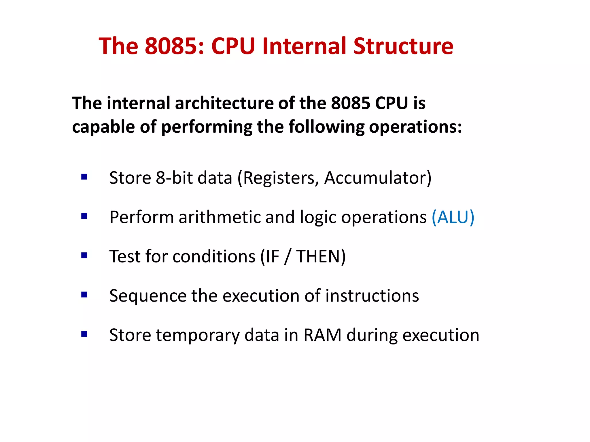
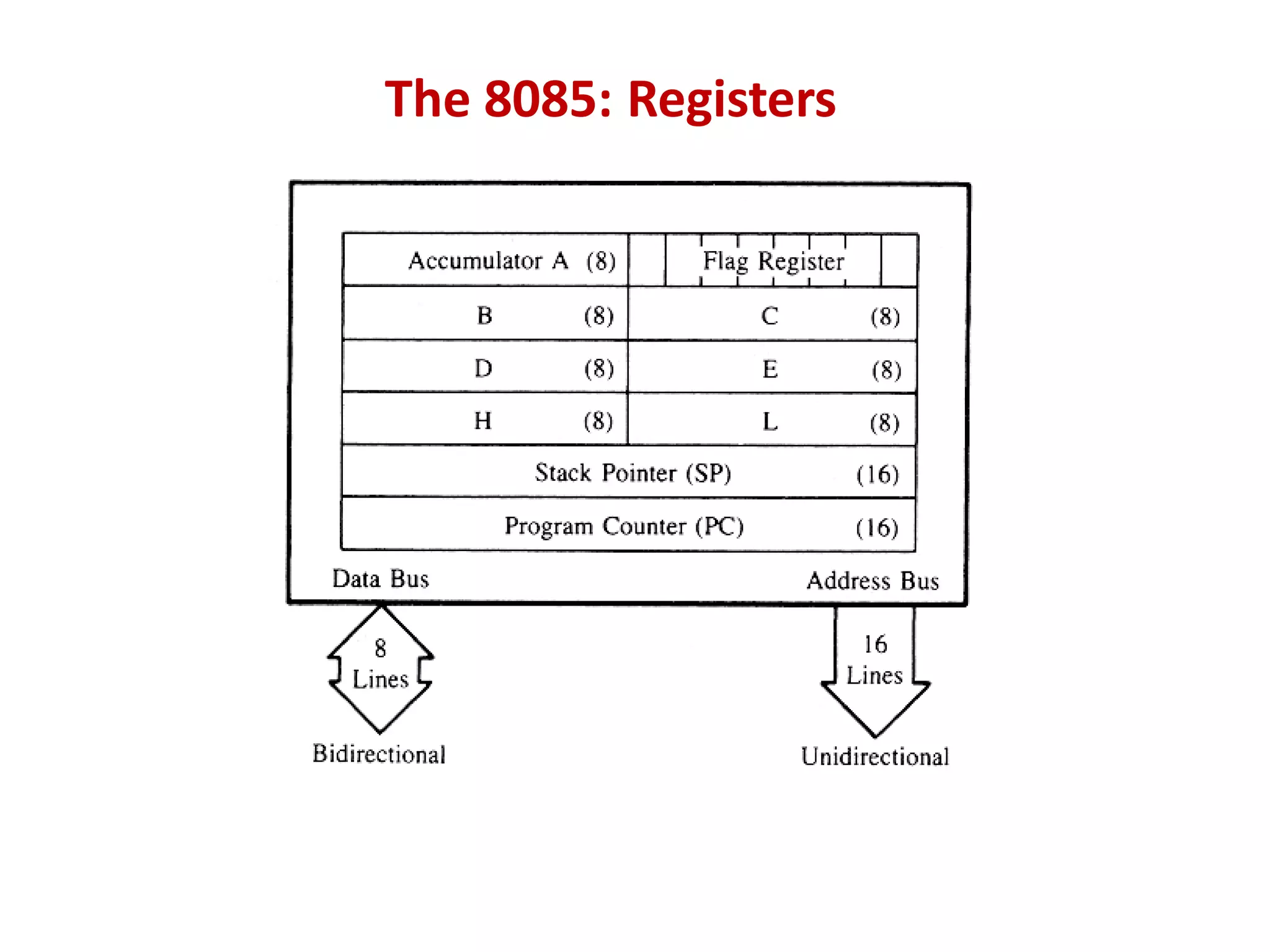
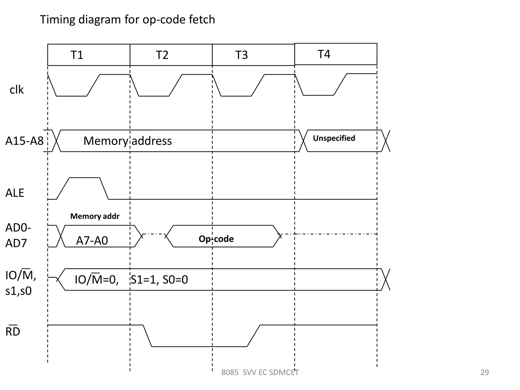
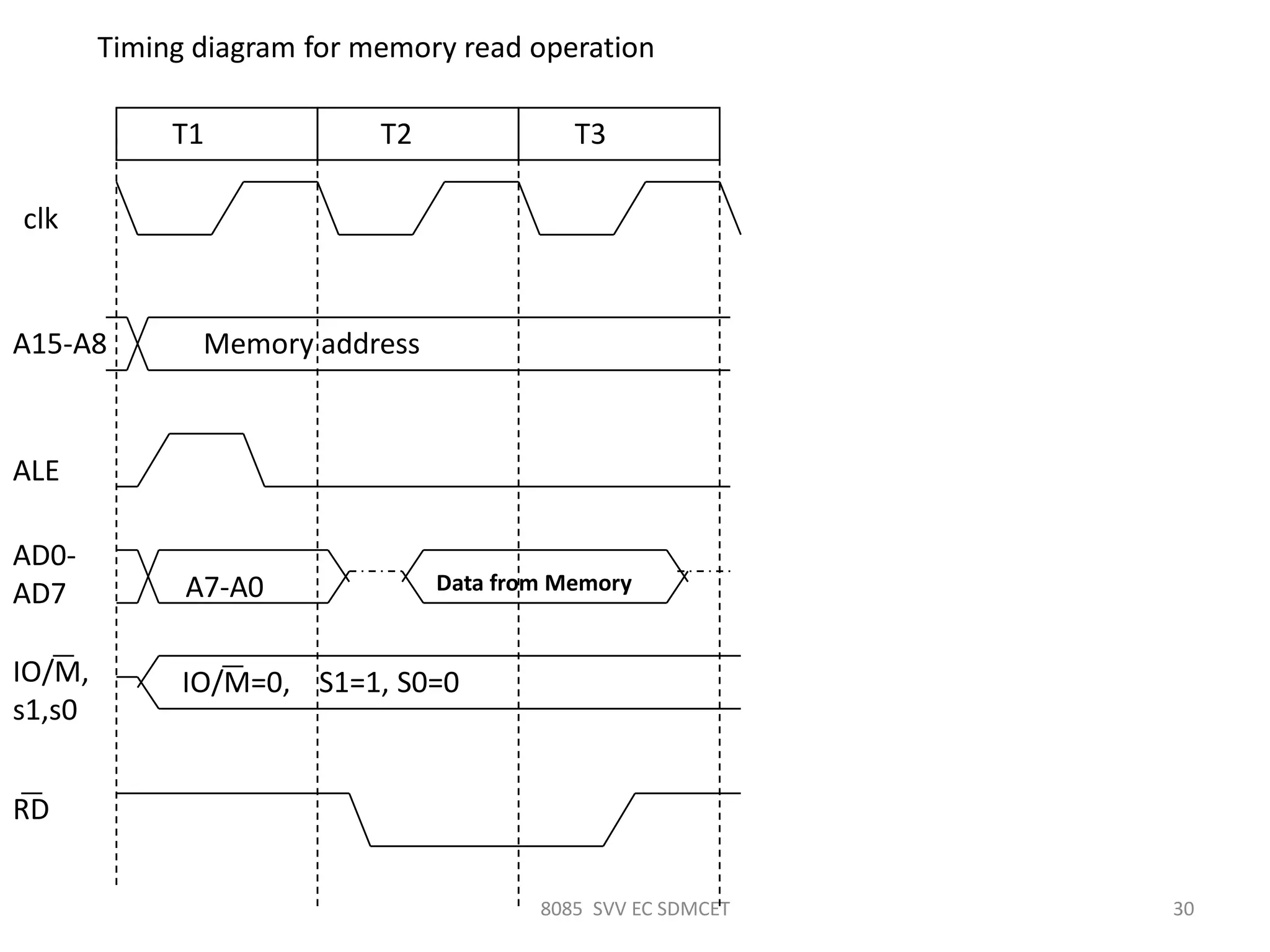
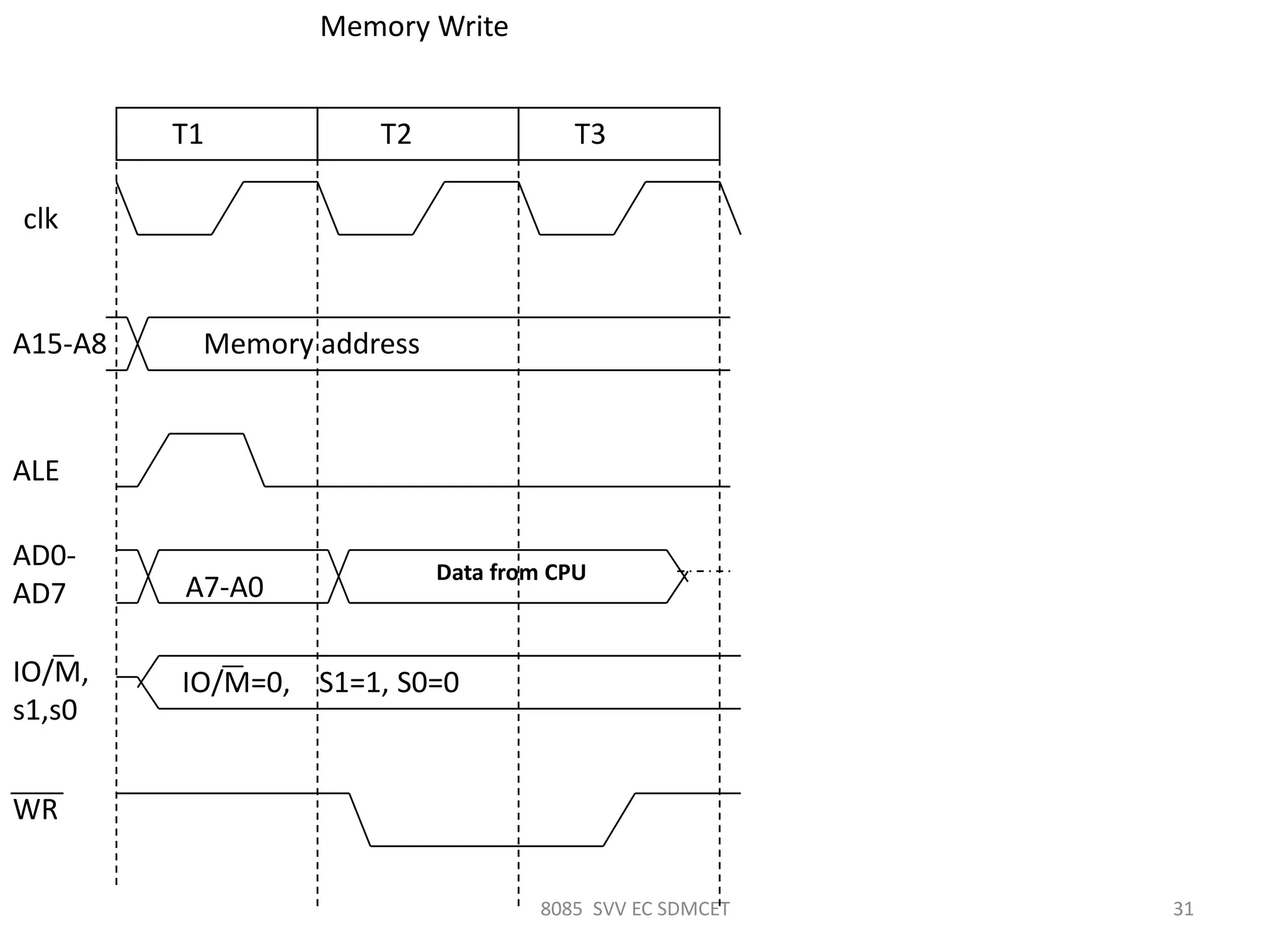
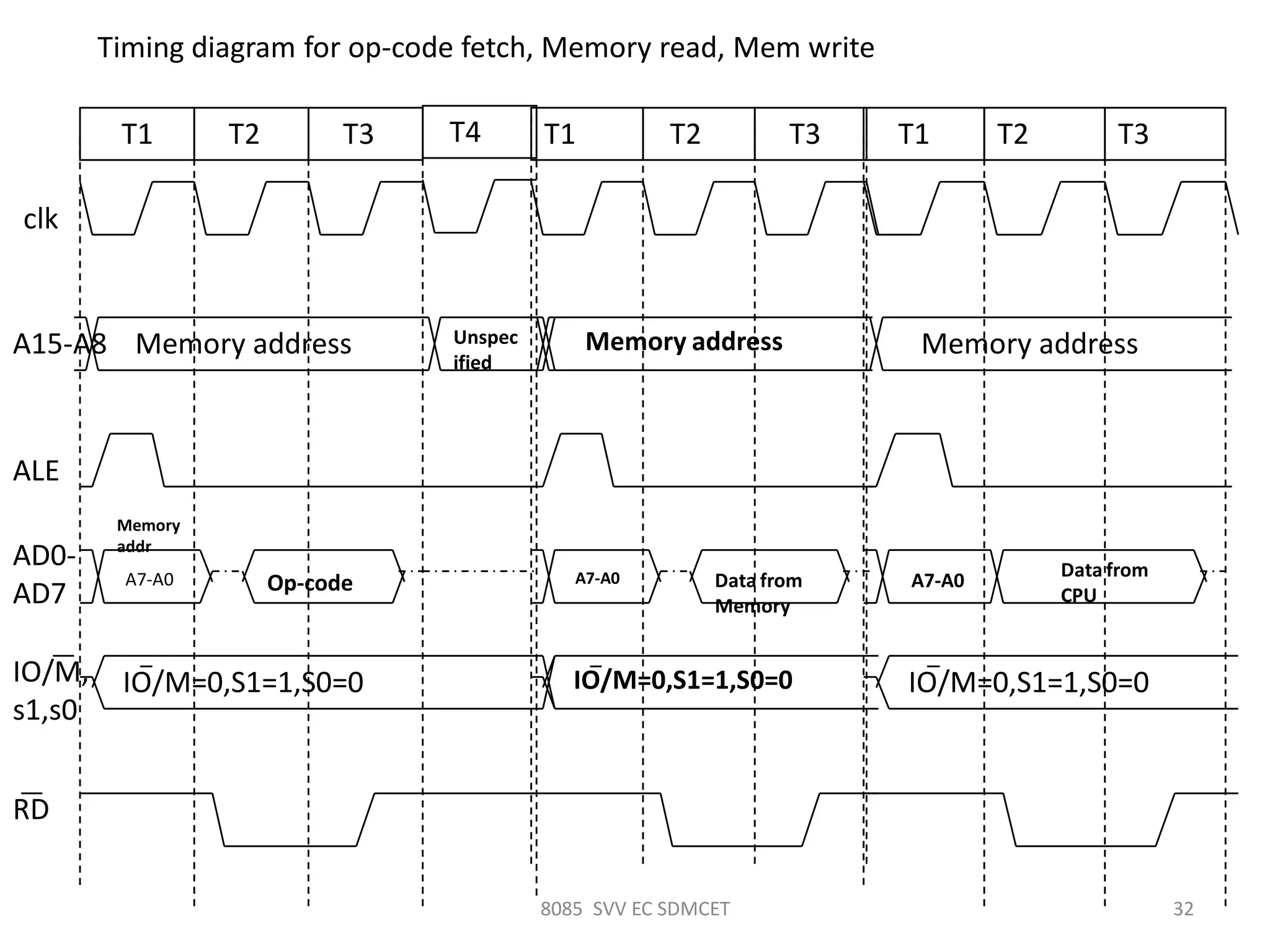
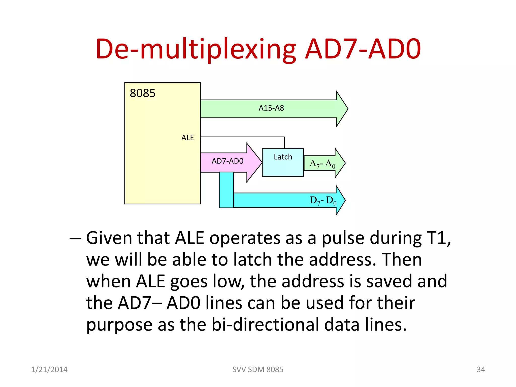
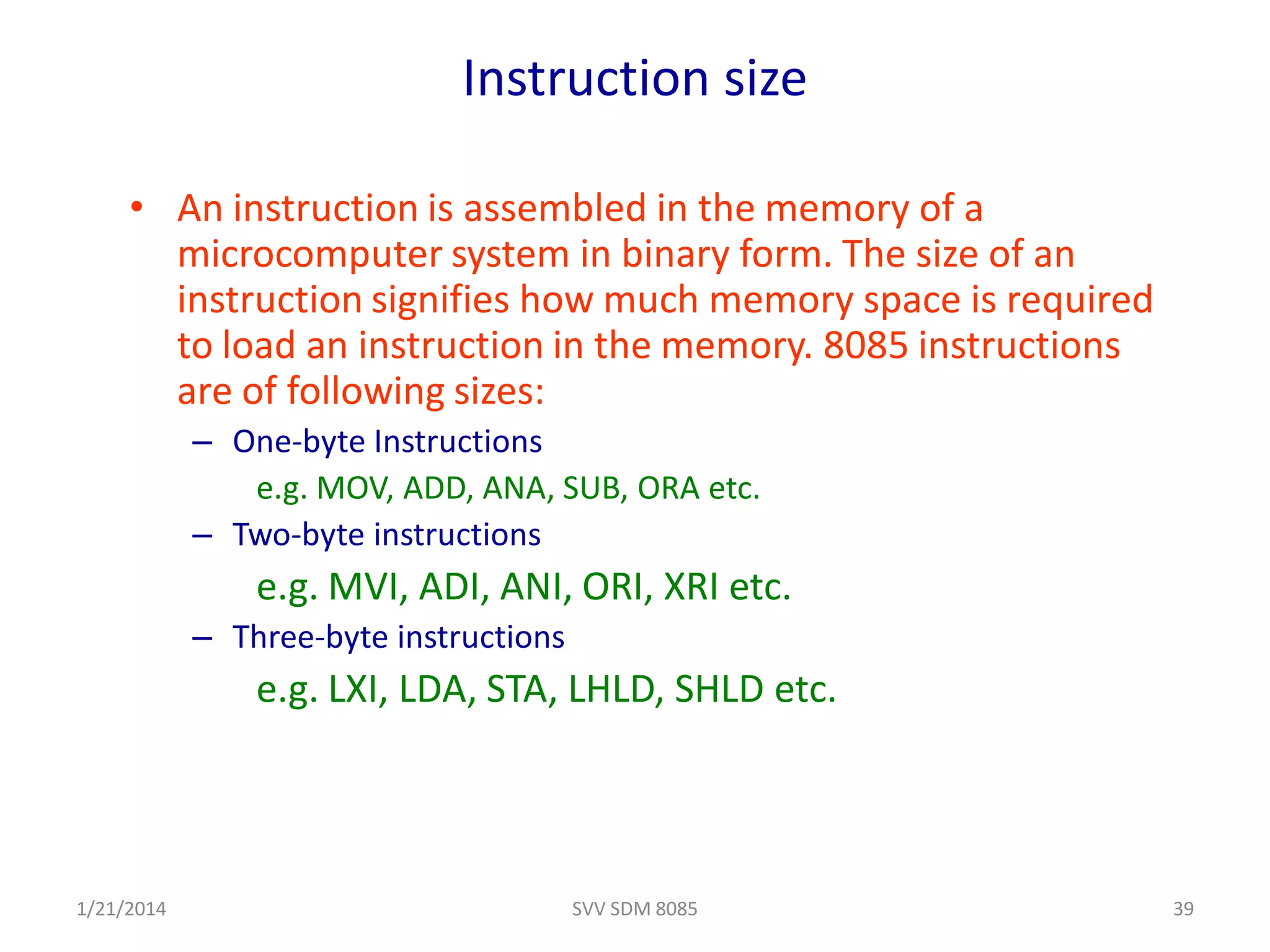
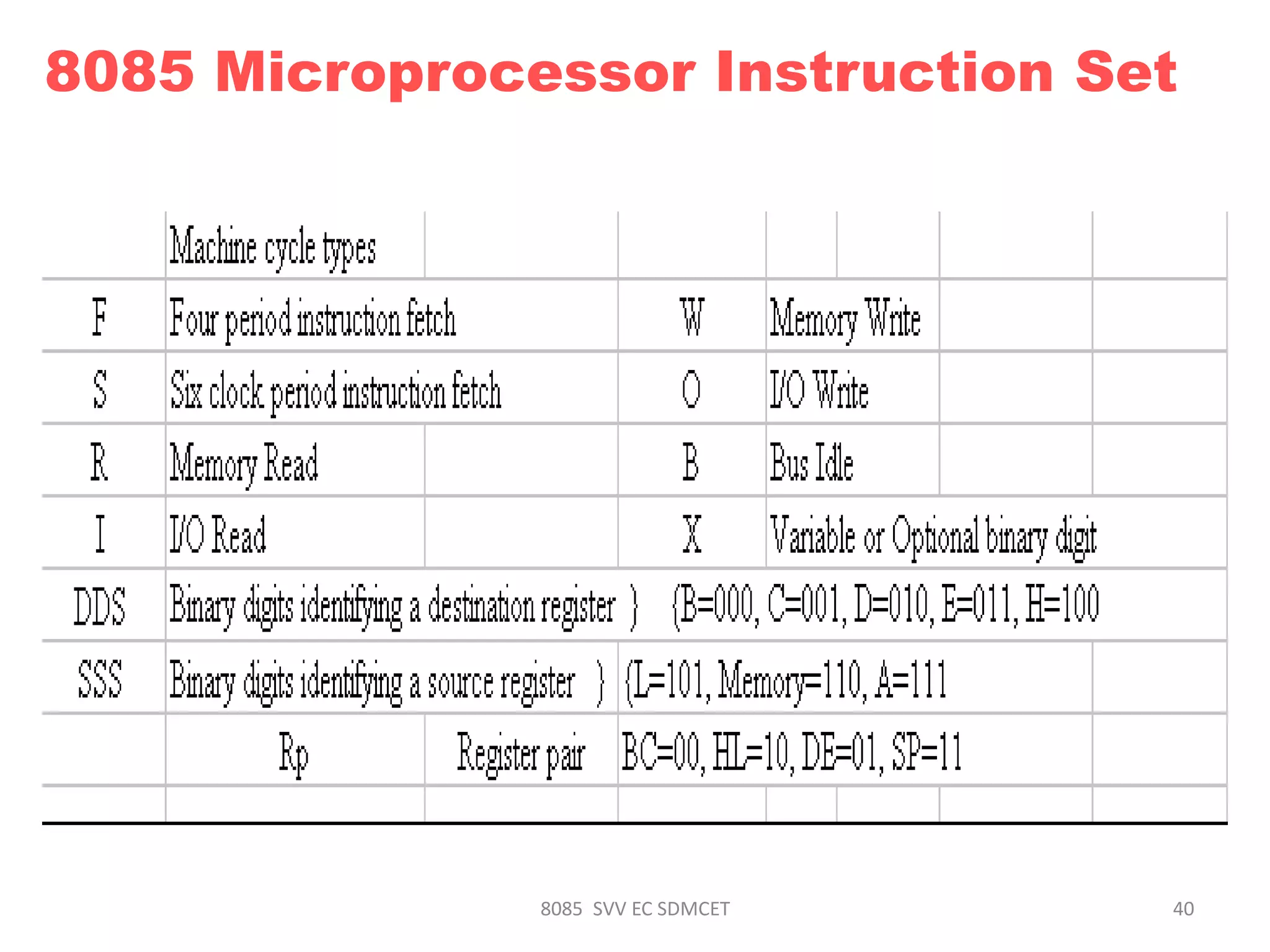
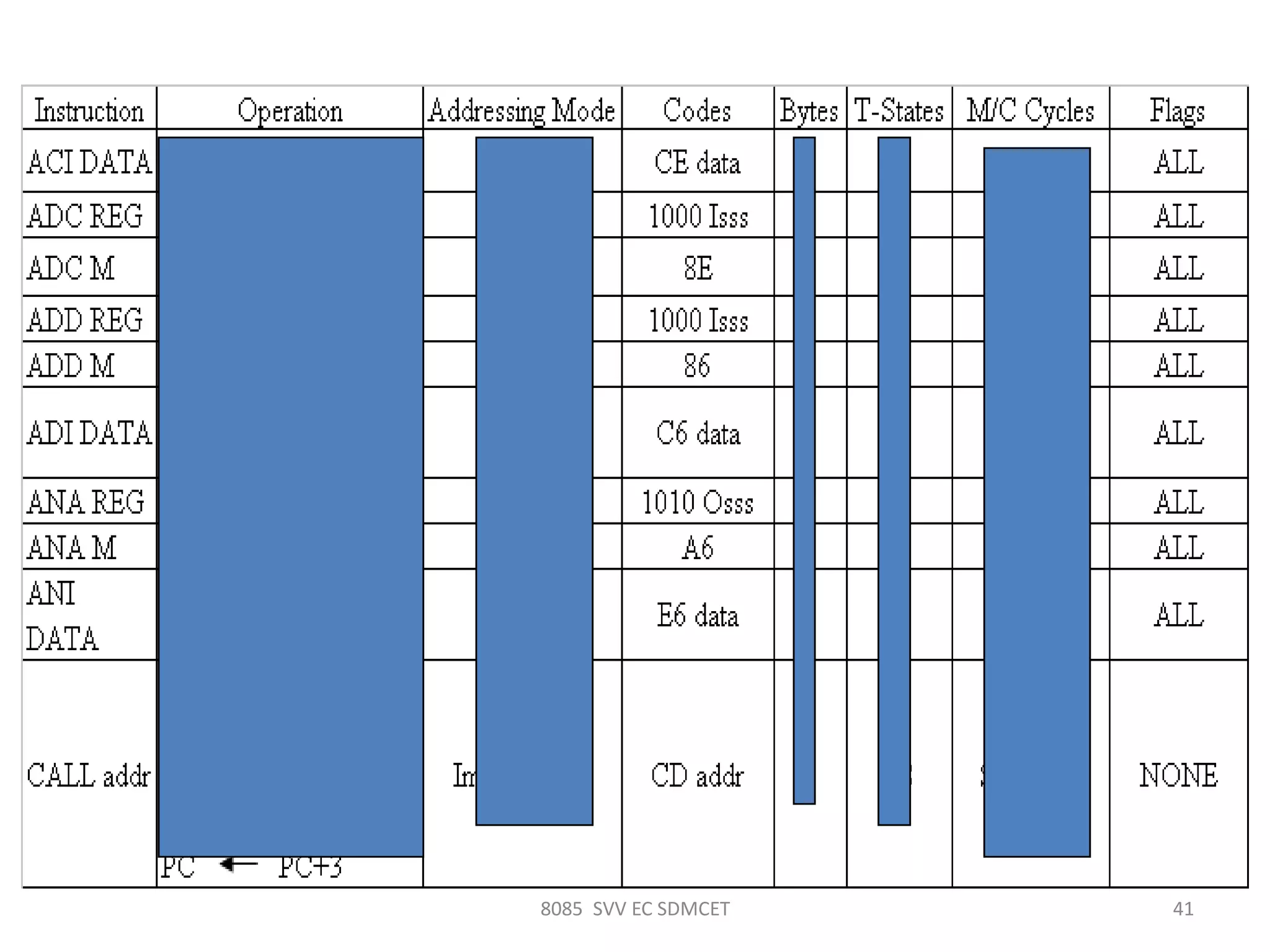
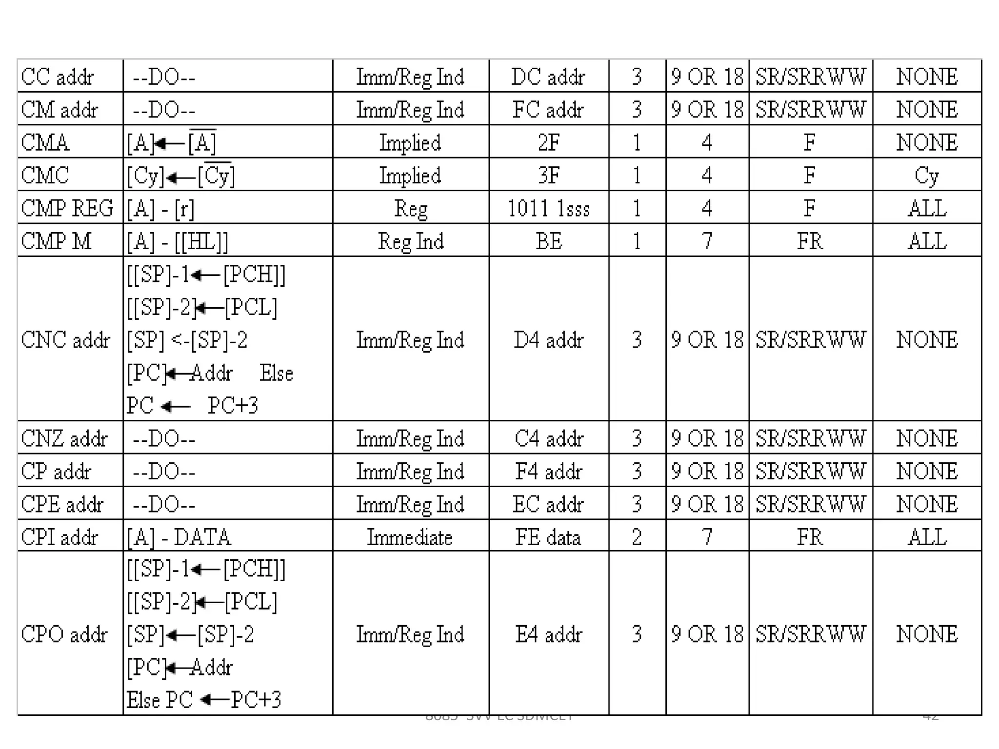
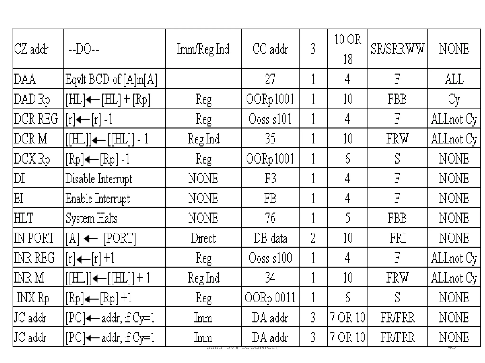
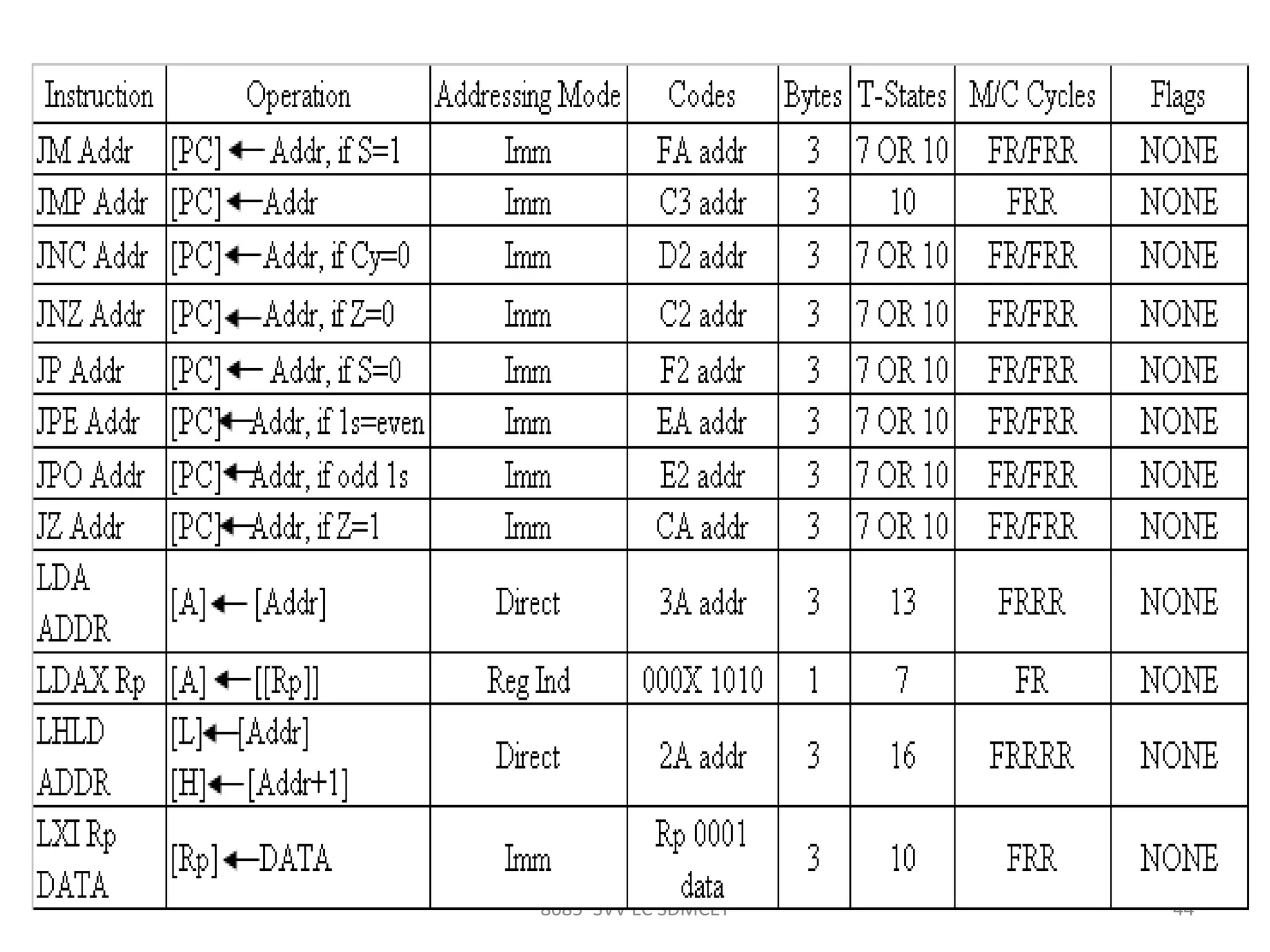
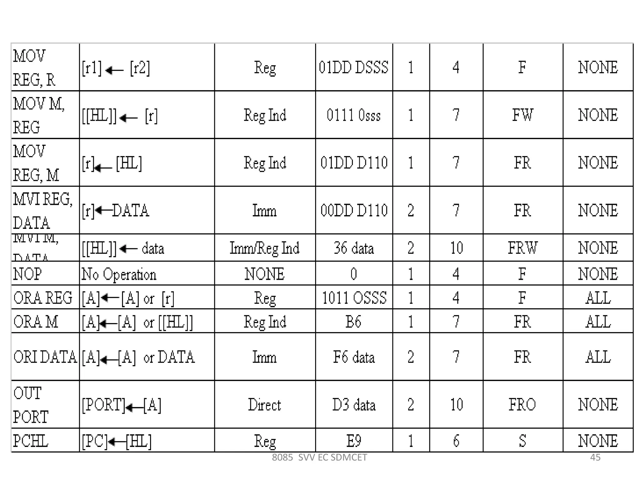
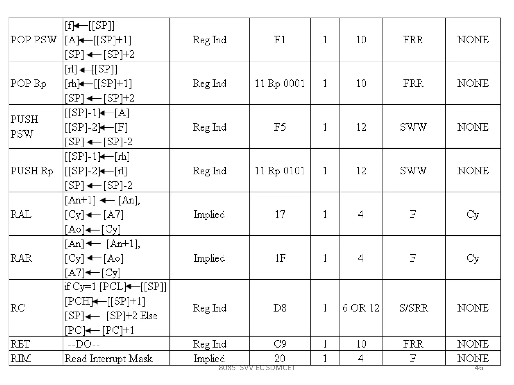
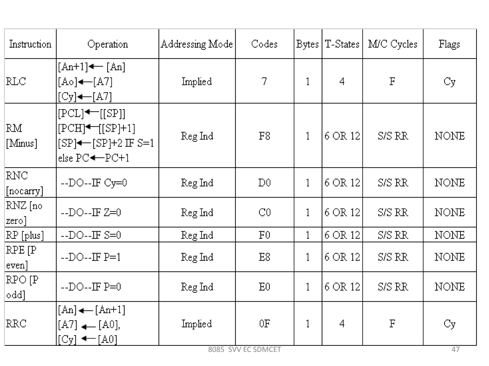
Introduction to 8085
Mr. S. V. Viraktamath
Faculty, Dept. of E&CE,
SDMCET, Dharwad.
DIAGRAM OF A COMPUTER SYSTEM
A computer is a programmable machine that receives input, stores and manipulates
data//information, and provides output in a useful format.
2
Diagram of A Computer System1/21/2014 SVV SDM 8085
BLOCK DIAGRAM OF A BASIC COMPUTER SYSTEM
ROM RAM
I/O
interface
I/O
devicesCPU
3
Basic computer system consist of a Central processing unit (CPU), memory
(RAM and ROM), input/output (I/O) unit.
Block diagram of a basic computer system
Address bus
Data bus Control
bus
1/21/2014 SVV SDM 8085
Basic component of micro-computer
1.CPU - Central Processing Unit
– the portion of a computer system that carries out
the instructions of a computer program
– the primary element carrying out the computer's
functions. It is the unit that reads and executes
program instructions.
– The data in the instruction tells the processor what
to do.
4
Pentium dual core processors
1/21/2014 SVV SDM 8085
2. Memory
– physical devices used to store data or programs (sequences
of instructions) on a temporary or permanent basis for use
in an electronic digital computer.
– Computer main memory comes in two principal varieties:
random-access memory (RAM) and read-only memory
(ROM).
– RAM can be read and written to anytime the CPU
commands it, but ROM is pre-loaded with data and
software that never changes, so the CPU can only read
from it.
51/21/2014 SVV SDM 8085
– ROM is typically used to store the computer's initial start-
up instructions.
– In general, the contents of RAM are erased when the
power to the computer is turned off, but ROM retains its
data indefinitely.
– In a PC, the ROM contains a specialized program called the
BIOS that orchestrates loading the computer's operating
system from the hard disk drive into RAM whenever the
computer is turned on or reset.
1/21/2014 SVV SDM 8085 6
Memory Classification
1/21/2014 SVV SDM 8085 7
3. I/O Unit
– Input/output (I/O), refers to the communication between an
information processing system (such as a computer), and the
outside world possibly a human, or another information
processing system.
– Inputs are the signals or data received by the system, and
outputs are the signals or data sent from it
– Devices that provide input or output to the computer are called
peripherals
– On a typical personal computer, peripherals include input
devices like the keyboard and mouse, and output devices such as
the display and printer. Hard disk drives, floppy disk drives and
optical disc drives serve as both input and output devices.
Computer networking is another form of I/O.
8
1/21/2014
SVV SDM 8085
• PMOS technology – slow and awkward to interface
with TTL family
• 4 bit processor
• Instructions were executed in about 20 µs.
• Intel 4004 the first MP. 4K nibbles address space.
• Intel 8008- can manipulate a whole byte.
• 16Kbytes address space
• 50,000 operations/second.
Early microprocessors
1/21/2014 9SVV SDM 8085
N-channel MOSFET
• 1970.
• Faster than P-MOS.
• Work with +ve supply; easy to interface with TTL.
• 1973 Intel 8080 MP.
• 500,000 operations/second.
• 64K bytes memory.
• Upward software compatible with 8008.
• Other brands are MC6800, Fairchild’s F-8 etc.
1/21/2014 10SVV SDM 8085
Modern MP
• 8, 16, 32, 64 bits are available.
• Intel 8085, Motorola 6800 – 8 bit word 16 bit
address.
• Intel 8088, 8086, Motorola 68000 – 16 bits word, 20
bits address.
• 80186 – never used.
• 286 – real mode and protected mode; 16MB
memory
• 386 – paging, 4GB memory, 32 bits word
• 486 – math coprocessor, L1 cache
1/21/2014 11SVV SDM 8085
Modern MP
• Pentium
– 64 bits i/o off the chip but process 32bits word, exception floating
point processed 64 bits, cache doubled, instruction pipelining.
• Pentium Pro
– L2 cache, Improved pipelining
• Pentium MMX
– Multi-Media extensions, 57 new inter instruc mostly used for
multimedia programming
• Pentium II, III, IV
– Pentium pro with MMX tech, increased L2 cache, full 64 bit operation
• RISC
– Reduced instruction set processor, uniform length instruc, faster in
operation, cannot perform may different thing as CISC.
1/21/2014 12SVV SDM 8085
Evolution of Microprocessor
131/21/2014 SVV SDM 8085
DATA SIZE
Nibble 4 bit
Byte 8 bit
Word 16 bit
Long word 32 bit
141/21/2014 SVV SDM 8085
Architecture of 8085
1/21/2014 SVV SDM 8085 15
SVV SDM 8085 161/21/2014
17
Intel 8085 CPU Block Diagram
1/21/2014 17SVV SDM 8085
18
Signals and I/O Pins
1/21/2014 18SVV SDM 8085
The 8085 Bus Structure
Address Bus
 Consists of 16 address lines: A0 – A15
ď‚§ Operates in unidirectional mode: The address bits are
always sent from the MPU to peripheral devices, not
reverse.
ď‚§ 16 address lines are capable of addressing a
total of 216 = 65,536 (64k) memory locations.
 Address locations: 0000 (hex) – FFFF (hex)
The 8085 Bus Structure
Data Bus
 Consists of 8 data lines: D0 – D7
ď‚§ Operates in bidirectional mode: The data bits are
sent from the MPU to peripheral devices, as well as
from the peripheral devices to the MPU.
 Data range: 00 (hex) – FF (hex)
The 8085: CPU Internal Structure
The internal architecture of the 8085 CPU is
capable of performing the following operations:
ď‚§ Store 8-bit data (Registers, Accumulator)
ď‚§ Perform arithmetic and logic operations (ALU)
ď‚§ Test for conditions (IF / THEN)
ď‚§ Sequence the execution of instructions
ď‚§ Store temporary data in RAM during execution
The 8085: Registers
The 8085: CPU Internal Structure
Registers
ď‚§ Six general purpose 8-bit registers: B, C, D, E, H, L
ď‚§ They can also be combined as register pairs to
perform 16-bit operations: BC, DE, HL
ď‚§ Registers are programmable (data load, move, etc.)
Accumulator
ď‚§ Single 8-bit register that is part of the ALU !
 Used for arithmetic / logic operations – the result is
always stored in the accumulator.
The 8085: CPU Internal Structure
Flag Bits
ď‚§ Indicate the result of condition tests.
ď‚§ Carry, Zero, Sign, Parity, etc.
ď‚§ Conditional operations (IF / THEN) are executed
based on the condition of these flag bits.
Program Counter (PC)
ď‚§ Contains the memory address (16 bits) of the
instruction that will be executed in the next step.
Stack Pointer (SP)
SVV SDM 8085 25
The Control and Status Signals
• There are 4 main control and status signals. These are:
• ALE: Address Latch Enable. This signal is a pulse that become 1
when the AD0 – AD7 lines have an address on them. It becomes 0
after that. This signal can be used to enable a latch to save the
address bits from the AD lines.
• RD: Read. Active low.
• WR: Write. Active low.
• IO/M: This signal specifies whether the operation is a memory
operation (IO/M=0) or an I/O operation (IO/M=1).
• S1 and S0 : Status signals to specify the kind of operation being
performed .Usually un-used in small systems.
1/21/2014
SVV SDM 8085 26
Frequency Control Signals
• There are 3 important pins in the frequency control group.
– X0 and X1 are the inputs from the crystal or clock generating circuit.
• The frequency is internally divided by 2.
– So, to run the microprocessor at 3 MHz, a clock running at 6
MHz should be connected to the X0 and X1 pins.
– CLK (OUT): An output clock pin to drive the clock of the rest of the
system.
1/21/2014
27
Control and Status Signals.
28
Interrupt signals
• An interrupt is a hardware-initiated subroutine CALL.
• When interrupt pin is activated, an ISR will be called,
interrupting the program that is currently executing.
Pin Subroutine Location
TRAP 0024
RST 5.5 002C
RST 6.5 0034
RST 7.5 003C
INTR *
Note: * the address of the ISR is determined by the external hardware.
8085 SVV EC SDMCET 29
Timing diagram for op-code fetch
clk
T1 T2 T3
Memory addressA15-A8
ALE
AD0-
AD7
IO/M,
s1,s0
IO/M=0, S1=1, S0=0
A7-A0 Op-code
RD
T4
Unspecified
Memory addr
8085 SVV EC SDMCET 30
Timing diagram for memory read operation
clk
T1 T2 T3
Memory addressA15-A8
ALE
AD0-
AD7
IO/M,
s1,s0
IO/M=0, S1=1, S0=0
A7-A0 Data from Memory
RD
8085 SVV EC SDMCET 31
clk
T1 T2 T3
Memory addressA15-A8
ALE
AD0-
AD7
IO/M,
s1,s0
IO/M=0, S1=1, S0=0
A7-A0
Data from CPU
WR
Memory Write
8085 SVV EC SDMCET 32
Timing diagram for op-code fetch, Memory read, Mem write
clk
A15-A8
ALE
AD0-
AD7
IO/M,
s1,s0
RD
T1 T2 T3
Memory address
IO/M=0,S1=1,S0=0
A7-A0 Op-code
T4
Unspec
ified
Memory
addr
T1 T2 T3
Memory address
IO/M=0,S1=1,S0=0
A7-A0 Data from
Memory
T1 T2 T3
Memory address
IO/M=0,S1=1,S0=0
A7-A0
Data from
CPU
SVV SDM 8085 33
De-multiplexing AD7-AD0
– From the above description, it becomes obvious that the AD7–
AD0 lines are serving a dual purpose and that they need to be
demultiplexed to get all the information.
– The high order bits of the address remain on the bus for three
clock periods. However, the low order bits remain for only one
clock period and they would be lost if they are not saved
externally. Also, notice that the low order bits of the address
disappear when they are needed most.
– To make sure we have the entire address for the full three
clock cycles, we will use an external latch to save the value of
AD7– AD0 when it is carrying the address bits. We use the ALE
signal to enable this latch.
1/21/2014
SVV SDM 8085 34
De-multiplexing AD7-AD0
– Given that ALE operates as a pulse during T1,
we will be able to latch the address. Then
when ALE goes low, the address is saved and
the AD7– AD0 lines can be used for their
purpose as the bi-directional data lines.
A15-A8
LatchAD7-AD0
D7- D0
A7- A0
8085
ALE
1/21/2014
SVV SDM 8085 35
Cycles and States
• From the above discussion, we can define terms that will become
handy later on:
– T- State: One subdivision of an operation. A T-state lasts for one
clock period.
• An instruction’s execution length is usually measured in a
number of T-states. (clock cycles).
– Machine Cycle: The time required to complete one operation of
accessing memory, I/O, or acknowledging an external request.
• This cycle may consist of 3 to 6 T-states.
– Instruction Cycle: The time required to complete the execution
of an instruction.
• In the 8085, an instruction cycle may consist of 1 to 6
machine cycles.
1/21/2014
SVV SDM 8085 36
Generating Control Signals
• The 8085 generates a single RD signal. However, the signal needs to be
used with both memory and I/O. So, it must be combined with the IO/M
signal to generate different control signals for the memory and I/O.
– Keeping in mind the operation of the IO/M signal we can use the
following circuitry to generate the right set of signals:
1/21/2014
Addressing Modes
• 8085 instructions can be classified in
following addressing modes
– Register Addressing mode
• Instructions which have their operands in registers only
e.g. MOV, ADD, SUB, ANA, ORA, XRA etc.
– Immediate Addressing mode
• Instructions in which operand immediately follows the
op-code e.g. MVI, LXI, ADI, SUI, ANI, ORI etc.
– Direct Addressing mode
• Instructions have their operands in memory and the
16-bit memory address is specified in the instruction e.g.
LDA, STA, LHLD, SHLD etc.
1/21/2014 37SVV SDM 8085
Addressing Modes Contd..
– Register Indirect Addressing mode
• Instructions have their operand in memory and the 16-bit
memory address is specified in a register pair e.g. LDAX,
STAX, PUSH, POP etc.
– Implicit Addressing mode
• These instruction have their operand implied in the op-
code itself e.g. CMA, CMC, STC etc.
1/21/2014 38SVV SDM 8085
Instruction size
• An instruction is assembled in the memory of a
microcomputer system in binary form. The size of an
instruction signifies how much memory space is required
to load an instruction in the memory. 8085 instructions
are of following sizes:
– One-byte Instructions
e.g. MOV, ADD, ANA, SUB, ORA etc.
– Two-byte instructions
e.g. MVI, ADI, ANI, ORI, XRI etc.
– Three-byte instructions
e.g. LXI, LDA, STA, LHLD, SHLD etc.
1/21/2014 39SVV SDM 8085
8085 SVV EC SDMCET 40
8085 Microprocessor Instruction Set
8085 SVV EC SDMCET 41
8085 SVV EC SDMCET 42
8085 SVV EC SDMCET 43
8085 SVV EC SDMCET 44
8085 SVV EC SDMCET 45
8085 SVV EC SDMCET 46
8085 SVV EC SDMCET 47
8085 SVV EC SDMCET 48

Introduction to 8085svv

  • 1.
    Introduction to 8085 Mr.S. V. Viraktamath Faculty, Dept. of E&CE, SDMCET, Dharwad.
  • 2.
    DIAGRAM OF ACOMPUTER SYSTEM A computer is a programmable machine that receives input, stores and manipulates data//information, and provides output in a useful format. 2 Diagram of A Computer System1/21/2014 SVV SDM 8085
  • 3.
    BLOCK DIAGRAM OFA BASIC COMPUTER SYSTEM ROM RAM I/O interface I/O devicesCPU 3 Basic computer system consist of a Central processing unit (CPU), memory (RAM and ROM), input/output (I/O) unit. Block diagram of a basic computer system Address bus Data bus Control bus 1/21/2014 SVV SDM 8085
  • 4.
    Basic component ofmicro-computer 1.CPU - Central Processing Unit – the portion of a computer system that carries out the instructions of a computer program – the primary element carrying out the computer's functions. It is the unit that reads and executes program instructions. – The data in the instruction tells the processor what to do. 4 Pentium dual core processors 1/21/2014 SVV SDM 8085
  • 5.
    2. Memory – physicaldevices used to store data or programs (sequences of instructions) on a temporary or permanent basis for use in an electronic digital computer. – Computer main memory comes in two principal varieties: random-access memory (RAM) and read-only memory (ROM). – RAM can be read and written to anytime the CPU commands it, but ROM is pre-loaded with data and software that never changes, so the CPU can only read from it. 51/21/2014 SVV SDM 8085
  • 6.
    – ROM istypically used to store the computer's initial start- up instructions. – In general, the contents of RAM are erased when the power to the computer is turned off, but ROM retains its data indefinitely. – In a PC, the ROM contains a specialized program called the BIOS that orchestrates loading the computer's operating system from the hard disk drive into RAM whenever the computer is turned on or reset. 1/21/2014 SVV SDM 8085 6
  • 7.
  • 8.
    3. I/O Unit –Input/output (I/O), refers to the communication between an information processing system (such as a computer), and the outside world possibly a human, or another information processing system. – Inputs are the signals or data received by the system, and outputs are the signals or data sent from it – Devices that provide input or output to the computer are called peripherals – On a typical personal computer, peripherals include input devices like the keyboard and mouse, and output devices such as the display and printer. Hard disk drives, floppy disk drives and optical disc drives serve as both input and output devices. Computer networking is another form of I/O. 8 1/21/2014 SVV SDM 8085
  • 9.
    • PMOS technology– slow and awkward to interface with TTL family • 4 bit processor • Instructions were executed in about 20 µs. • Intel 4004 the first MP. 4K nibbles address space. • Intel 8008- can manipulate a whole byte. • 16Kbytes address space • 50,000 operations/second. Early microprocessors 1/21/2014 9SVV SDM 8085
  • 10.
    N-channel MOSFET • 1970. •Faster than P-MOS. • Work with +ve supply; easy to interface with TTL. • 1973 Intel 8080 MP. • 500,000 operations/second. • 64K bytes memory. • Upward software compatible with 8008. • Other brands are MC6800, Fairchild’s F-8 etc. 1/21/2014 10SVV SDM 8085
  • 11.
    Modern MP • 8,16, 32, 64 bits are available. • Intel 8085, Motorola 6800 – 8 bit word 16 bit address. • Intel 8088, 8086, Motorola 68000 – 16 bits word, 20 bits address. • 80186 – never used. • 286 – real mode and protected mode; 16MB memory • 386 – paging, 4GB memory, 32 bits word • 486 – math coprocessor, L1 cache 1/21/2014 11SVV SDM 8085
  • 12.
    Modern MP • Pentium –64 bits i/o off the chip but process 32bits word, exception floating point processed 64 bits, cache doubled, instruction pipelining. • Pentium Pro – L2 cache, Improved pipelining • Pentium MMX – Multi-Media extensions, 57 new inter instruc mostly used for multimedia programming • Pentium II, III, IV – Pentium pro with MMX tech, increased L2 cache, full 64 bit operation • RISC – Reduced instruction set processor, uniform length instruc, faster in operation, cannot perform may different thing as CISC. 1/21/2014 12SVV SDM 8085
  • 13.
  • 14.
    DATA SIZE Nibble 4bit Byte 8 bit Word 16 bit Long word 32 bit 141/21/2014 SVV SDM 8085
  • 15.
  • 16.
    SVV SDM 8085161/21/2014
  • 17.
    17 Intel 8085 CPUBlock Diagram 1/21/2014 17SVV SDM 8085
  • 18.
    18 Signals and I/OPins 1/21/2014 18SVV SDM 8085
  • 19.
    The 8085 BusStructure Address Bus  Consists of 16 address lines: A0 – A15  Operates in unidirectional mode: The address bits are always sent from the MPU to peripheral devices, not reverse.  16 address lines are capable of addressing a total of 216 = 65,536 (64k) memory locations.  Address locations: 0000 (hex) – FFFF (hex)
  • 20.
    The 8085 BusStructure Data Bus  Consists of 8 data lines: D0 – D7  Operates in bidirectional mode: The data bits are sent from the MPU to peripheral devices, as well as from the peripheral devices to the MPU.  Data range: 00 (hex) – FF (hex)
  • 21.
    The 8085: CPUInternal Structure The internal architecture of the 8085 CPU is capable of performing the following operations: ď‚§ Store 8-bit data (Registers, Accumulator) ď‚§ Perform arithmetic and logic operations (ALU) ď‚§ Test for conditions (IF / THEN) ď‚§ Sequence the execution of instructions ď‚§ Store temporary data in RAM during execution
  • 22.
  • 23.
    The 8085: CPUInternal Structure Registers  Six general purpose 8-bit registers: B, C, D, E, H, L  They can also be combined as register pairs to perform 16-bit operations: BC, DE, HL  Registers are programmable (data load, move, etc.) Accumulator  Single 8-bit register that is part of the ALU !  Used for arithmetic / logic operations – the result is always stored in the accumulator.
  • 24.
    The 8085: CPUInternal Structure Flag Bits ď‚§ Indicate the result of condition tests. ď‚§ Carry, Zero, Sign, Parity, etc. ď‚§ Conditional operations (IF / THEN) are executed based on the condition of these flag bits. Program Counter (PC) ď‚§ Contains the memory address (16 bits) of the instruction that will be executed in the next step. Stack Pointer (SP)
  • 25.
    SVV SDM 808525 The Control and Status Signals • There are 4 main control and status signals. These are: • ALE: Address Latch Enable. This signal is a pulse that become 1 when the AD0 – AD7 lines have an address on them. It becomes 0 after that. This signal can be used to enable a latch to save the address bits from the AD lines. • RD: Read. Active low. • WR: Write. Active low. • IO/M: This signal specifies whether the operation is a memory operation (IO/M=0) or an I/O operation (IO/M=1). • S1 and S0 : Status signals to specify the kind of operation being performed .Usually un-used in small systems. 1/21/2014
  • 26.
    SVV SDM 808526 Frequency Control Signals • There are 3 important pins in the frequency control group. – X0 and X1 are the inputs from the crystal or clock generating circuit. • The frequency is internally divided by 2. – So, to run the microprocessor at 3 MHz, a clock running at 6 MHz should be connected to the X0 and X1 pins. – CLK (OUT): An output clock pin to drive the clock of the rest of the system. 1/21/2014
  • 27.
  • 28.
    28 Interrupt signals • Aninterrupt is a hardware-initiated subroutine CALL. • When interrupt pin is activated, an ISR will be called, interrupting the program that is currently executing. Pin Subroutine Location TRAP 0024 RST 5.5 002C RST 6.5 0034 RST 7.5 003C INTR * Note: * the address of the ISR is determined by the external hardware.
  • 29.
    8085 SVV ECSDMCET 29 Timing diagram for op-code fetch clk T1 T2 T3 Memory addressA15-A8 ALE AD0- AD7 IO/M, s1,s0 IO/M=0, S1=1, S0=0 A7-A0 Op-code RD T4 Unspecified Memory addr
  • 30.
    8085 SVV ECSDMCET 30 Timing diagram for memory read operation clk T1 T2 T3 Memory addressA15-A8 ALE AD0- AD7 IO/M, s1,s0 IO/M=0, S1=1, S0=0 A7-A0 Data from Memory RD
  • 31.
    8085 SVV ECSDMCET 31 clk T1 T2 T3 Memory addressA15-A8 ALE AD0- AD7 IO/M, s1,s0 IO/M=0, S1=1, S0=0 A7-A0 Data from CPU WR Memory Write
  • 32.
    8085 SVV ECSDMCET 32 Timing diagram for op-code fetch, Memory read, Mem write clk A15-A8 ALE AD0- AD7 IO/M, s1,s0 RD T1 T2 T3 Memory address IO/M=0,S1=1,S0=0 A7-A0 Op-code T4 Unspec ified Memory addr T1 T2 T3 Memory address IO/M=0,S1=1,S0=0 A7-A0 Data from Memory T1 T2 T3 Memory address IO/M=0,S1=1,S0=0 A7-A0 Data from CPU
  • 33.
    SVV SDM 808533 De-multiplexing AD7-AD0 – From the above description, it becomes obvious that the AD7– AD0 lines are serving a dual purpose and that they need to be demultiplexed to get all the information. – The high order bits of the address remain on the bus for three clock periods. However, the low order bits remain for only one clock period and they would be lost if they are not saved externally. Also, notice that the low order bits of the address disappear when they are needed most. – To make sure we have the entire address for the full three clock cycles, we will use an external latch to save the value of AD7– AD0 when it is carrying the address bits. We use the ALE signal to enable this latch. 1/21/2014
  • 34.
    SVV SDM 808534 De-multiplexing AD7-AD0 – Given that ALE operates as a pulse during T1, we will be able to latch the address. Then when ALE goes low, the address is saved and the AD7– AD0 lines can be used for their purpose as the bi-directional data lines. A15-A8 LatchAD7-AD0 D7- D0 A7- A0 8085 ALE 1/21/2014
  • 35.
    SVV SDM 808535 Cycles and States • From the above discussion, we can define terms that will become handy later on: – T- State: One subdivision of an operation. A T-state lasts for one clock period. • An instruction’s execution length is usually measured in a number of T-states. (clock cycles). – Machine Cycle: The time required to complete one operation of accessing memory, I/O, or acknowledging an external request. • This cycle may consist of 3 to 6 T-states. – Instruction Cycle: The time required to complete the execution of an instruction. • In the 8085, an instruction cycle may consist of 1 to 6 machine cycles. 1/21/2014
  • 36.
    SVV SDM 808536 Generating Control Signals • The 8085 generates a single RD signal. However, the signal needs to be used with both memory and I/O. So, it must be combined with the IO/M signal to generate different control signals for the memory and I/O. – Keeping in mind the operation of the IO/M signal we can use the following circuitry to generate the right set of signals: 1/21/2014
  • 37.
    Addressing Modes • 8085instructions can be classified in following addressing modes – Register Addressing mode • Instructions which have their operands in registers only e.g. MOV, ADD, SUB, ANA, ORA, XRA etc. – Immediate Addressing mode • Instructions in which operand immediately follows the op-code e.g. MVI, LXI, ADI, SUI, ANI, ORI etc. – Direct Addressing mode • Instructions have their operands in memory and the 16-bit memory address is specified in the instruction e.g. LDA, STA, LHLD, SHLD etc. 1/21/2014 37SVV SDM 8085
  • 38.
    Addressing Modes Contd.. –Register Indirect Addressing mode • Instructions have their operand in memory and the 16-bit memory address is specified in a register pair e.g. LDAX, STAX, PUSH, POP etc. – Implicit Addressing mode • These instruction have their operand implied in the op- code itself e.g. CMA, CMC, STC etc. 1/21/2014 38SVV SDM 8085
  • 39.
    Instruction size • Aninstruction is assembled in the memory of a microcomputer system in binary form. The size of an instruction signifies how much memory space is required to load an instruction in the memory. 8085 instructions are of following sizes: – One-byte Instructions e.g. MOV, ADD, ANA, SUB, ORA etc. – Two-byte instructions e.g. MVI, ADI, ANI, ORI, XRI etc. – Three-byte instructions e.g. LXI, LDA, STA, LHLD, SHLD etc. 1/21/2014 39SVV SDM 8085
  • 40.
    8085 SVV ECSDMCET 40 8085 Microprocessor Instruction Set
  • 41.
    8085 SVV ECSDMCET 41
  • 42.
    8085 SVV ECSDMCET 42
  • 43.
    8085 SVV ECSDMCET 43
  • 44.
    8085 SVV ECSDMCET 44
  • 45.
    8085 SVV ECSDMCET 45
  • 46.
    8085 SVV ECSDMCET 46
  • 47.
    8085 SVV ECSDMCET 47
  • 48.
    8085 SVV ECSDMCET 48