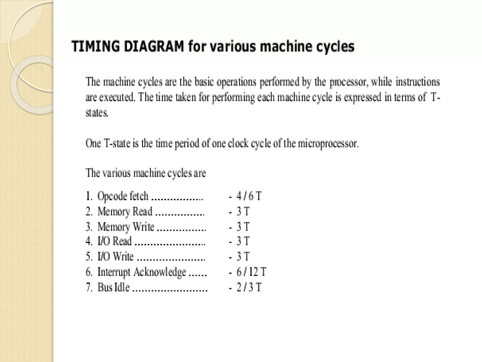
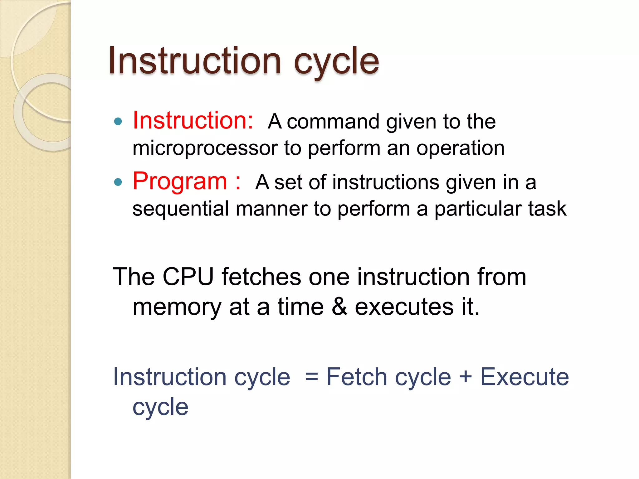
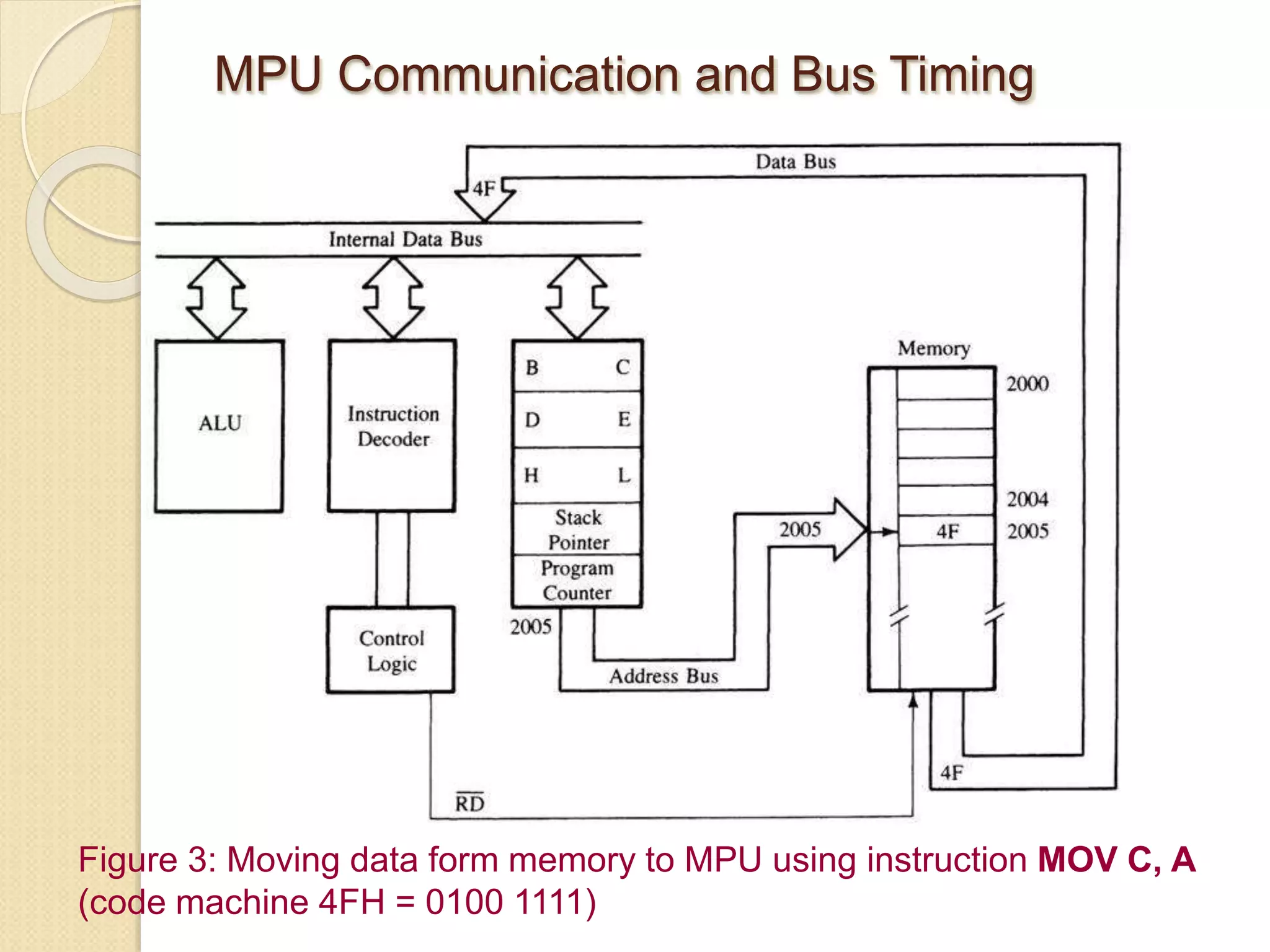
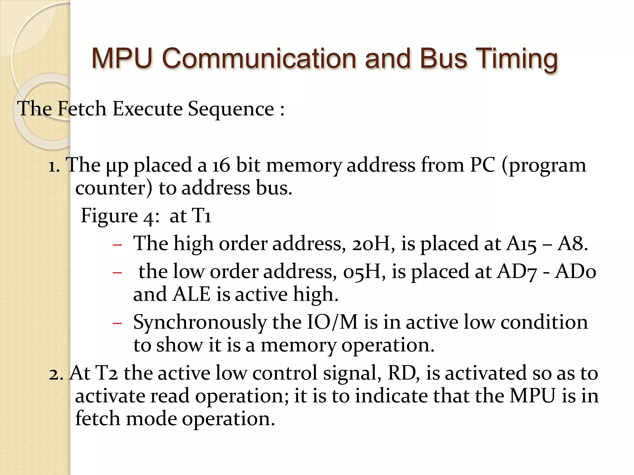
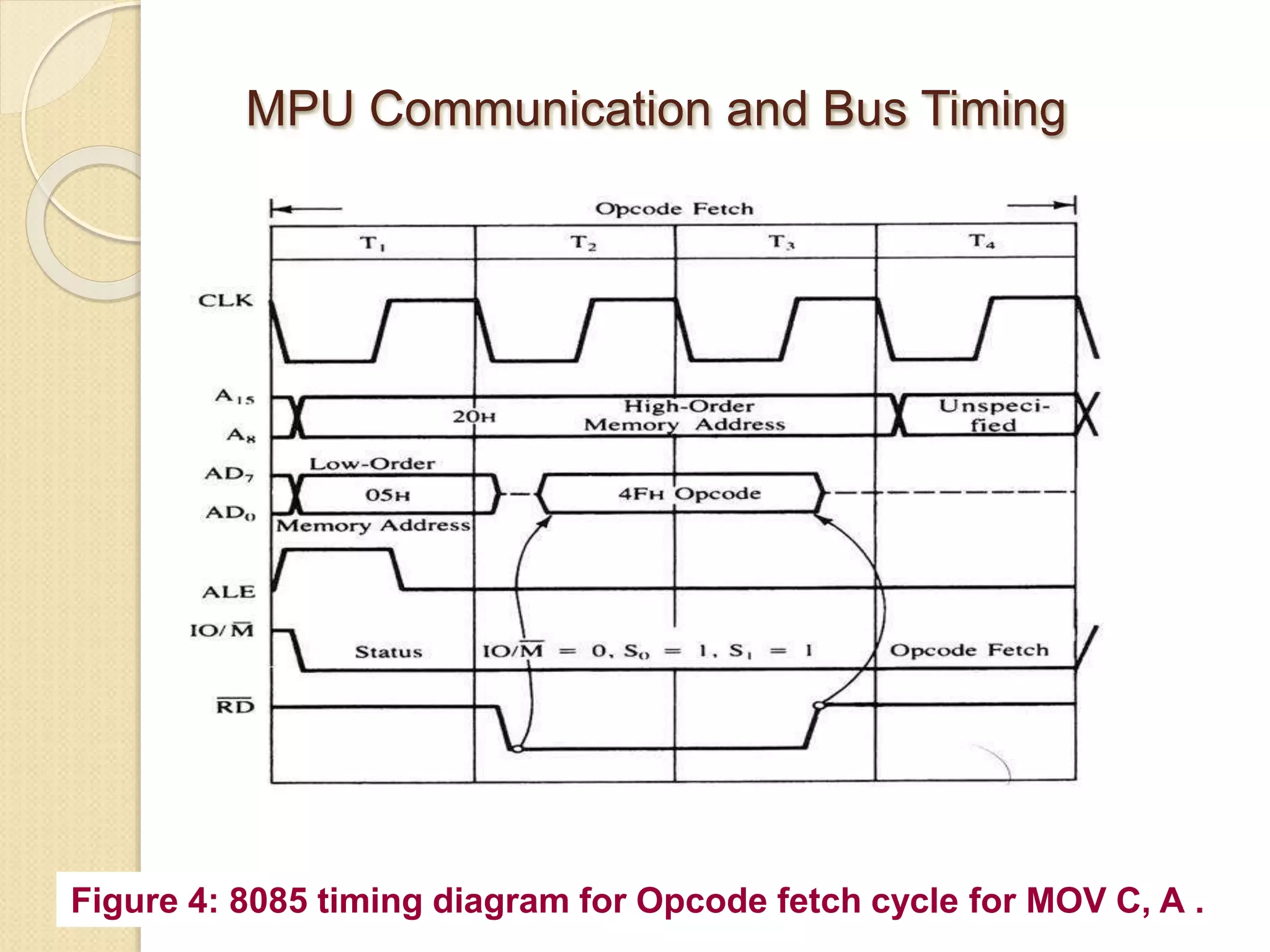
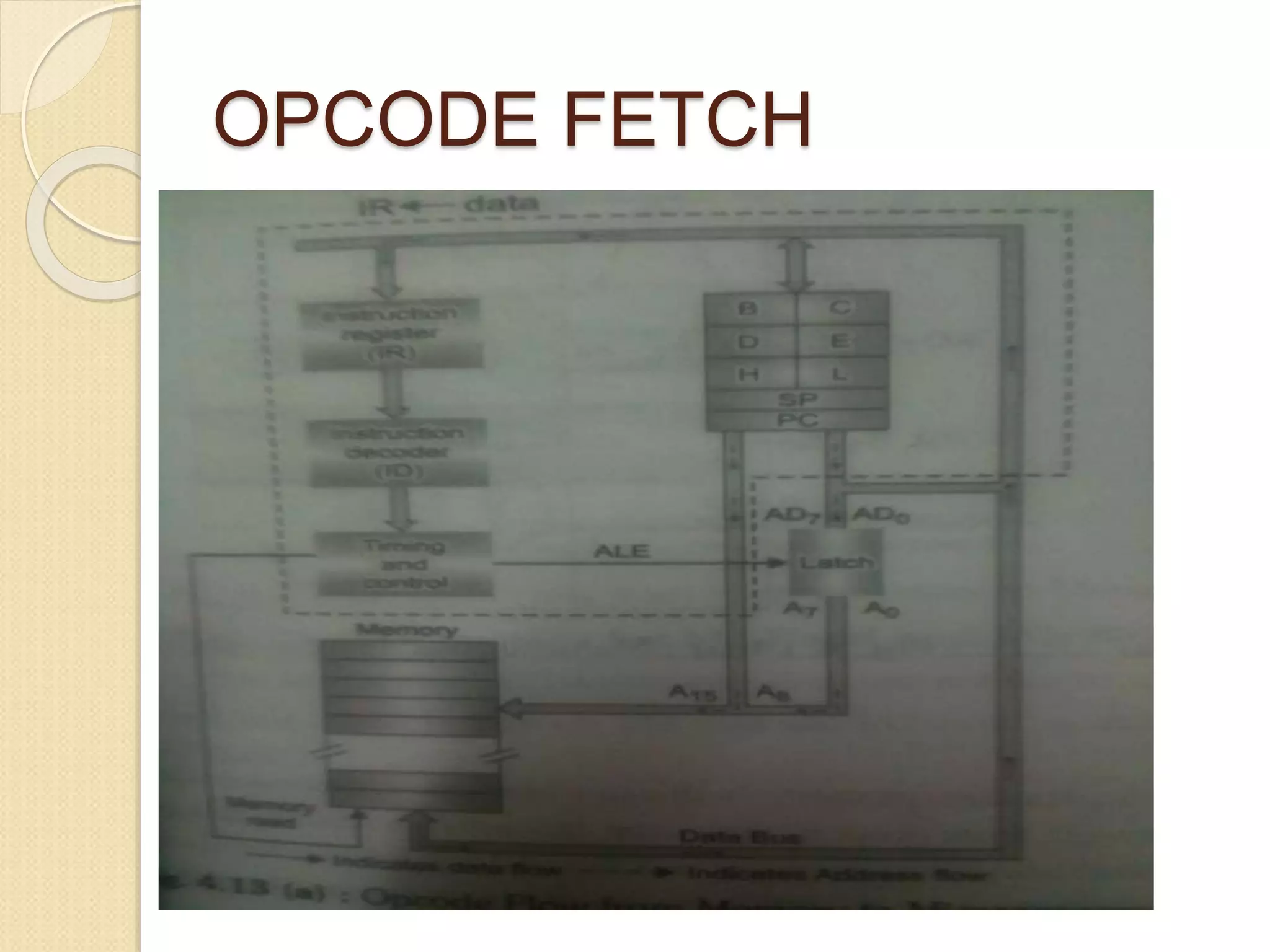
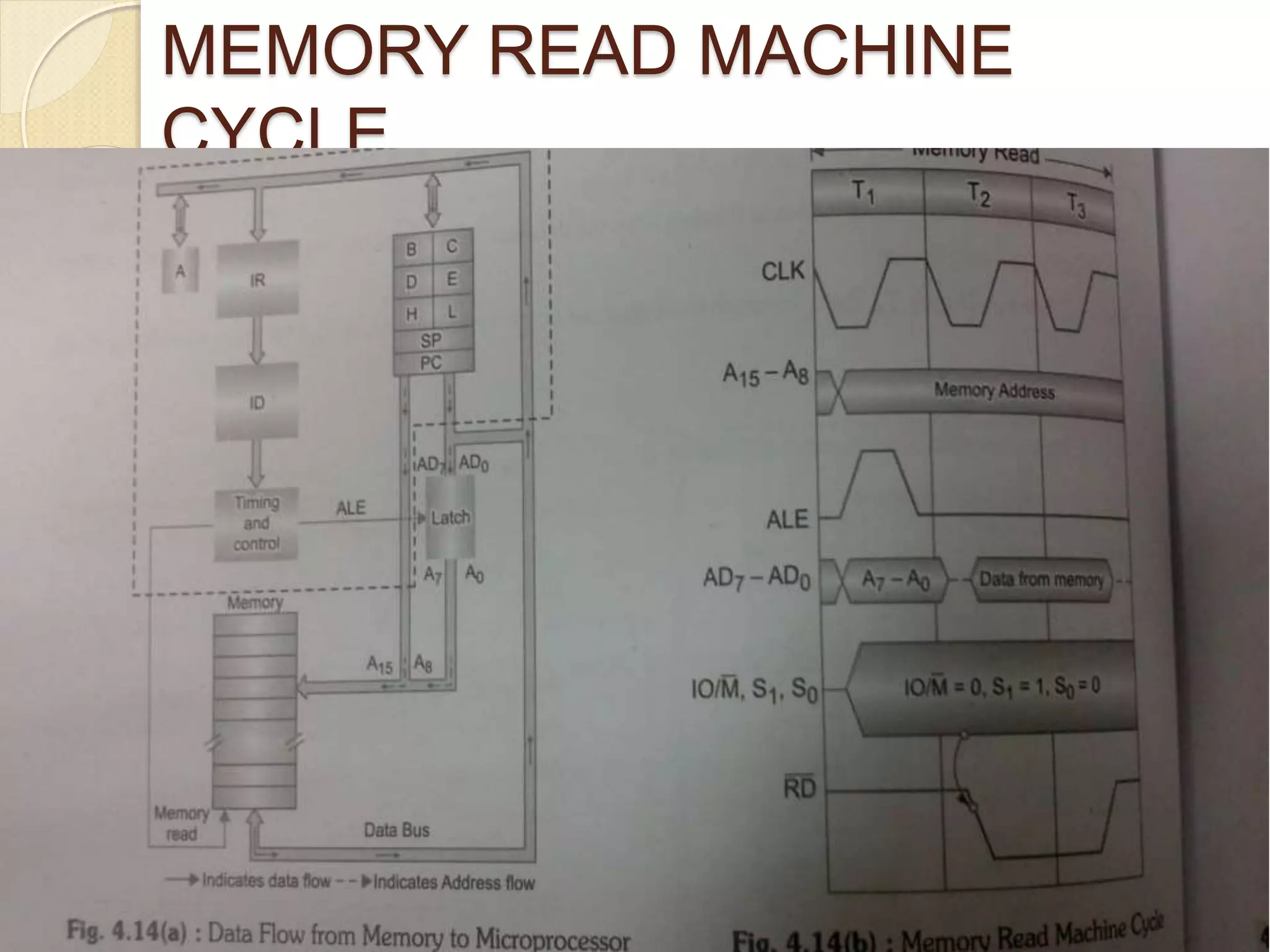
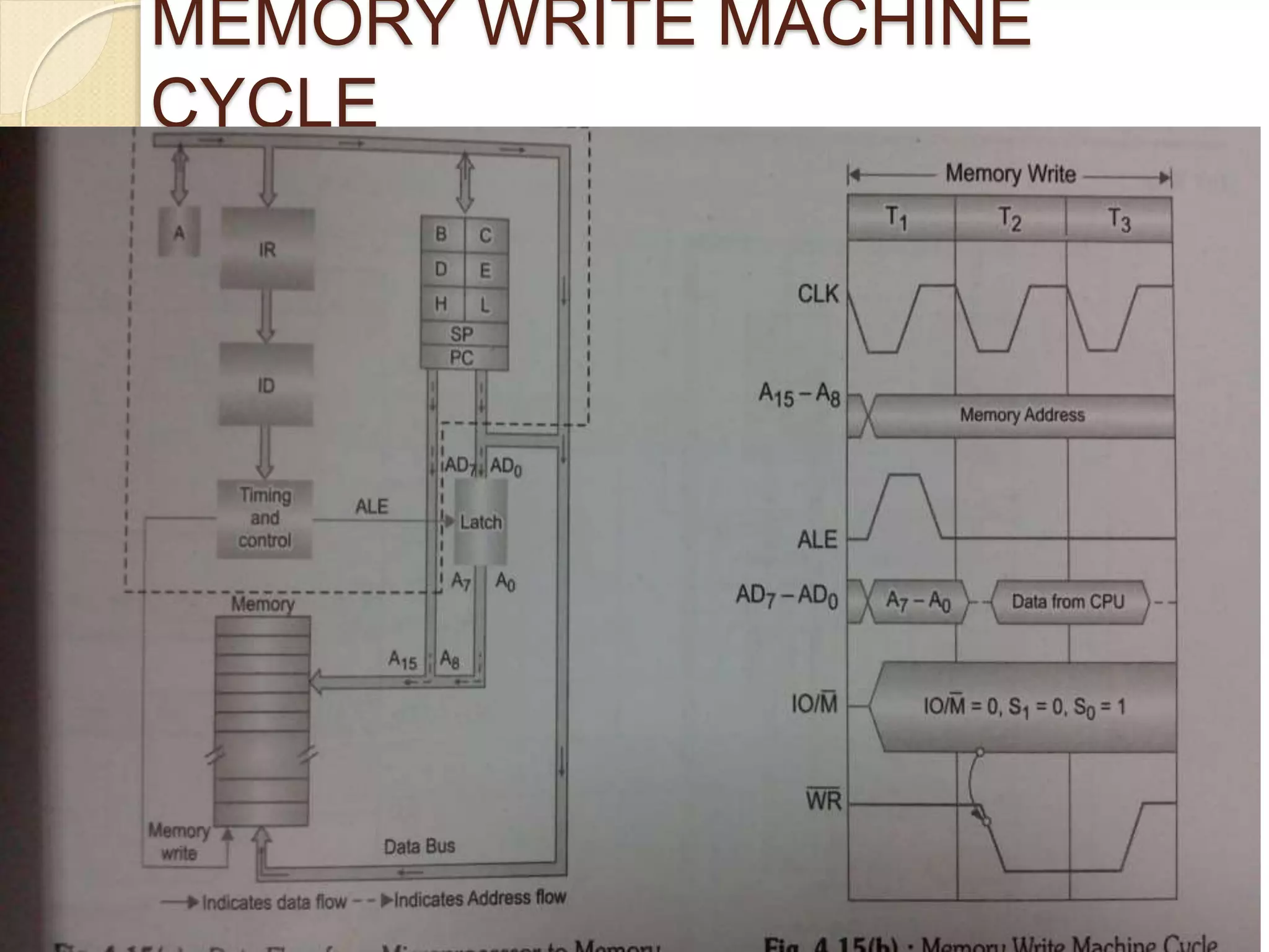
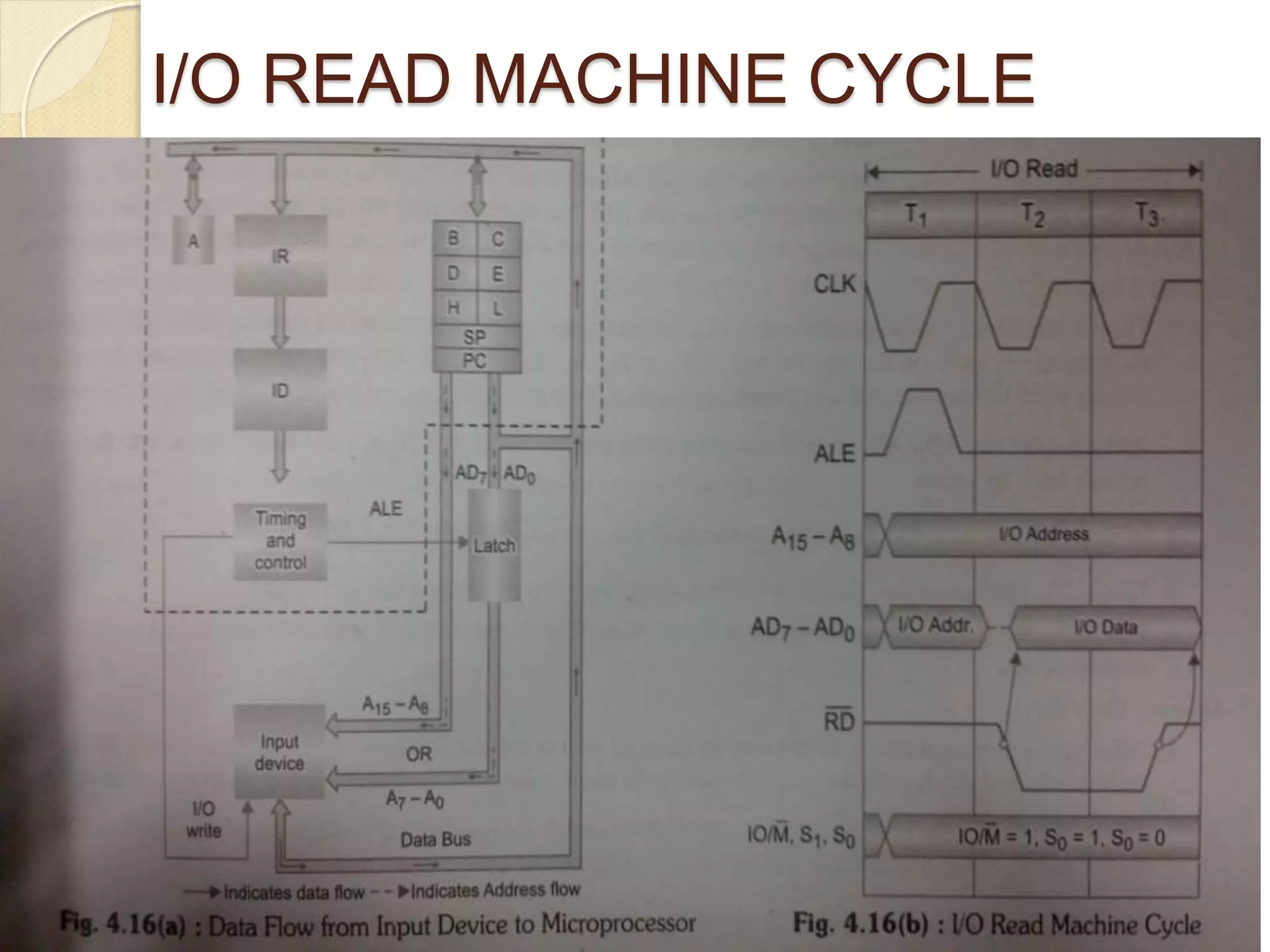
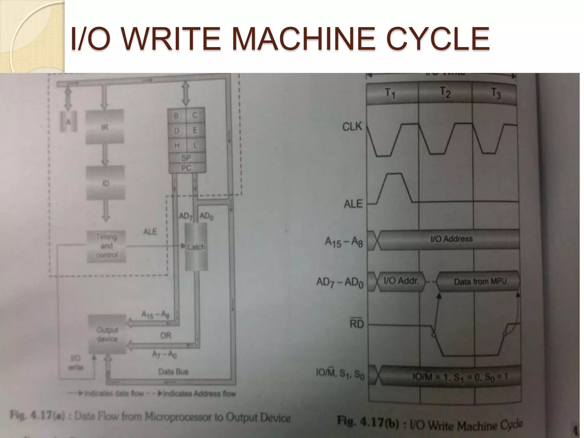
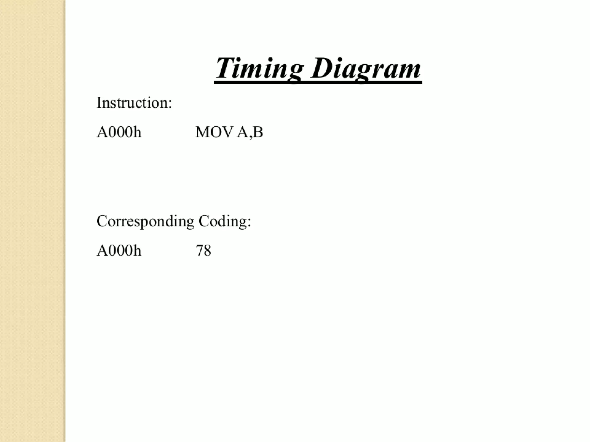
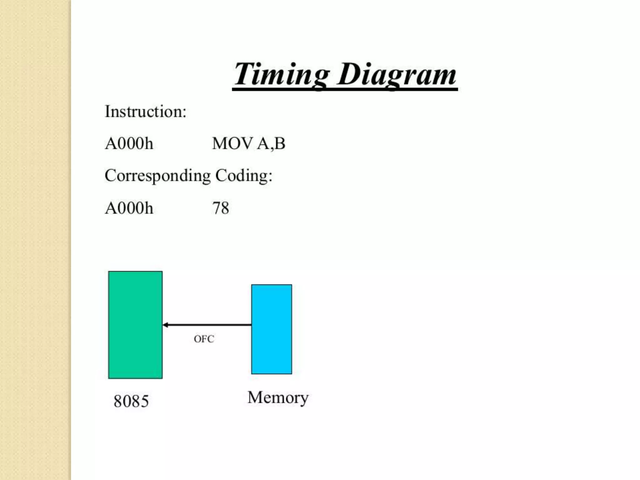
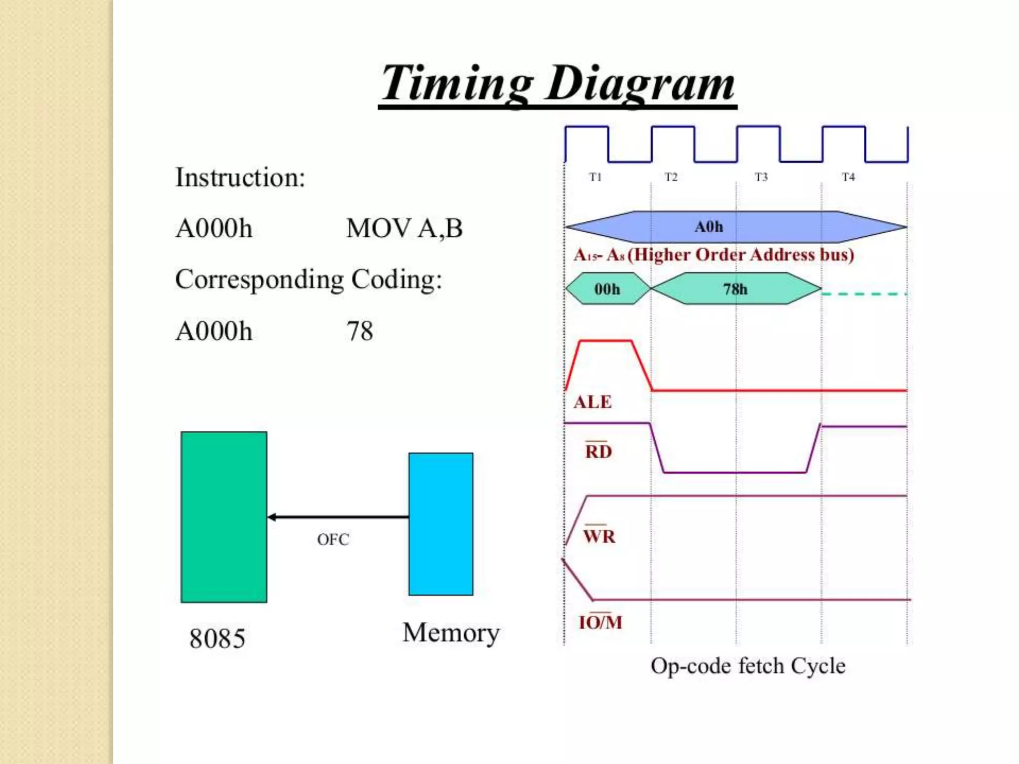
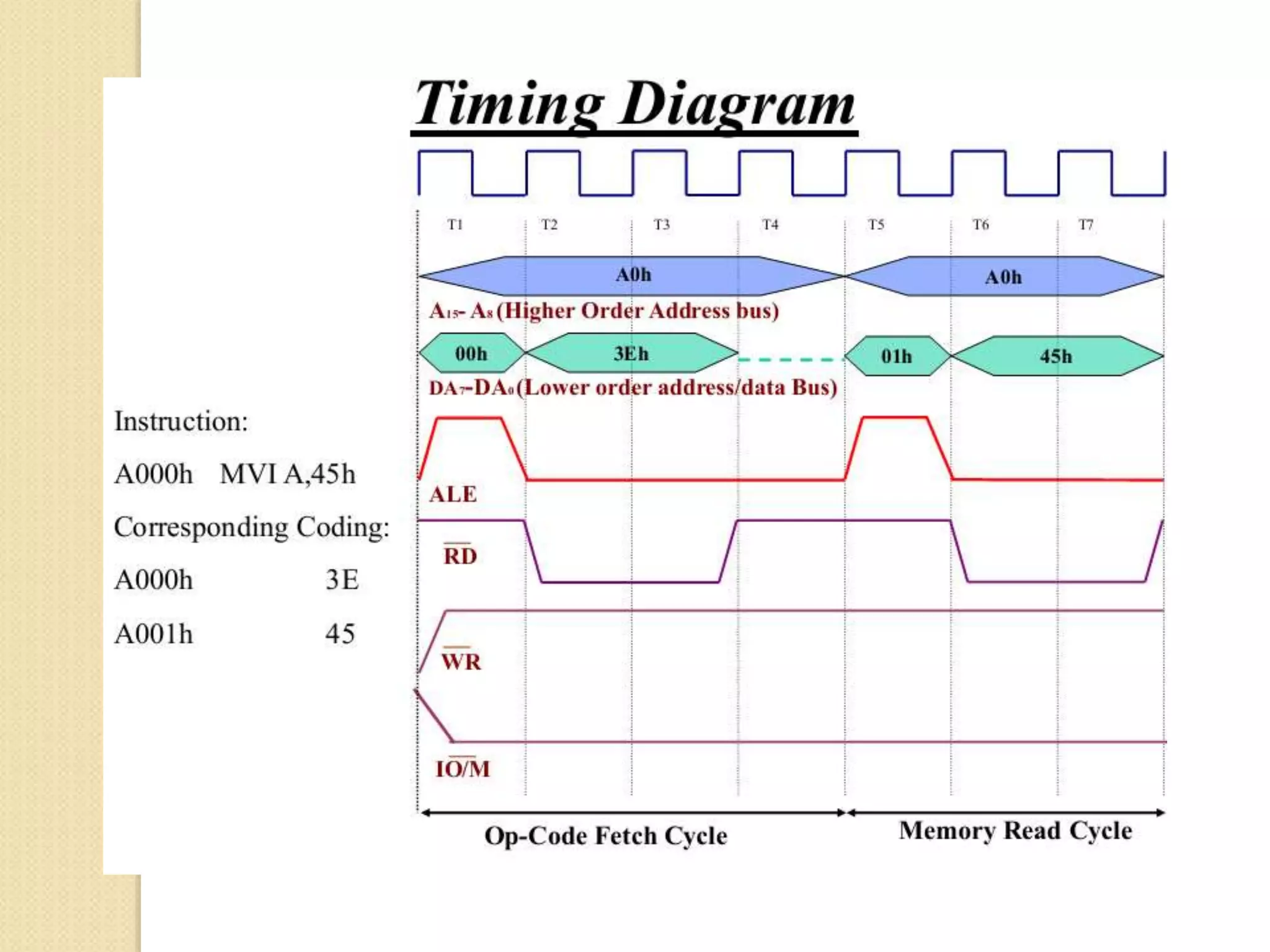
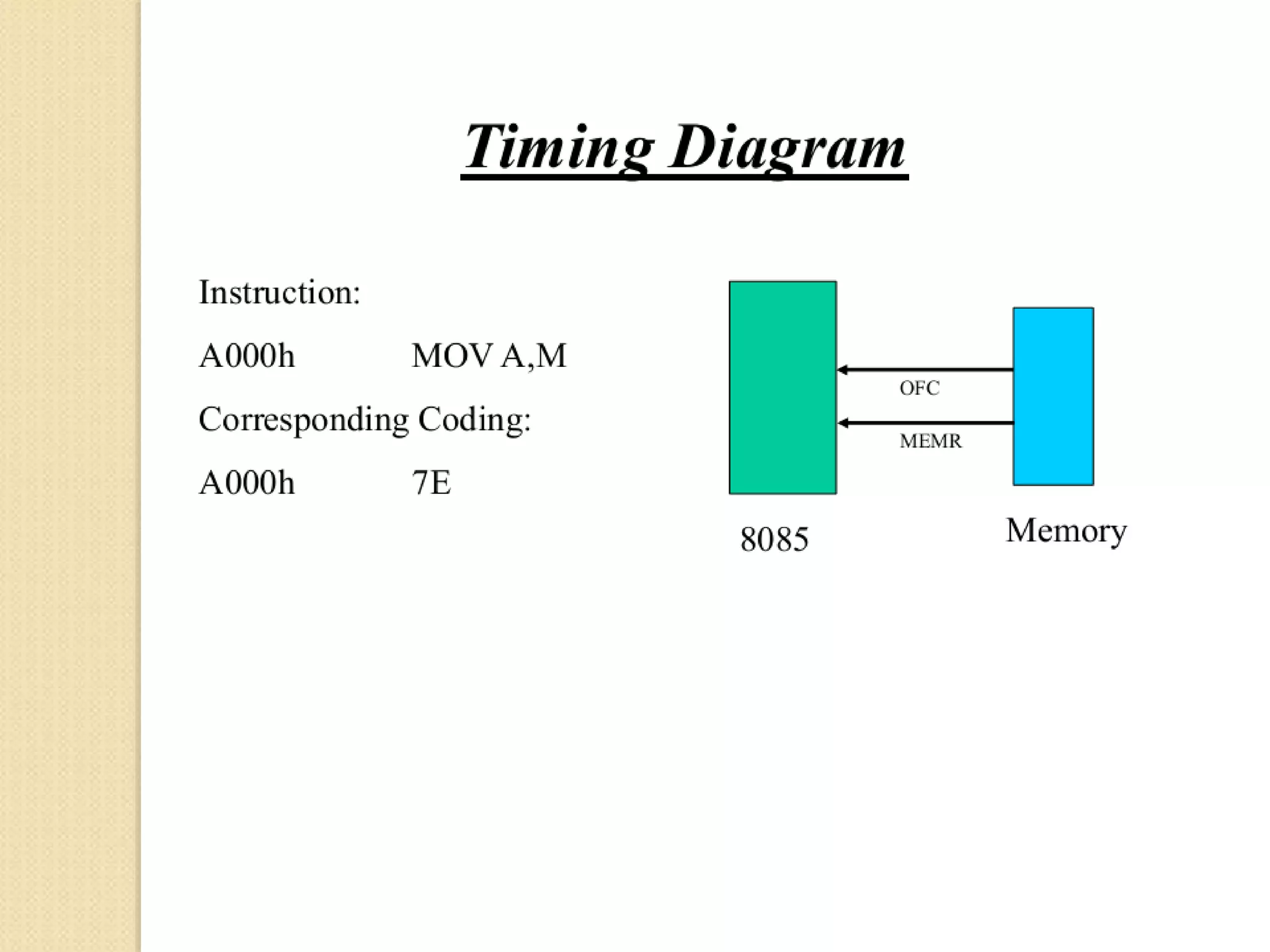
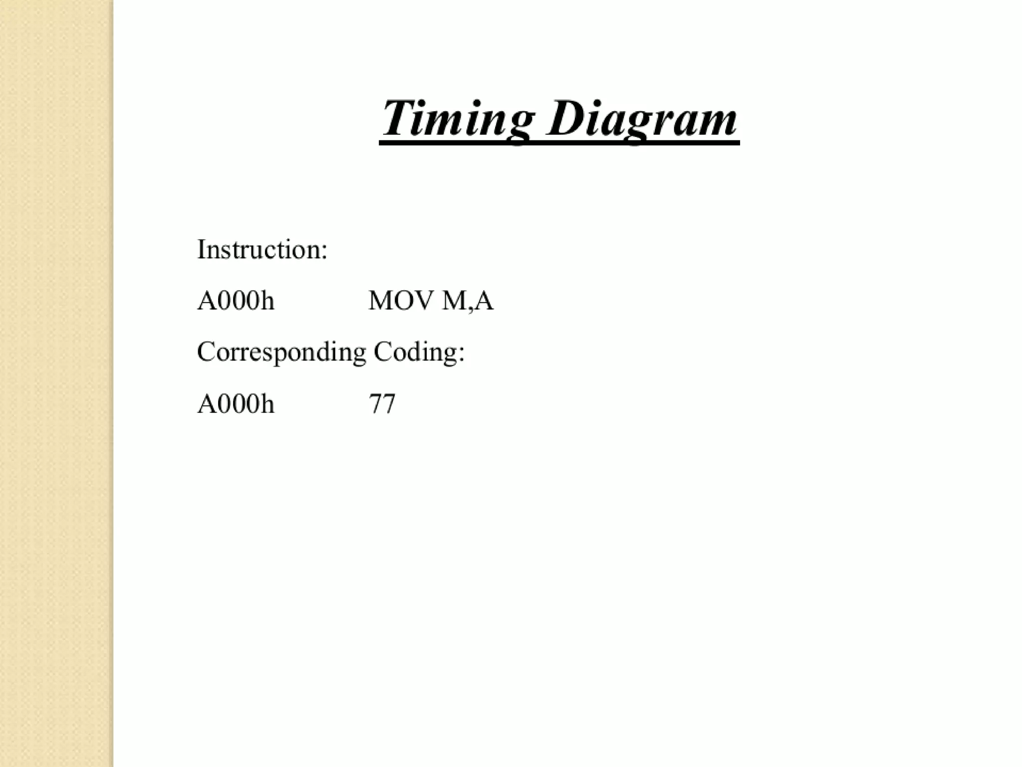
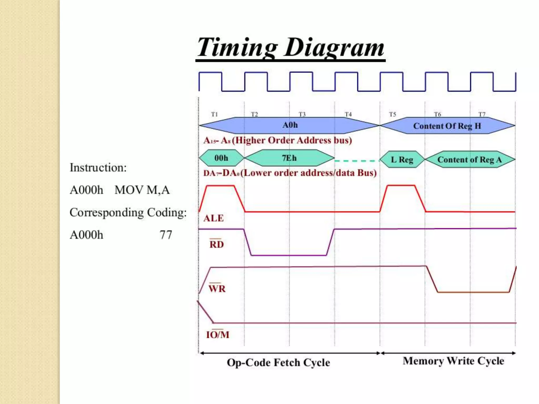
The document describes the fetch-execute cycle of a microprocessor. It has the following key points:
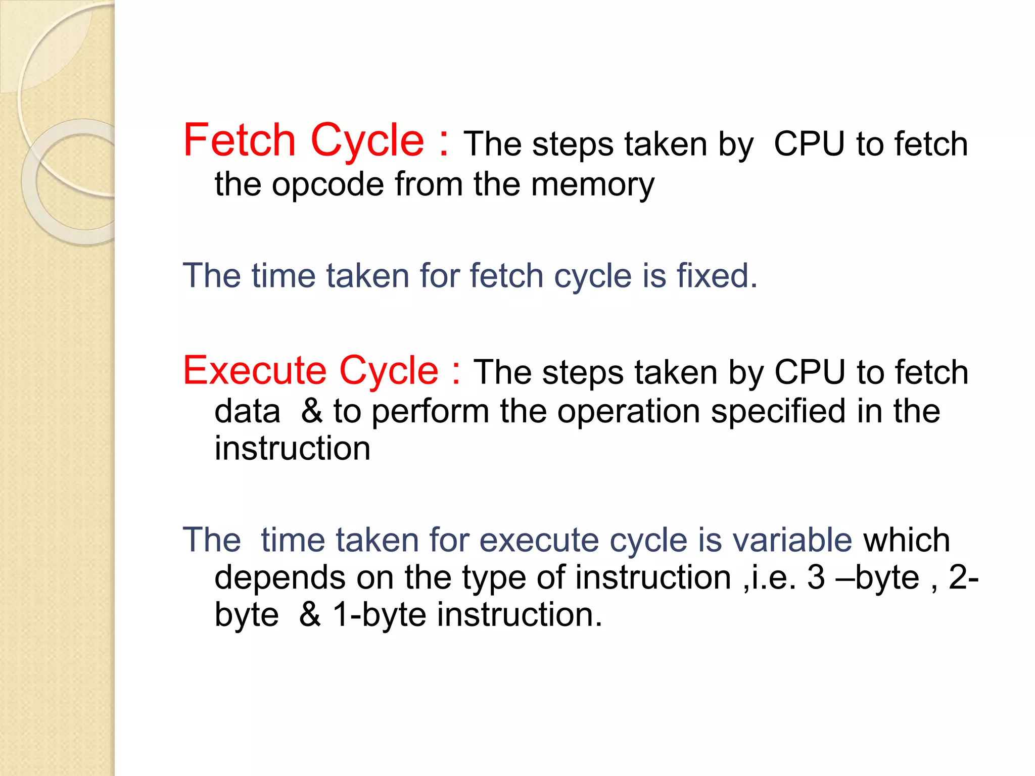
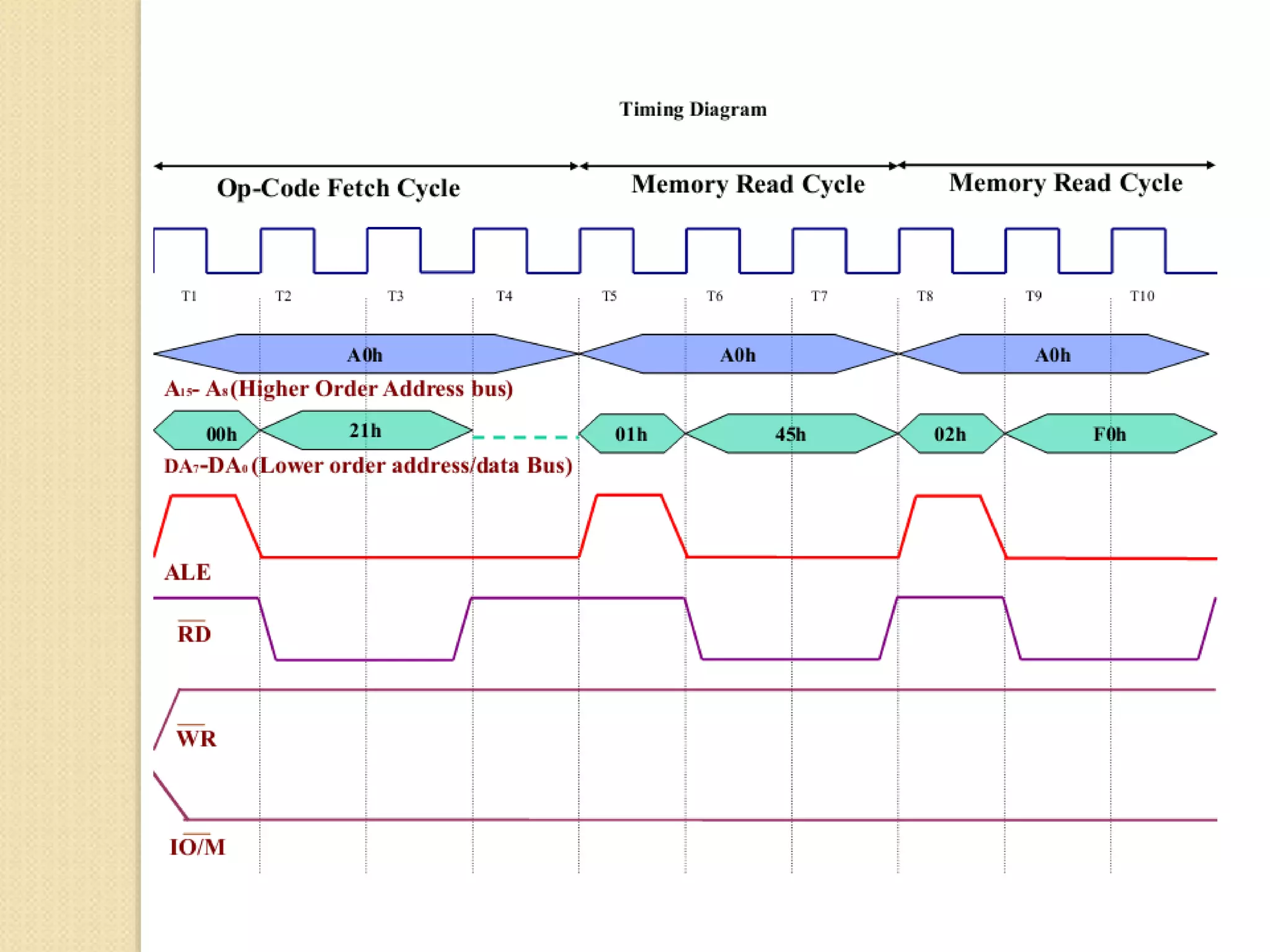
1. The CPU fetches instructions one at a time from memory and executes them. This involves a fetch cycle to retrieve the instruction from memory followed by an execute cycle to perform the operation.
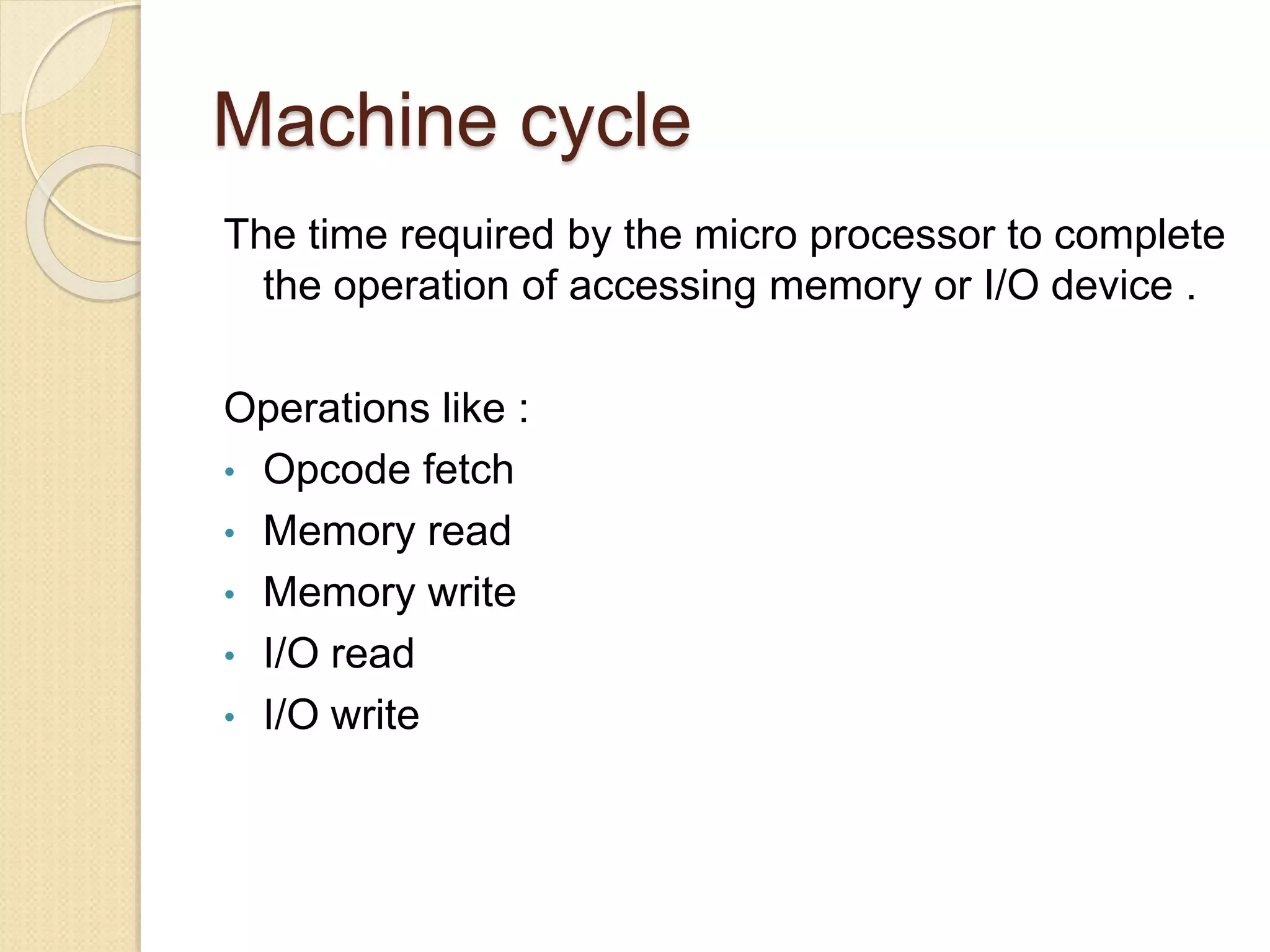
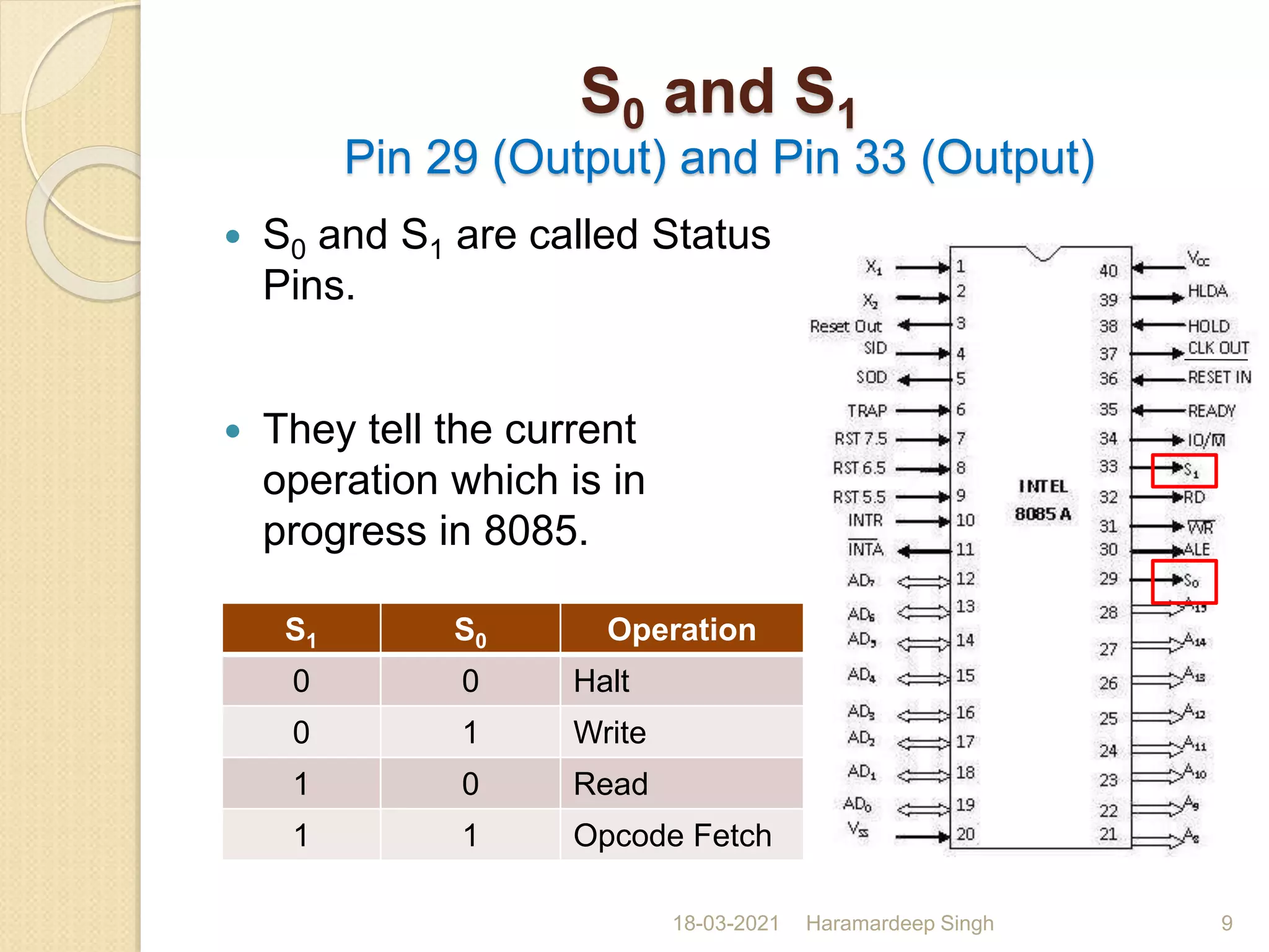
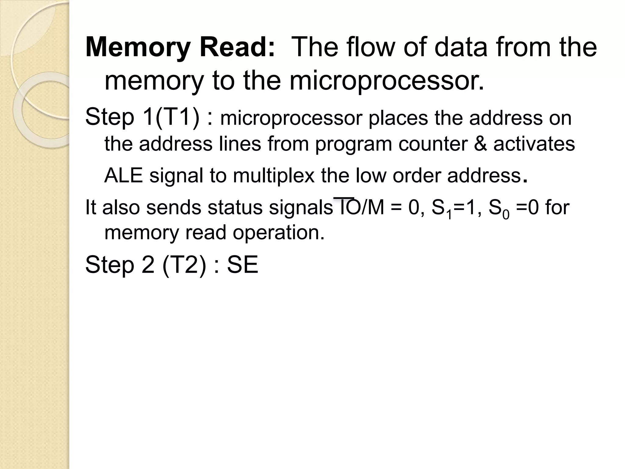
2. During the fetch cycle, the CPU places the memory address on the address bus and activates control signals to retrieve the instruction opcode.
3. The execute cycle involves fetching any required data and performing the operation specified by the instruction, such as moving data between registers or memory. The time taken can vary depending on the instruction type.