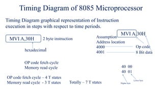
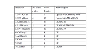
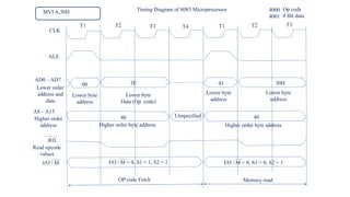
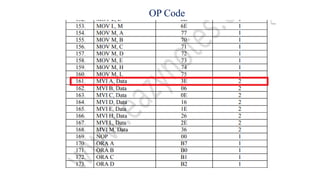
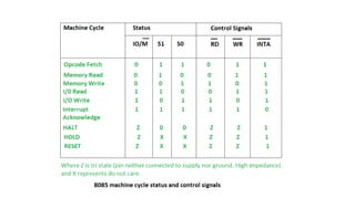
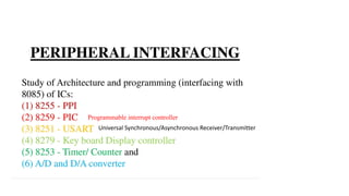
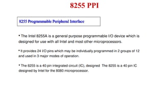
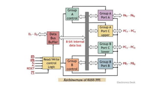
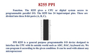
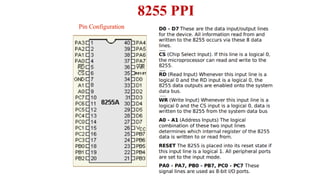
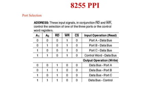
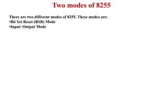
3. Timing Diagram of 8085 Microprocessor
Timing Diagrams of 8085. It is one of the best way to understand to process
of micro-processor/controller. It is the graphical representation of process in
steps with respect to time. The timing diagram represents the clock cycle
and duration, delay, content of address bus and data bus, type of operation
4. Timing Diagram of 8085 Microprocessor
Timing Diagram graphical representation of Instruction
execution in steps with respect to time periods.
MVI A,30H
hexadecimal
2 byte instruction
OP code fetch cycle
Memory read cycle
OP code fetch cycle – 4 T states
Memory read cycle - 3 T states Totally – 7 T states
Assumption
Address location
4000
4001
Op code
MVI A,30H
8 Bit data
40 00
40 01
Lower byte
Higher byte
5.
6. Move a data - Timing Diagram of 8085 Microprocessor
4000
4001
Op code
8 Bit data
7. Timing Diagram of 8085 Microprocessor
T1 T2 T3 T4 T1 T2 T3
CLK
OP code Fetch Memory read
ALE
AD0 – AD7
Lower order
address and
data
Lower byte
address
00 3E
Lower byte
Data (Op code)
MVI A,30H 4000
4001
Op code
8 Bit data
01 30H
A8 – A15
Higher order
address
Lower byte
address
Lower byte
address
Higher order byte address Higher order byte address
40 40Unspecified
RD
Read opcode
values
I/O / M I/O / M = 0, S1 = 1, S2 = 1 I/O / M = 0, S1 = 0, S2 = 1
9. OP Code
In computing, an opcode is the portion of a machine language instruction
that specifies the operation to be performed. Beside the opcode itself, most
instructions also specify the data they will process,
14. Why this PPI?
The 8255 is a general purpose programmable IO device. It is designed to
interface the CPU with some external devices like ADC, DAC, keyboard etc.
We can program the device according to the given condition.
There are three 8-bit bi-directional IO ports. The Port-A, Port-B and Port-C.
These ports are assigned as input or output port.
15.
16.
17. Function. The 8255 gives a CPU or digital system access to
programmable parallel I/O. The 8255 has 24 input/output pins. These are
divided into three 8-bit ports (A, B, C).
8255 PPI
PPI 8255 is a general purpose programmable I/O device designed to
interface the CPU with its outside world such as ADC, DAC, keyboard etc. We
can program it according to the given condition. It can be used with almost any
microprocessor