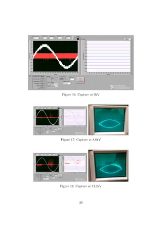
This document describes the making of a partial discharge (PD) data acquisition system based on a National Instruments USB digitizer (NI-5133). The system was developed to measure PDs in insulation systems and present the data graphically using phase resolved analysis. Hardware choices and software development in LabVIEW are discussed. The acquisition system was tested using artificially generated pulses and compared to measurements from a Haefley PD568 system.


![1 Background
Measurement and analysis of partial discharge (PD) is an essential tool for
diagnosis of insulation condition [1]. As the High voltage devices ages, the
insulation tends to become weak which could lead to breakdowns due to
various phenomenon occurring inside the device, raising the risk of insulation
failure, which could be disastrous. Thus it becomes imperative to have a
system that enables analysis of potential insulation problems so that the
devices may be repaired or replaced well in advance.
To analyze the PD’s the magnitude of discharge is measured. Furthermore
the phase position (ϕ) when the discharge takes place during the sinosoidal
voltage period is measured. When the PD magnitude (q) is plotted against
the phase angle the PD pattern is obtained. This pattern is what characterise
a certain type of partial discharge. Traditionally this is done with an analog
PD pattern analyzer but as most modern systems today usually run digitally,
a way to analyze PD patterns digitally is therefore desirable.
2 Aim of the project
The Aim of the project is to develop a portable, digital system for partial
discharge acquisition using an analogue input from hardware such as Haefely
PD568.
1](https://image.slidesharecdn.com/ddf507b9-387c-4e9a-b3a6-8e8cda597dcf-150907103754-lva1-app6891/85/Making-of-a-PD-Data-Acqusition-System-5-320.jpg)
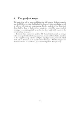
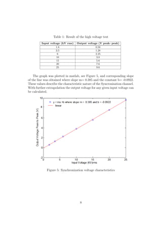
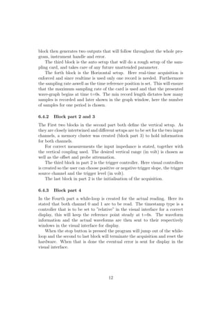
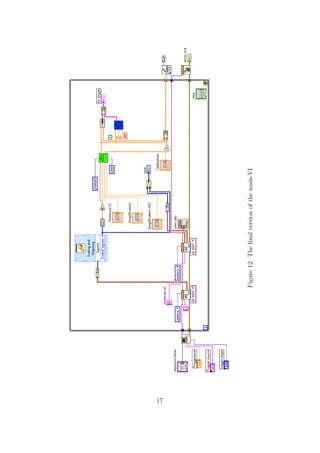
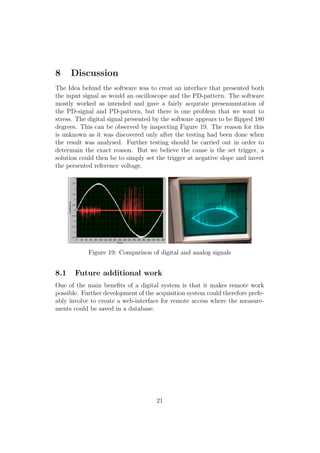
![5.0.1 Phase resolved analysis
Analysis based on phase resolved technique depicts the type of defect and
the level of insulation degradation reached. This is done with the help of
analyzing the discharge occurrence pattern over the power line sinusoidal
wave. This type of distribution is known as the ”fingerprint of a discharge”.
This plays an important role in identifying the kind of defect present in
insulation and the level of deterioration. A typical PD-pattern is presented
in Figure 2.
Figure 2: A typical PD-pattern recieved with the phase resolve method [1]
5](https://image.slidesharecdn.com/ddf507b9-387c-4e9a-b3a6-8e8cda597dcf-150907103754-lva1-app6891/85/Making-of-a-PD-Data-Acqusition-System-9-320.jpg)
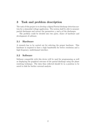
![6 Method
The development was divided into two parts. First proper hardware were to
be chosen. Second the software to run the hardware were to be developed.
6.1 Choice of Hardware
As explained in Section 3, the digital PD-acquisition system needs to have
the capability to sample and store data to characterize PD’s. It should also
be capable of transferring the data obtained to the host PC’s random access
memory to generate (ϕ, q) plots.
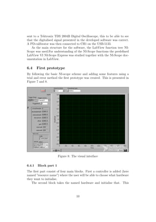
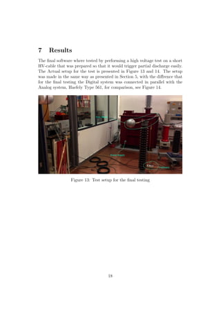
NI USB- 5133 digitizer fulfills all the needs required for this system.
Figure 3: The NI USB-5133 digitizer [2]
The main factors that were considered while selecting digitizer were the
sampling rate, which for the USB-5133 is 100 MS/s. That assures a truthful
reproduction of the analog signal to digital. The bandwidth of 50 MHz and
2 simultaneously sampled channels with 8-bit resolution makes it an ideal
choice. It is having 8 Mb memory equally divided between two channels
CH1 and CH2. The bus powered, plug and play feature of this device makes
it portable and easy to use.
As presented in Figure 1, the USB digitizer would be connected to the the
synchronizing port of the quadripole via channel CH0 or CH1. The digitizer
is having an operating voltage range of 40 Vp−p, i.e. from -20V to +20V. In
6](https://image.slidesharecdn.com/ddf507b9-387c-4e9a-b3a6-8e8cda597dcf-150907103754-lva1-app6891/85/Making-of-a-PD-Data-Acqusition-System-10-320.jpg)
![References
[1] J.A. Ardila-Rey et. al. A Partial Discharges Acquisition and Statistical
Analysis Software. 2012.
[2] url: http://sine.ni.com/nips/cds/view/p/lang/sv/nid/203720.
22](https://image.slidesharecdn.com/ddf507b9-387c-4e9a-b3a6-8e8cda597dcf-150907103754-lva1-app6891/85/Making-of-a-PD-Data-Acqusition-System-26-320.jpg)