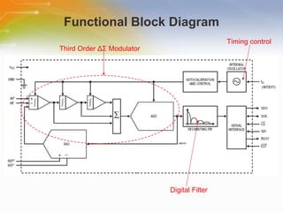
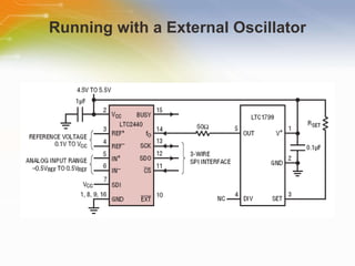
LTC2440 – High Speed Delta Sigma ADC Source: LINEAR TECHNOLOGY
Introduction Purpose This training module introduces the internal architecture of the LTC2440, its basic operation and key features. Outline General introduction & internal functional block diagram Basic operations Key features and design considerations Content 17 pages
General Description Up to 3.5kHz output rate  Selectable speed/resolution  2µV RMS  noise at 880Hz output rate  200nV RMS  noise at 6.9Hz output rate with simultaneous 50/60Hz rejection  0.0005% INL, no missing codes  Autosleep enables 20µA operation at 6.9Hz  < 5µV Offset (4.5V < VCC < 5.5V, –40°C to 85°C)  Differential input and differential reference with GND to VCC common mode range  No Latency, each conversion is accurate even after an input step  Internal oscillator — No external components  In narrow 16-Lead SSOP package
Functional Block Diagram Timing control Third   Order   ΔΣ   Modulator Digital Filter
Serial Interface SCK – synchronize the data transfer Each bit of the conversion result is shifted out on SDO pin on the falling edge of the SCK. SDO – output a serial bit stream  This pin is used as an end of conversion indicator during the conversion and sleep states. CS – enables the SDO digital output and wakes up the ADC The CS signal can be used to trigger a new conversion cycle before the entire serial data transfer has been completed. SDI – select the speed/resolution of the converter BUSY - Conversion in Progress Indicator It is used to monitor the state of conversion, data output and sleep cycle. EXT – Internal/External SCK selection The internal or external SCK mode is selected by tying EXT LOW   for external SCK and HIGH for internal SCK.
SDI Speed/Resolution Programming Logic level speed selection A simple 2-speed control is selectable by either driving SDI HIGH (6.9Hz) or LOW (880Hz). Serial input speed selection SDI may also be programmed by a serial input data stream under control of SCK during the data output cycle
Converter Operation Cycle Its operation is made up of three states Conversion Low power sleep state Data output
Timing Modes External Serial Clock, Single Cycle Conversion It uses an external serial clock to shift out the conversion result. CS signal is to monitor and control the state of the conversion cycle. External Serial Clock, 2-Wire I/O The conversion result is shifted out of the device by an externally generated serial clock (SCK) signal. Internal Serial Clock, Single Cycle Operation It uses an internal serial clock to shift out the conversion result. CS signal to monitor and control the state of the conversion cycle. Internal Serial Clock, Continuous Conversion The conversion result is shifted out of the device by an internally generated serial clock (SCK) signal.
Output Data Format Bit 31: End of conversion indicator Bit 30: Dummy bit and always LOW Bit 29: Conversion result sign indicator Bit 28: the most significant bit of the result Bit 28 to 5: 24-bit conversion result Bit 4 to 0: sub LSBs below the 24-bit level Underrange or Overrange indication
Reduced Power Operation The user may reduce the DC power dissipation by extending the duration of the low power sleep state extending the duration of  the conversion cycle
Normal Mode Rejection and Antialiasing An on chip digital low pass filter offers excellent rejection up to the internal modulator sampling rate. At multiples of the internal modulator sample rate, unwanted input perturbations are folded back to DC with little attenuation (aliasing).  Normal Mode Rejection (Internal Oscillator) Normal Mode Rejection (External Oscillator @ 90kHz)
Measuring Low Level Signals without a PGA Eliminating the PGA (and tare adjust) requires a converter with  Exceptional offset High linearity Full-scale accuracy Low drift Low noise The number of counts produced  over the full output range typically determines performance. Speed vs. RMS Noise
Direct Connection to Low Impedance Sources Long connection to low impedance sources Short connection to low impedance sources Figure 1 Figure 2
Buffering the LTC2440 A general procedure for evaluating the suitability of an amplifier for use as a buffer with the LTC2440 is suggested Perform a thorough error and noise analysis on the amplifier and gain setting components to verify that the amplifier will perform as intended. Measure the large signal response of the overall circuit. Verify that the slew rate is adequate for the fastest expected input signal. Measure noise performance of the complete circuit. Verify that the noise is as expected, taking into account the bandwidth of the LTC2440 inputs for the OSR being used.
Running with a External Oscillator
Summary The LTC2440 offers accuracy, stability, and ease of use. It combines a programmable OSR digital filter with a high speed analog modulator in order to achieve high speed and accuracy.  The LTC2440’s wide range of user programmable speed and resolution combinations makes it fit in a wide variety of applications.  High Speed Multiplexing  Weight Scales  Auto Ranging 6-Digit DVMs  Direct Temperature Measurement  High Speed Data Acquisition
Additional Resource For ordering the LTC2440 ADC, please click the part list or Call our sales hotline For additional inquires contact our technical service hotline For more product information go to http://www.linear.com/pc/productDetail.jsp?navId=H0,C1,C1155,C1001,C1152,P1771 Newark Farnell

LTC2440 - High Speed Delta Sigma ADC

  • 1.
    LTC2440 – HighSpeed Delta Sigma ADC Source: LINEAR TECHNOLOGY
  • 2.
    Introduction Purpose Thistraining module introduces the internal architecture of the LTC2440, its basic operation and key features. Outline General introduction & internal functional block diagram Basic operations Key features and design considerations Content 17 pages
  • 3.
    General Description Upto 3.5kHz output rate Selectable speed/resolution 2µV RMS noise at 880Hz output rate 200nV RMS noise at 6.9Hz output rate with simultaneous 50/60Hz rejection 0.0005% INL, no missing codes Autosleep enables 20µA operation at 6.9Hz < 5µV Offset (4.5V < VCC < 5.5V, –40°C to 85°C) Differential input and differential reference with GND to VCC common mode range No Latency, each conversion is accurate even after an input step Internal oscillator — No external components In narrow 16-Lead SSOP package
  • 4.
    Functional Block DiagramTiming control Third Order ΔΣ Modulator Digital Filter
  • 5.
    Serial Interface SCK– synchronize the data transfer Each bit of the conversion result is shifted out on SDO pin on the falling edge of the SCK. SDO – output a serial bit stream This pin is used as an end of conversion indicator during the conversion and sleep states. CS – enables the SDO digital output and wakes up the ADC The CS signal can be used to trigger a new conversion cycle before the entire serial data transfer has been completed. SDI – select the speed/resolution of the converter BUSY - Conversion in Progress Indicator It is used to monitor the state of conversion, data output and sleep cycle. EXT – Internal/External SCK selection The internal or external SCK mode is selected by tying EXT LOW for external SCK and HIGH for internal SCK.
  • 6.
    SDI Speed/Resolution ProgrammingLogic level speed selection A simple 2-speed control is selectable by either driving SDI HIGH (6.9Hz) or LOW (880Hz). Serial input speed selection SDI may also be programmed by a serial input data stream under control of SCK during the data output cycle
  • 7.
    Converter Operation CycleIts operation is made up of three states Conversion Low power sleep state Data output
  • 8.
    Timing Modes ExternalSerial Clock, Single Cycle Conversion It uses an external serial clock to shift out the conversion result. CS signal is to monitor and control the state of the conversion cycle. External Serial Clock, 2-Wire I/O The conversion result is shifted out of the device by an externally generated serial clock (SCK) signal. Internal Serial Clock, Single Cycle Operation It uses an internal serial clock to shift out the conversion result. CS signal to monitor and control the state of the conversion cycle. Internal Serial Clock, Continuous Conversion The conversion result is shifted out of the device by an internally generated serial clock (SCK) signal.
  • 9.
    Output Data FormatBit 31: End of conversion indicator Bit 30: Dummy bit and always LOW Bit 29: Conversion result sign indicator Bit 28: the most significant bit of the result Bit 28 to 5: 24-bit conversion result Bit 4 to 0: sub LSBs below the 24-bit level Underrange or Overrange indication
  • 10.
    Reduced Power OperationThe user may reduce the DC power dissipation by extending the duration of the low power sleep state extending the duration of the conversion cycle
  • 11.
    Normal Mode Rejectionand Antialiasing An on chip digital low pass filter offers excellent rejection up to the internal modulator sampling rate. At multiples of the internal modulator sample rate, unwanted input perturbations are folded back to DC with little attenuation (aliasing). Normal Mode Rejection (Internal Oscillator) Normal Mode Rejection (External Oscillator @ 90kHz)
  • 12.
    Measuring Low LevelSignals without a PGA Eliminating the PGA (and tare adjust) requires a converter with Exceptional offset High linearity Full-scale accuracy Low drift Low noise The number of counts produced over the full output range typically determines performance. Speed vs. RMS Noise
  • 13.
    Direct Connection toLow Impedance Sources Long connection to low impedance sources Short connection to low impedance sources Figure 1 Figure 2
  • 14.
    Buffering the LTC2440A general procedure for evaluating the suitability of an amplifier for use as a buffer with the LTC2440 is suggested Perform a thorough error and noise analysis on the amplifier and gain setting components to verify that the amplifier will perform as intended. Measure the large signal response of the overall circuit. Verify that the slew rate is adequate for the fastest expected input signal. Measure noise performance of the complete circuit. Verify that the noise is as expected, taking into account the bandwidth of the LTC2440 inputs for the OSR being used.
  • 15.
    Running with aExternal Oscillator
  • 16.
    Summary The LTC2440offers accuracy, stability, and ease of use. It combines a programmable OSR digital filter with a high speed analog modulator in order to achieve high speed and accuracy. The LTC2440’s wide range of user programmable speed and resolution combinations makes it fit in a wide variety of applications. High Speed Multiplexing Weight Scales Auto Ranging 6-Digit DVMs Direct Temperature Measurement High Speed Data Acquisition
  • 17.
    Additional Resource Forordering the LTC2440 ADC, please click the part list or Call our sales hotline For additional inquires contact our technical service hotline For more product information go to http://www.linear.com/pc/productDetail.jsp?navId=H0,C1,C1155,C1001,C1152,P1771 Newark Farnell

Editor's Notes

  • #3 Welcome to the training module on Linear Technology LTC2440 – High Speed Delta Sigma ADC. This training module introduces the internal architecture of the LTC2440, its basic operation and key features.
  • #4 The LTC2440 is a high speed 24-bit No Latency Delta Sigma ADC with 5ppm INL and 5µV offset. It uses proprietary Delta Sigma architecture enabling variable speed and resolution with no latency. Ten speed/resolution combinations (6.9Hz/ 200nVRMS to 3.5kHz/25µVRMS) are programmed through a simple serial interface. Alternatively, by tying a single pin HIGH or LOW, a fast (880Hz/2µVRMS) or ultralow noise (6.9Hz, 200nVRMS, 50/60Hz rejection) speed/resolution combination can be easily selected. The accuracy (offset, full-scale, linearity, drift) and power dissipation are independent of the speed selected. Since there is no latency, a speed/resolution change may be made between conversions with no degradation in performance. Following each conversion cycle, the LTC2440 automatically enters a low power sleep state. Power dissipation may be reduced by increasing the duration of this sleep state. The LTC2440 communicates through a flexible 3-wire or 4-wire digital interface.
  • #5 The LTC2440 is a high speed, delta-sigma analog-to-digital converter with an easy to use 4-wire serial interface. The 4-wire interface consists of serial data input (SDI), serial data output (SDO), serial clock (SCK) and chip select (CS). The interface, timing, operation cycle and data out format is compatible with the LTC2410. SDI pin is used to select the speed / resolution of the converter. During the data output period, the SDO pin is used as serial data output. During the Conversion and Sleep periods, this pin is used as the conversion status output. The voltage on the differential analog pins can have any value between GND-0.3V and VCC+0.3V. Within these limits the converter bipolar input range (V IN = IN+ – IN–) extends from –0.5x(VREF) to 0.5x(VREF). Outside this input range the converter produces unique over-range and under-range output codes. The LTC2440 can accept a differential reference voltage from 0.1V to V CC . The LTC2440 performs offset and full-scale calibrations every conversion cycle. The advantage of continuous calibration is extreme stability of offset and full-scale readings with respect to time, supply voltage change and temperature drift.
  • #6 The LTC2440 transmits the conversion results and receives the start of conversion command through a synchronous 2-wire, 3-wire or 4-wire interface. During the conversion and sleep states, this interface can be used to assess the converter status and during the data output state it is used to read the conversion result and program the speed/resolution.
  • #7 The serial data input (SDI, Pin 7) is used to select the speed/resolution of the LTC2440. A simple 2-speed control is selectable by either driving SDI HIGH or LOW. If SDI is grounded the device outputs data at 880Hz with 21 bits effective resolution. By tying SDI HIGH, the converter enters the ultralow noise mode (200nVRMS) with simultaneous 50/60Hz rejection at 6.9Hz output rate. SDI may also be programmed by a serial input data stream under control of SCK during the data output cycle. One of ten speed/resolution ranges from 6.9Hz/200nVRMS to 3.5kHz/21μVRMS may be selected as shown on the table. The conversion following a new selection is valid and performed at the newly selected speed/resolution.
  • #8 Initially, the LTC2440 performs a conversion. Once the conversion is complete, the device enters the sleep state. While in this sleep state, power consumption is reduced below 10μA. The part remains in the sleep state as long as CS is HIGH. The conversion result is held indefinitely in a static shift register while the converter is in the sleep state. Once CS is pulled LOW, the device begins outputting the conversion result. There is no latency in the conversion result. The data output corresponds to the conversion just performed. This result is shifted out on the serial data out pin (SDO) under the control of the serial clock (SCK). Data is updated on the falling edge of SCK allowing the user to reliably latch data on the rising edge of SCK. The data output state is finished once 32-bits are read out of the ADC or when CS is brought HIGH. The device automatically initiates a new conversion and the cycle repeats.
  • #9 The LTC2440’s 2-wire, 3-wire or 4-wire interface is SPI and MICROWIRE compatible. This interface offers several flexible modes of operation. These include internal/external serial clock, 2-wire or 3-wire I/O, single cycle conversion and auto-start.
  • #10 The LTC2440 serial output data stream is 32-bits long. The first 3-bits represent status information indicating the sign and conversion state. The next 24-bits are the conversion result, MSB first. The remaining 5-bits are sub LSBs beyond the 24-bit level that may be included in averaging or discarded without loss of resolution. In the case of ultrahigh resolution modes, more than 24 effective bits of performance are possible. Under these conditions, sub LSBs are included in the conversion result and represent useful information beyond the 24-bit level. The third and fourth bit together are also used to indicate an under-range condition or an over-range condition.
  • #11 During the conversion cycle, the LTC2440 draws 8mA supply current independent of the programmed speed. Once the conversion cycle is completed, the device automatically enters a low power sleep state drawing 8μA. The device remains in this state as long as CS is HIGH and data is not shifted out. By adjusting the duration of the sleep state (hold CS HIGH longer) and the duration of the conversion cycle (programming OSR) the DC power dissipation can be reduced.
  • #12 One of the advantages delta-sigma ADCs offer over conventional ADCs is on-chip digital filtering. Combined with a large oversampling ratio, the LTC2440 significantly simplifies antialiasing filter requirements. The LTC2440’s speed/resolution is determined by the over sample ratio (OSR) of the on-chip digital filter. The OSR ranges from 64 for 3.5kHz output rate to 32,768 for 6.9Hz output rate. The value of OSR and the sample rate f S determine the filter characteristics of the device. Since the OSR is typically large (≥64), the digital filter offers excellent rejection of input noise sources and simple antialiasing requirements.
  • #13 Programmable gain amplifiers (PGAs) are commonly used in systems where a small input signal (RTD, thermocouple, strain gauge) needs to be applied to a wide input range analog-to-digital converter. The convention is to amplify the sensor output voltage range so that it matches the ADC input range. However, the system performance is dominated by the noise performance of the PGA as well as its offset, full-scale, and linearity performance. PGAs degrade the system performance by introducing added error sources drift, cost and complexity. Eliminating the PGA requires a converter with exceptional offset, linearity, full-scale accuracy, drift, and noise performance. The converter requires enough resolution over its full input range to maintain high resolution within a significantly reduced portion of its input span. This allows system designers to directly interface sensors to the ADC while using a small portion of the overall converter input range. The exceptional noise performance of the LTC2440 allows the user to make one conversion with 500,000 counts and no DC errors for any ±50mV range.
  • #14 If the ADC can be located physically close to the sensor, it can be directly connected to sensors or other sources with impedances up to 350Ω with no other components required as shown in Figure 1. If longer lead lengths are unavoidable, adding an input capacitor close to the ADC input pins will average the charging pulses and prevent reflections or ringing as shown in Figure 2.
  • #15 Many applications will require buffering, particularly where high impedance sources are involved or where the device being measured is located some distance from the LTC2440. the figure shows a network suitable for coupling the inputs of a LTC2440 to a LTC2051 chopper-stabilized op amp. The 3μV offset and low noise of the LTC2051 make it a good choice for buffering the LTC2440. The LTC2051 is configured to be able to drive the 1μF capacitors at the inputs of the LTC2440. The 1μF capacitors should be located close to the ADC input pins. Here lists 3 items for selecting a suitable amplifier as a buffer.
  • #16 Running with an external oscillator of 100kHz and the highest resolution (OSR = 32,768), the RMS noise of the LTC2440 is 200nV over a full ±2.5V input range. Six decades of current, in either direction, can be measured accurately through a 1Ω resistor independent of low frequency system noise. The flexible common mode input range enables the LTC2440 to digitize these signals near V DD . The LTC1799 is a precision oscillator which frequency is programmed by a single external resistor.
  • #17 The LTC2440 offers accuracy, stability, and ease of use that are common to the LTC2400 product family. It combines a programmable OSR digital filter with a high speed analog modulator in order to achieve high speed and accuracy independent of output rate. The LTC2440’s wide range of user programmable speed and resolution combinations makes it flexible enough to fit in a wide variety of applications.
  • #18 Thank you for taking the time to view this presentation on “ LTC2440 – High Speed Delta Sigma ADC” . If you would like to learn more or go on to purchase some of these devices, you may either click on the part list link, or simply call our sales hotline. For more technical information you may either visit the Linear Technology site – link shown – or if you would prefer to speak to someone live, please call our hotline number, or even use our ‘live chat’ online facility.