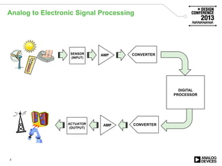
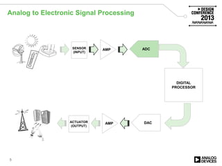
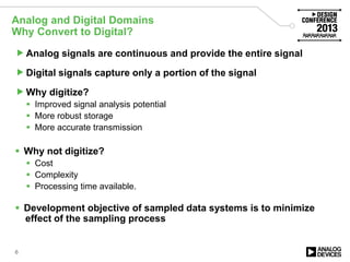
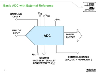
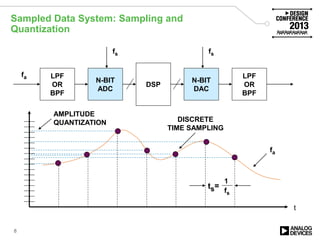
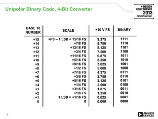
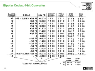
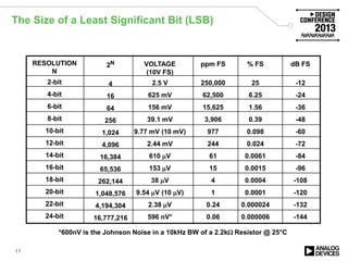
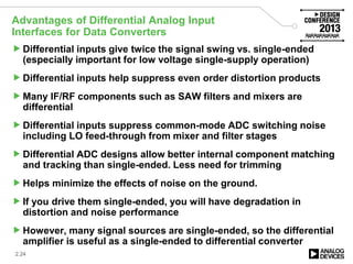
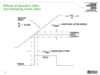
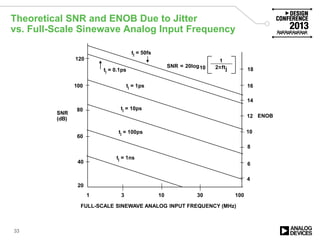
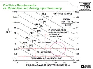
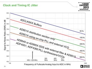
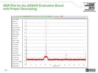
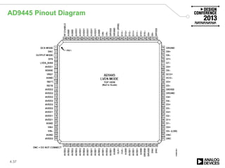
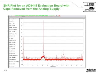
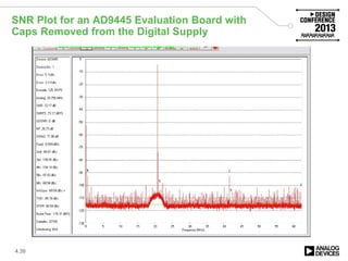
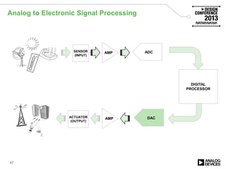
Data Converters for Solving Hard
Problems
Advanced Techniques of Higher Performance Signal Processing
Presenter: Hank Zumbahlen
Legal Disclaimer
 Notice of proprietary information, Disclaimers and Exclusions Of Warranties
The ADI Presentation is the property of ADI. All copyright, trademark, and other intellectual property and
proprietary rights in the ADI Presentation and in the software, text, graphics, design elements, audio and all other
materials originated or used by ADI herein (the "ADI Information") are reserved to ADI and its licensors. The ADI
Information may not be reproduced, published, adapted, modified, displayed, distributed or sold in any manner, in
any form or media, without the prior written permission of ADI.
THE ADI INFORMATION AND THE ADI PRESENTATION ARE PROVIDED "AS IS". WHILE ADI INTENDS THE ADI
INFORMATION AND THE ADI PRESENTATION TO BE ACCURATE, NO WARRANTIES OF ANY KIND ARE MADE
WITH RESPECT TO THE ADI PRESENTATION AND THE ADI INFORMATION, INCLUDING WITHOUT LIMITATION
ANY WARRANTIES OF ACCURACY OR COMPLETENESS. TYPOGRAPHICAL ERRORS AND OTHER
INACCURACIES OR MISTAKES ARE POSSIBLE. ADI DOES NOT WARRANT THAT THE ADI INFORMATION AND
THE ADI PRESENTATION WILL MEET YOUR REQUIREMENTS, WILL BE ACCURATE, OR WILL BE
UNINTERRUPTED OR ERROR FREE. ADI EXPRESSLY EXCLUDES AND DISCLAIMS ALL EXPRESS AND IMPLIED
WARRANTIES OF MERCHANTABILITY, FITNESS FOR A PARTICULAR PURPOSE AND NON-INFRINGEMENT OF
ANY THIRD PARTY INTELLECTUAL PROPERTY RIGHTS. ADI SHALL NOT BE RESPONSIBLE FOR ANY DAMAGE
OR LOSS OF ANY KIND ARISING OUT OF OR RELATED TO YOUR USE OF THE ADI INFORMATION AND THE ADI
PRESENTATION, INCLUDING WITHOUT LIMITATION DATA LOSS OR CORRUPTION, COMPUTER VIRUSES,
ERRORS, OMISSIONS, INTERRUPTIONS, DEFECTS OR OTHER FAILURES, REGARDLESS OF WHETHER SUCH
LIABILITY IS BASED IN TORT, CONTRACT OR OTHERWISE. USE OF ANY THIRD-PARTY SOFTWARE
REFERENCED WILL BE GOVERNED BY THE APPLICABLE LICENSE AGREEMENT, IF ANY, WITH SUCH THIRD
PARTY.
2
Today’s Agenda
Data converters in the signal chain
Basics of data conversion
Dynamic signal processing
Driving ADCs
Input structures
DACs for high speed and high resolution
3
Analog to Electronic Signal Processing
4
SENSOR
(INPUT)
DIGITAL
PROCESSOR
AMP CONVERTER
ACTUATOR
(OUTPUT)
AMP CONVERTER
Analog to Electronic Signal Processing
5
SENSOR
(INPUT)
DIGITAL
PROCESSOR
AMP ADC
ACTUATOR
(OUTPUT)
AMP DAC
Analog and Digital Domains
Why Convert to Digital?
6
Analog signals are continuous and provide the entire signal
Digital signals capture only a portion of the signal
Why digitize?
 Improved signal analysis potential
 More robust storage
 More accurate transmission
 Why not digitize?
 Cost
 Complexity
 Processing time available.
 Development objective of sampled data systems is to minimize
effect of the sampling process
Basic ADC with External Reference
7
VDD
VSS
GROUND
(MAY BE INTERNALLY
CONNECTED TO VSS)
ANALOG
INPUT
VREF
DIGITAL
OUTPUT
SAMPLING
CLOCK
CONTROL SIGNALS
(EOC, DATA READY, ETC.)
ADC
VDIO
Sampled Data System: Sampling and
Quantization
8
LPF
OR
BPF
N-BIT
ADC
DSP
N-BIT
DAC
LPF
OR
BPF
fa
fs fs
t
AMPLITUDE
QUANTIZATION DISCRETE
TIME SAMPLING
fa
1
fs
ts=
Unipolar Binary Code, 4-Bit Converter
9
+15
+14
+13
+12
+11
+10
+9
+8
+7
+6
+5
+4
+3
+2
+1
0
BASE 10
NUMBER
SCALE +10 V FS BINARY
1111
1110
1101
1100
1011
1010
1001
1000
0111
0110
0101
0100
0011
0010
0001
0000
9.375
8.750
8.125
7.500
6.875
6.250
5.625
5.000
4.375
3.750
3.125
2.500
1.875
1.250
0.625
0.000
+FS – 1 LSB = 15/16 FS
+7/8 FS
+13/16 FS
+3/4 FS
+11/16 FS
+5/16 FS
+9/16 FS
+1/2 FS
+7/16 FS
+3/8 FS
+5/16 FS
+1/4 FS
+3/16 FS
+1/8 FS
1 LSB = +1/16 FS
0
Bipolar Codes, 4-bit Converter
10
+4.375
+3.750
+3.125
+2.500
+1.875
+1.250
+0.625
0.000
–0.625
–1.250
–1.875
–2.500
–3.125
–3.750
–4.375
–5.000
1 1 1 1
1 1 1 0
1 1 0 1
1 1 0 0
1 0 1 1
1 0 1 0
1 0 0 1
1 0 0 0
0 1 1 1
0 1 1 0
0 1 0 1
0 1 0 0
0 0 1 1
0 0 1 0
0 0 0 1
0 0 0 0
0 1 1 1
0 1 1 0
0 1 0 1
0 1 0 0
0 0 1 1
0 0 1 0
0 0 0 1
*0 0 0 0
1 1 1 0
1 1 0 1
1 1 0 0
1 0 1 1
1 0 1 0
1 0 0 1
1 0 0 0
+FS – 1LSB = +7/8 FS
+3/4 FS
+5/8 FS
+1/2 FS
+3/8 FS
+1/4 FS
+1/8 FS
0
– 1/8 FS
– 1/4 FS
– 3/8 FS
–1/2 FS
–5/8 FS
–3/4 FS
– FS + 1LSB = –7/8 FS
– FS
±5V FSSCALE
0 1 1 1
0 1 1 0
0 1 0 1
0 1 0 0
0 0 1 1
0 0 1 0
0 0 0 1
0 0 0 0
1 1 1 1
1 1 1 0
1 1 0 1
1 1 0 0
1 0 1 1
1 0 1 0
1 0 0 1
1 0 0 0
0 1 1 1
0 1 1 0
0 1 0 1
0 1 0 0
0 0 1 1
0 0 1 0
0 0 0 1
*1 0 0 0
1 0 0 1
1 0 1 0
1 0 1 1
1 1 0 0
1 1 0 1
1 1 1 0
1 1 1 1
OFFSET
BINARY
TWOS
COMP.
ONES
COMP.
SIGN
MAG.
0+ 0 0 0 0
0– 1 1 1 1
0 0 0 0
1 0 0 0
ONES
COMP.
SIGN
MAG.
CODES NOT NORMALLY USED
IN COMPUTATIONS (SEE TEXT)
+7
+6
+5
+4
+3
+2
+1
0
–1
–2
–3
–4
–5
–6
–7
–8
BASE 10
NUMBER
*
The Size of a Least Significant Bit (LSB)
11
VOLTAGE
(10V FS)
2.5 V
625 mV
156 mV
39.1 mV
9.77 mV (10 mV)
2.44 mV
610 µV
153 µV
38 µV
9.54 µV (10 µV)
2.38 µV
596 nV*
ppm FS
250,000
62,500
15,625
3,906
977
244
61
15
4
1
0.24
0.06
% FS
25
6.25
1.56
0.39
0.098
0.024
0.0061
0.0015
0.0004
0.0001
0.000024
0.000006
dB FS
-12
-24
-36
-48
-60
-72
-84
-96
-108
-120
-132
-144
RESOLUTION
N
2-bit
4-bit
6-bit
8-bit
10-bit
12-bit
14-bit
16-bit
18-bit
20-bit
22-bit
24-bit
2N
4
16
64
256
1,024
4,096
16,384
65,536
262,144
1,048,576
4,194,304
16,777,216
*600nV is the Johnson Noise in a 10kHz BW of a 2.2kΩ Resistor @ 25°C
Practical Resolution Needs for Data Converters
Instrumentation measurements
 Sensor resolution/accuracy of 0.5% = 1/200
 8 bits equivalent to 1/256 -- digitizing will lose information
 10x sensor resolution = 1/2000 -- 12 bits is 1/4096
 Allows discrimination of small changes
 Can also be driven by display requirements
12
Transfer Functions for Ideal 3-Bit DAC and ADC
13
DIGITAL INPUT
ANALOG
OUTPUT
FS
000 001 010 011 100 101 110 111
ANALOG INPUT
DIGITAL
OUTPUT
FS
000
001
010
011
100
101
110
111
QUANTIZATION
UNCERTAINTY
QUANTIZATION
UNCERTAINTY
DAC ADC
Primary Errors in Data Converters
(DC Parametrics)
Instrumentation and measurement
 Described in LSBs (least-significant-bit), % of FS, ppm of FS
 Offset error – the input level needed to change the first code
 Gain/full-scale error – the input level need to change the last code
 Nonlinearity – deviation of codes from the line from zero to FS
 Differential nonlinearity – code-to-code deviation from 1 LSB
 Transition noise – ADC uncertainty in code center point
14
Primary Errors in Data Converters
(AC Parametrics)
15
 Dynamic systems
 SINAD (Signal-to-Noise-and-Distortion Ratio):
The ratio of the rms signal amplitude to the mean value of the root-
sum-squares (RSS) of all other spectral components, including
harmonics, but excluding DC.
 ENOB (Effective Number of Bits):
 SNR (Signal-to-Noise Ratio), or Signal-to-Noise Ratio without
Harmonics:
The ratio of the rms signal amplitude to the mean value of the root-
sum-squares (RSS) of all other spectral components, excluding the first
5 harmonics and DC
 SFDR (Spurious-Free-Dynamic-Range) Signal dynamic range in the
bandwidth of interest containing no frequency noise spurs
ENOB =
SINAD – 1.76dB
6.02dB
Quantifying Data Converter
Dynamic Performance
16
 Harmonic Distortion
 Worst Harmonic
 Total Harmonic Distortion (THD)
 Total Harmonic Distortion Plus Noise (THD + N)
 Signal-to-Noise-and-Distortion Ratio (SINAD, or S/N +D)
 Effective Number of Bits (ENOB)
 Signal-to-Noise Ratio (SNR)
 Analog Bandwidth (Full-Power, Small-Signal)
 Spurious Free Dynamic Range (SFDR)
 Two-Tone Intermodulation Distortion
 Multi-tone Intermodulation Distortion
 Noise Power Ratio (NPR)
 Adjacent Channel Leakage Ratio (ACLR)
 Noise Figure
 Settling Time, Overvoltage Recovery Time
The Comparator: A 1-Bit ADC
17
DIFFERENTIAL
ANALOG INPUT
LOGIC
OUTPUT
LATCH
ENABLE
DIFFERENTIAL ANALOG INPUT
COMPARATOR
OUTPUT
"0"
"1"
0
VHYSTERESIS
+
–
Quantization and Quantization Noise
18
001
010
011
100
101
110
111
1/8 2/8 3/8 4/8 5/8 6/8 7/8 FS
NORMALIZED ANALOG INPUT
DIGITALOUTPUT
Quantization noise error: RMS value is LSB/3.464
Quantization
error function
Ideal ADC Sampling
3 Different Frequencies, Sampled the Same
19
Ideal ADC Sampling
Once Sampled, Information Is Lost
20
Nyquist's Criteria
 A signal with a maximum bandwidth of fa must be sampled at a rate fs > 2fa
or information about the signal will be lost because of aliasing.
 Aliasing occurs whenever fs < 2fa
 A signal which has frequency components between fa and fb must be
sampled at a rate fs > 2 (fb – fa) in order to prevent alias components from
overlapping the signal frequencies.
 The concept of aliasing is widely used in communications applications
such as direct IF-to-digital conversion.
21
Analog Signal fa Sampled @ fs Has Images
(Aliases) At |±Kfs ±fa|, K = 1, 2 ...
22
Oversampling Relaxes Requirements
on Baseband Antialiasing Filter
23
BA
DR
fs
fa fs– fa
Kfs – f
a
fa
fs
2
KfsKfs
2
STOPBAND ATTENUATION = DR
TRANSITION BAND: fa to fs – fa
CORNER FREQUENCY: fa
STOPBAND ATTENUATION = DR
TRANSITION BAND: fa to Kfs – fa
CORNER FREQUENCY: fa
Advantages of Differential Analog Input
Interfaces for Data Converters
Differential inputs give twice the signal swing vs. single-ended
(especially important for low voltage single-supply operation)
Differential inputs help suppress even order distortion products
Many IF/RF components such as SAW filters and mixers are
differential
Differential inputs suppress common-mode ADC switching noise
including LO feed-through from mixer and filter stages
Differential ADC designs allow better internal component matching
and tracking than single-ended. Less need for trimming
Helps minimize the effects of noise on the ground.
If you drive them single-ended, you will have degradation in
distortion and noise performance
However, many signal sources are single-ended, so the differential
amplifier is useful as a single-ended to differential converter
2.24
ADA4941 Driving AD7690 18-Bit PulSAR® ADC
in +5V Application
2.25
 After filter, noise = 13 µV rms due to amp
 Signal = 8V p-p differential
 SNR = 107 dB
+5V
+2.1V
+1.75V
9.53kΩ
10.0kΩ8.45kΩ
0.1µF
0.1µF
11.3kΩ
4.02kΩ
806Ω
ADR444
+5VVREF = +4.096V
0.1µF
REF
+5V
VDD
IN+
IN–
+
+
–
–
CF
VIN = ± 10V
+2.1V +/– 2V
+2.1V – /+ 2V
ADA4941-1
41.2Ω
41.2Ω
3.9nF
3.9nF
AD7690, 400kSPS
AD7691, 250kSPS
18-BIT
PulSAR
ADCs
LPF CUTOFF = 1MHz
VCM = +2.1VR
R
0.1µF
VREF = +4.096V
INPUT RANGE =
8.192V p-p DIFF.
10.2nV/√Hz
SNR = 100dB
FOR AD7690
ADA4937-1 Driving AD6645
in +5V DC-Coupled Application
2.26
AD6645 SPECS:
INPUT BW = 270MHz
1 LSB = 134µV
SNR = 75dB
5nV/√Hz 1.57×270×106 = 103µV rmsOUTPUT NOISE =
OUTPUT SNR = 20 log
103×10–6
0.778
= 77.6dB
+
–
AD6645
14-BIT ADC
AIN–
AIN+
VIN
±1.1V
65.5Ω
200Ω
200Ω
200Ω
226Ω
24.9Ω
24.9Ω
+2.4V
VOCM
ADA4937-1
0.1µF
0.1µF
0.1µF
+1.2V + / – 0.275V
+2.4V – / + 0.55V
+2.4V + / – 0.55V
2.2V p-p
DIFFERENTIAL
INPUT SPAN
+5V
FROM 50Ω
SOURCE
fs =
80/105MSPS
VREF
5nV/√Hz
+5V
C
Buffered and Unbuffered Differential
ADC Inputs Structures
2.27
BUFFERED INPUTS
UNBUFFERED
INPUT
S5
VINB
+
-
A
VINA
CP
CP
S1
S2
S3
S4
S6
CH
5pF
CH
5pF
S7
Z
IN
(A) (B)
(C)
GND
AVDD
VINB
R1 R1
R2 R2
INPUT
BUFFER
SHA
VINA
INPUT
BUFFER
SHA
VREF
VINA
VINB
Input Impedance Model for Buffered and
Unbuffered Input ADCs
2.28
R C
ADC
ZIN
BUFFERED INPUT
 R and C are constant over frequency
 Typically:
R: 1 kΩ – 2 kΩ
C: 1.5 pF – 3 pF
UNBUFFERED INPUT
 R and C vary with both frequency and mode
(track/hold)
 Use Track mode R and C at the input frequency
of interest
2.29
Unbuffered CMOS ADC (AD9236 12-Bit, 80 MSPS)
Series Input Impedance in Track Mode and Hold Mode
REAL Z, HOLD
REAL Z, TRACK
IMAG Z, TRACK
IMAG Z, HOLD
ANALOG INPUT FREQUENCY (MHz)
SERIESREALIMPEDANCE(OHMS)
SERIESIMAGINARYIMPEDANCE(pF)
200
180
160
140
120
100
80
60
40
20
0
20
18
16
14
12
10
8
6
4
2
0
0 100 200 300 400 500 600 700 800 900 1000
RSZIN
CS
Basic Principles of Resonant Matching
2.30
(2π f )2 CS
RSZIN
CS
RP
ZIN
CP
LS/2
LS/2
LP
LS =
1
(2π f )2 CP
LP =
1
SERIES RESONANT @ f (70MHz) PARALLEL RESONANT @ f (70MHz)
ZIN = RS + j0 @ f ZIN = RP + j0 @ f
ADC ADC
Make XLS = XCS Make XLP = XCP
f
|ZIN|
RP
|ZIN|
RS
f
4kΩ @ 70MHz
For AD9236
69Ω @ 70MHz
For AD9236
(69Ω)
(4.3pF)
(4kΩ) (4.3pF)
(1.2µH) (1.2µH)






Before and After Adding
Matching Analog Antialiasing Filter Network
2.31
 SFDR Improved by 13.4 dB, SNR improved by 10.7 dB
 Note: Measured at maximum gain of 35 dB (gain code 255, high gain mode) using
76.8 MHz sampling clock
SAMPLING RATE = 76.8MSPS
INPUT = 70MHz
NOISE FLOOR = –84.3dBFS
THD = –63.9dBc
SFDR = 68.0dBc
SNR = 42.1dBFS
SAMPLING RATE = 76.8MSPS
INPUT = 70MHz
NOISE FLOOR = –84.3dBFS
THD = –63.9dBc
SFDR = 68.0dBc
SNR = 42.1dBFS
WITHOUT NETWORK
SAMPLING RATE = 76.8MSPS
INPUT = 70MHz
NOISE FLOOR = –95dBFS
THD = –76.8dBc
SFDR = 81.4dBc
SNR = 52.8dBFS
WITH NETWORK
Effects of Aperture Jitter
and Sampling Clock Jitter
32
ANALOG
INPUT
TRACK
HOLD
∆
dv
dt
v dv
dt
t
RMS
= APERTURE JITTER
v
RMS
NOMINAL
HELD
OUTPUT
= t
= SLOPE = APERTURE JITTER ERROR∆
∆
∆
Theoretical SNR and ENOB Due to Jitter
vs. Full-Scale Sinewave Analog Input Frequency
33
SNR
(dB)
ENOB
100
80
60
40
20
16
14
12
10
8
6
4
1 3 10 30 100
tj = 1ns
tj = 100ps
tj = 10ps
tj = 1ps
tj = 0.1ps
120
18
FULL-SCALE SINEWAVE ANALOG INPUT FREQUENCY (MHz)
SNR = 20log10
1
2πftj
tj = 50fs
Oscillator Requirements
vs. Resolution and Analog Input Frequency
tj
(ps)
Clock and Timing IC Jitter
35
SignaltoNoiseRatio(SNR)indB
Frequency of Fullscale Analog Input to ADC in MHz
45.0
50.0
55.0
60.0
65.0
70.0
75.0
80.0
85.0
90.0
100 1000
50 fs
100 fs
200 fs
400 fs
800 fs
AIN = 200 MHz
300
MHz
400
MHz
500
MHz
4.36
SNR Plot for the AD9445 Evaluation Board
with Proper Decoupling
4.37
AD9445 Pinout Diagram
4.38
SNR Plot for an AD9445 Evaluation Board with
Caps Removed from the Analog Supply
4.39
SNR Plot for an AD9445 Evaluation Board with
Caps Removed from the Digital Supply
ADIsimADC
40
ADIsimADC
41
VisualAnalog™
42
SPI Controller
43
ADC References
Input level compared to reference
 ADC accuracy is relative to that reference
Internal reference
 Simplicity and lower cost
 Reference tuned to ADC performance
 Specifications all-inclusive
External reference
 Can be chosen for higher absolute accuracy
 Allows common reference in multiple-ADC system
 Common reference for sensor driver and ADC
Power supply as reference
 Lowest cost in most cases
 Noise is biggest issue
 Tolerance and drift may degrade accuracy
44
Voltage Reference Comparison
45
ADC References
46
Analog to Electronic Signal Processing
47
SENSOR
(INPUT)
DIGITAL
PROCESSOR
AMP ADC
ACTUATOR
(OUTPUT)
AMP DAC
DAC Signal Construction
48
t
SAMPLED
SIGNAL
t
RECONSTRUCTED
SIGNAL
1
fc
IDEAL TRANSITION TRANSITION WITH
DOUBLET GLITCH
TRANSITION WITH
UNIPOLAR (SKEW) GLITCH
t t t
DAC sin x/x Roll Off
(Amplitude Normalized)
49
0.5fc fc 1.5fc 2fc 2.5fc 3fc
A =
sin
π f
fc
π f
fc
1
f
A
t
–3.92dB
RECONSTRUCTED
SIGNAL
0
1
fc
IMAGES
IMAGES
IMAGES
FS – FOUT FS + FOUT 2FS – FOUT 2FS + FOUT
LPF Required to Reject Image Frequency
50
Analog Filter Requirements for fo = 10 MHZ:
fc = 30 MSPS, and fc = 60 MSPS
51
fCLOCK = 30MSPS
dB
IMAGE
10 20 30 40 50 60 70 80
fo
ANALOG LPF
10 20 30 40 50 60 70 80
IMAGE
ANALOG
LPF
FREQUENCY (MHz)
IMAGE
IMAGEIMAGE
IMAGE
fo
fCLOCK = 60MSPS
dB
A
B
DAC Images (continued)
52
As the DAC output (FOUT) approaches Nyquist frequency, the images come closer
together, making it extremely difficult to filter the image from the signal.
0 50 100 150 200 250
0
101
102
X X X
FREQUENCY
POWER
In the above example, FOUT = 0.45 3 Fs
Interpolation
 Maximum Output Frequency of Standard DAC is FCLOCK ÷ 2 (Nyquist Rate).
 In an Interpolating D/A Converter, Digital Interpolation Filters and a PLL Clock Multiplier Are
Used to Multiply the Input Data Rate to the DAC by a Factor of x Times the Clock Rate.
 Produces an Image at x Times FSIGNAL, Smoothing the Sine Function and Simplifying the
Filter Requirements and Digital Interface.
53
fSIGNAL fCLOCK = 2 x fSIGNAL fSIGNAL fCLOCK = 8 x fSIGNAL
Oversampling Interpolating TxDAC®
Simplified Block Diagram
54
fo
K•fc
fc
LATCH LATCH DAC
LPF
DIGITAL
INTERPOLATION
FILTER
PLL
N N N N
TYPICAL APPLICATION: fc = 160MSPS
fo = 50MHz
K = 2
Image Frequency = 320– 50 = 270MHz
AD9772: 2X Interpolation vs.
Nyquist DAC
55
Nyquist DAC AD9772 DAC
1st IMAGE
1st NEW IMAGE
IMAGES FILTERED BY
DIGITAL 2X
INTERPOLATION
Tweet it out! @ADI_News #ADIDC13
What We Covered
Data converters in the signal chain
Basics of data conversion
Dynamic signal processing
Driving ADCs
Input structures
DACs for high speed and high resolution
56
Tweet it out! @ADI_News #ADIDC13
Design Resources Covered in This Session
Design tools & resources:
Ask technical questions and exchange ideas online in our
EngineerZone® Support Community
 Choose a technology area from the homepage:
 ez.analog.com
 Access the Design Conference community here:
 www.analog.com/DC13community
57
Name Description URL
ADIsimADC Shows dynamic performance of ADCs in real
applications
Voltage Reference
Selection Wizard
Visual Analog
SPI Controller
The Data Conversion Handbook
58
The Data Conversion Handbook, edited by Walt Kester (Newnes,
2005), is written for design engineers who routinely use data
converters and related circuitry. Comprising Data Converter
History, Fundamentals of Sampled Data Systems, Data
Converter Architectures, Data Converter Process Technology,
Testing Data Converters, Interfacing to Data Converters, Data
Converter Support Circuits, Data Converter Applications, and
Hardware Design Techniques, it may be the ultimate expression
of product "augmentation" as it relates to data converters. The
last chapter discusses practical issues, including common pitfalls
and solutions related to the non-ideal properties of passive
components.
The Data Conversion Handbook can be purchased from your
favorite bookseller.
Individual chapters--or a zip file containing all chapters--of the original Basic Linear
Design seminar notes can be downloaded by selecting the appropriate links below
http://www.analog.com/library/analogDialogue/archives/39-06/data_conversion_handbook.html
Linear Circuit Design Handbook
59
Linear Circuit Design Handbook, edited by Hank Zumbahlen
(Newnes, 2008), bridges the gap between circuit component
theory and practical circuit design. Effective analog circuit design
requires a strong understanding of core linear devices and how
they affect analog circuit design. This book provides complete
coverage of important analog devices and how to use them in
designing linear circuits, and serves as a useful learning tool and
reference for design engineers involved in analog and mixed-
signal design. It features complete coverage of analog circuit
components for the practicing engineer; market-validated design
information for all major types of linear circuits; practical advice
on how to read op amp data sheets and how to choose off-the-
shelf op amps; printed circuit board design issues; and over 1000
figures, including working circuit diagrams. Analog Dialogue
readers can get a 20% discount when they order this book
directly from Newnes. Enter discount code 92222.
Individual chapters--or a zip file containing all chapters--of the original Basic Linear
Design seminar notes can be downloaded by selecting the appropriate links below
http://www.analog.com/library/analogDialogue/archives/43-09/linear_circuit_design_handbook.html

Data Conversion: Hard Problems Made Easy - VE2013

  • 1.
    Data Converters forSolving Hard Problems Advanced Techniques of Higher Performance Signal Processing Presenter: Hank Zumbahlen
  • 2.
    Legal Disclaimer  Noticeof proprietary information, Disclaimers and Exclusions Of Warranties The ADI Presentation is the property of ADI. All copyright, trademark, and other intellectual property and proprietary rights in the ADI Presentation and in the software, text, graphics, design elements, audio and all other materials originated or used by ADI herein (the "ADI Information") are reserved to ADI and its licensors. The ADI Information may not be reproduced, published, adapted, modified, displayed, distributed or sold in any manner, in any form or media, without the prior written permission of ADI. THE ADI INFORMATION AND THE ADI PRESENTATION ARE PROVIDED "AS IS". WHILE ADI INTENDS THE ADI INFORMATION AND THE ADI PRESENTATION TO BE ACCURATE, NO WARRANTIES OF ANY KIND ARE MADE WITH RESPECT TO THE ADI PRESENTATION AND THE ADI INFORMATION, INCLUDING WITHOUT LIMITATION ANY WARRANTIES OF ACCURACY OR COMPLETENESS. TYPOGRAPHICAL ERRORS AND OTHER INACCURACIES OR MISTAKES ARE POSSIBLE. ADI DOES NOT WARRANT THAT THE ADI INFORMATION AND THE ADI PRESENTATION WILL MEET YOUR REQUIREMENTS, WILL BE ACCURATE, OR WILL BE UNINTERRUPTED OR ERROR FREE. ADI EXPRESSLY EXCLUDES AND DISCLAIMS ALL EXPRESS AND IMPLIED WARRANTIES OF MERCHANTABILITY, FITNESS FOR A PARTICULAR PURPOSE AND NON-INFRINGEMENT OF ANY THIRD PARTY INTELLECTUAL PROPERTY RIGHTS. ADI SHALL NOT BE RESPONSIBLE FOR ANY DAMAGE OR LOSS OF ANY KIND ARISING OUT OF OR RELATED TO YOUR USE OF THE ADI INFORMATION AND THE ADI PRESENTATION, INCLUDING WITHOUT LIMITATION DATA LOSS OR CORRUPTION, COMPUTER VIRUSES, ERRORS, OMISSIONS, INTERRUPTIONS, DEFECTS OR OTHER FAILURES, REGARDLESS OF WHETHER SUCH LIABILITY IS BASED IN TORT, CONTRACT OR OTHERWISE. USE OF ANY THIRD-PARTY SOFTWARE REFERENCED WILL BE GOVERNED BY THE APPLICABLE LICENSE AGREEMENT, IF ANY, WITH SUCH THIRD PARTY. 2
  • 3.
    Today’s Agenda Data convertersin the signal chain Basics of data conversion Dynamic signal processing Driving ADCs Input structures DACs for high speed and high resolution 3
  • 4.
    Analog to ElectronicSignal Processing 4 SENSOR (INPUT) DIGITAL PROCESSOR AMP CONVERTER ACTUATOR (OUTPUT) AMP CONVERTER
  • 5.
    Analog to ElectronicSignal Processing 5 SENSOR (INPUT) DIGITAL PROCESSOR AMP ADC ACTUATOR (OUTPUT) AMP DAC
  • 6.
    Analog and DigitalDomains Why Convert to Digital? 6 Analog signals are continuous and provide the entire signal Digital signals capture only a portion of the signal Why digitize?  Improved signal analysis potential  More robust storage  More accurate transmission  Why not digitize?  Cost  Complexity  Processing time available.  Development objective of sampled data systems is to minimize effect of the sampling process
  • 7.
    Basic ADC withExternal Reference 7 VDD VSS GROUND (MAY BE INTERNALLY CONNECTED TO VSS) ANALOG INPUT VREF DIGITAL OUTPUT SAMPLING CLOCK CONTROL SIGNALS (EOC, DATA READY, ETC.) ADC VDIO
  • 8.
    Sampled Data System:Sampling and Quantization 8 LPF OR BPF N-BIT ADC DSP N-BIT DAC LPF OR BPF fa fs fs t AMPLITUDE QUANTIZATION DISCRETE TIME SAMPLING fa 1 fs ts=
  • 9.
    Unipolar Binary Code,4-Bit Converter 9 +15 +14 +13 +12 +11 +10 +9 +8 +7 +6 +5 +4 +3 +2 +1 0 BASE 10 NUMBER SCALE +10 V FS BINARY 1111 1110 1101 1100 1011 1010 1001 1000 0111 0110 0101 0100 0011 0010 0001 0000 9.375 8.750 8.125 7.500 6.875 6.250 5.625 5.000 4.375 3.750 3.125 2.500 1.875 1.250 0.625 0.000 +FS – 1 LSB = 15/16 FS +7/8 FS +13/16 FS +3/4 FS +11/16 FS +5/16 FS +9/16 FS +1/2 FS +7/16 FS +3/8 FS +5/16 FS +1/4 FS +3/16 FS +1/8 FS 1 LSB = +1/16 FS 0 +15 +14 +13 +12 +11 +10 +9 +8 +7 +6 +5 +4 +3 +2 +1 0 BASE 10 NUMBER SCALE +10 V FS BINARY 1111 1110 1101 1100 1011 1010 1001 1000 0111 0110 0101 0100 0011 0010 0001 0000 9.375 8.750 8.125 7.500 6.875 6.250 5.625 5.000 4.375 3.750 3.125 2.500 1.875 1.250 0.625 0.000 +FS – 1 LSB = 15/16 FS +7/8 FS +13/16 FS +3/4 FS +11/16 FS +5/16 FS +9/16 FS +1/2 FS +7/16 FS +3/8 FS +5/16 FS +1/4 FS +3/16 FS +1/8 FS 1 LSB = +1/16 FS 0
  • 10.
    Bipolar Codes, 4-bitConverter 10 +4.375 +3.750 +3.125 +2.500 +1.875 +1.250 +0.625 0.000 –0.625 –1.250 –1.875 –2.500 –3.125 –3.750 –4.375 –5.000 1 1 1 1 1 1 1 0 1 1 0 1 1 1 0 0 1 0 1 1 1 0 1 0 1 0 0 1 1 0 0 0 0 1 1 1 0 1 1 0 0 1 0 1 0 1 0 0 0 0 1 1 0 0 1 0 0 0 0 1 0 0 0 0 0 1 1 1 0 1 1 0 0 1 0 1 0 1 0 0 0 0 1 1 0 0 1 0 0 0 0 1 *0 0 0 0 1 1 1 0 1 1 0 1 1 1 0 0 1 0 1 1 1 0 1 0 1 0 0 1 1 0 0 0 +FS – 1LSB = +7/8 FS +3/4 FS +5/8 FS +1/2 FS +3/8 FS +1/4 FS +1/8 FS 0 – 1/8 FS – 1/4 FS – 3/8 FS –1/2 FS –5/8 FS –3/4 FS – FS + 1LSB = –7/8 FS – FS ±5V FSSCALE 0 1 1 1 0 1 1 0 0 1 0 1 0 1 0 0 0 0 1 1 0 0 1 0 0 0 0 1 0 0 0 0 1 1 1 1 1 1 1 0 1 1 0 1 1 1 0 0 1 0 1 1 1 0 1 0 1 0 0 1 1 0 0 0 0 1 1 1 0 1 1 0 0 1 0 1 0 1 0 0 0 0 1 1 0 0 1 0 0 0 0 1 *1 0 0 0 1 0 0 1 1 0 1 0 1 0 1 1 1 1 0 0 1 1 0 1 1 1 1 0 1 1 1 1 OFFSET BINARY TWOS COMP. ONES COMP. SIGN MAG. 0+ 0 0 0 0 0– 1 1 1 1 0 0 0 0 1 0 0 0 ONES COMP. SIGN MAG. CODES NOT NORMALLY USED IN COMPUTATIONS (SEE TEXT) +7 +6 +5 +4 +3 +2 +1 0 –1 –2 –3 –4 –5 –6 –7 –8 BASE 10 NUMBER *
  • 11.
    The Size ofa Least Significant Bit (LSB) 11 VOLTAGE (10V FS) 2.5 V 625 mV 156 mV 39.1 mV 9.77 mV (10 mV) 2.44 mV 610 µV 153 µV 38 µV 9.54 µV (10 µV) 2.38 µV 596 nV* ppm FS 250,000 62,500 15,625 3,906 977 244 61 15 4 1 0.24 0.06 % FS 25 6.25 1.56 0.39 0.098 0.024 0.0061 0.0015 0.0004 0.0001 0.000024 0.000006 dB FS -12 -24 -36 -48 -60 -72 -84 -96 -108 -120 -132 -144 RESOLUTION N 2-bit 4-bit 6-bit 8-bit 10-bit 12-bit 14-bit 16-bit 18-bit 20-bit 22-bit 24-bit 2N 4 16 64 256 1,024 4,096 16,384 65,536 262,144 1,048,576 4,194,304 16,777,216 *600nV is the Johnson Noise in a 10kHz BW of a 2.2kΩ Resistor @ 25°C
  • 12.
    Practical Resolution Needsfor Data Converters Instrumentation measurements  Sensor resolution/accuracy of 0.5% = 1/200  8 bits equivalent to 1/256 -- digitizing will lose information  10x sensor resolution = 1/2000 -- 12 bits is 1/4096  Allows discrimination of small changes  Can also be driven by display requirements 12
  • 13.
    Transfer Functions forIdeal 3-Bit DAC and ADC 13 DIGITAL INPUT ANALOG OUTPUT FS 000 001 010 011 100 101 110 111 ANALOG INPUT DIGITAL OUTPUT FS 000 001 010 011 100 101 110 111 QUANTIZATION UNCERTAINTY QUANTIZATION UNCERTAINTY DAC ADC
  • 14.
    Primary Errors inData Converters (DC Parametrics) Instrumentation and measurement  Described in LSBs (least-significant-bit), % of FS, ppm of FS  Offset error – the input level needed to change the first code  Gain/full-scale error – the input level need to change the last code  Nonlinearity – deviation of codes from the line from zero to FS  Differential nonlinearity – code-to-code deviation from 1 LSB  Transition noise – ADC uncertainty in code center point 14
  • 15.
    Primary Errors inData Converters (AC Parametrics) 15  Dynamic systems  SINAD (Signal-to-Noise-and-Distortion Ratio): The ratio of the rms signal amplitude to the mean value of the root- sum-squares (RSS) of all other spectral components, including harmonics, but excluding DC.  ENOB (Effective Number of Bits):  SNR (Signal-to-Noise Ratio), or Signal-to-Noise Ratio without Harmonics: The ratio of the rms signal amplitude to the mean value of the root- sum-squares (RSS) of all other spectral components, excluding the first 5 harmonics and DC  SFDR (Spurious-Free-Dynamic-Range) Signal dynamic range in the bandwidth of interest containing no frequency noise spurs ENOB = SINAD – 1.76dB 6.02dB
  • 16.
    Quantifying Data Converter DynamicPerformance 16  Harmonic Distortion  Worst Harmonic  Total Harmonic Distortion (THD)  Total Harmonic Distortion Plus Noise (THD + N)  Signal-to-Noise-and-Distortion Ratio (SINAD, or S/N +D)  Effective Number of Bits (ENOB)  Signal-to-Noise Ratio (SNR)  Analog Bandwidth (Full-Power, Small-Signal)  Spurious Free Dynamic Range (SFDR)  Two-Tone Intermodulation Distortion  Multi-tone Intermodulation Distortion  Noise Power Ratio (NPR)  Adjacent Channel Leakage Ratio (ACLR)  Noise Figure  Settling Time, Overvoltage Recovery Time
  • 17.
    The Comparator: A1-Bit ADC 17 DIFFERENTIAL ANALOG INPUT LOGIC OUTPUT LATCH ENABLE DIFFERENTIAL ANALOG INPUT COMPARATOR OUTPUT "0" "1" 0 VHYSTERESIS + –
  • 18.
    Quantization and QuantizationNoise 18 001 010 011 100 101 110 111 1/8 2/8 3/8 4/8 5/8 6/8 7/8 FS NORMALIZED ANALOG INPUT DIGITALOUTPUT Quantization noise error: RMS value is LSB/3.464 Quantization error function
  • 19.
    Ideal ADC Sampling 3Different Frequencies, Sampled the Same 19
  • 20.
    Ideal ADC Sampling OnceSampled, Information Is Lost 20
  • 21.
    Nyquist's Criteria  Asignal with a maximum bandwidth of fa must be sampled at a rate fs > 2fa or information about the signal will be lost because of aliasing.  Aliasing occurs whenever fs < 2fa  A signal which has frequency components between fa and fb must be sampled at a rate fs > 2 (fb – fa) in order to prevent alias components from overlapping the signal frequencies.  The concept of aliasing is widely used in communications applications such as direct IF-to-digital conversion. 21
  • 22.
    Analog Signal faSampled @ fs Has Images (Aliases) At |±Kfs ±fa|, K = 1, 2 ... 22
  • 23.
    Oversampling Relaxes Requirements onBaseband Antialiasing Filter 23 BA DR fs fa fs– fa Kfs – f a fa fs 2 KfsKfs 2 STOPBAND ATTENUATION = DR TRANSITION BAND: fa to fs – fa CORNER FREQUENCY: fa STOPBAND ATTENUATION = DR TRANSITION BAND: fa to Kfs – fa CORNER FREQUENCY: fa
  • 24.
    Advantages of DifferentialAnalog Input Interfaces for Data Converters Differential inputs give twice the signal swing vs. single-ended (especially important for low voltage single-supply operation) Differential inputs help suppress even order distortion products Many IF/RF components such as SAW filters and mixers are differential Differential inputs suppress common-mode ADC switching noise including LO feed-through from mixer and filter stages Differential ADC designs allow better internal component matching and tracking than single-ended. Less need for trimming Helps minimize the effects of noise on the ground. If you drive them single-ended, you will have degradation in distortion and noise performance However, many signal sources are single-ended, so the differential amplifier is useful as a single-ended to differential converter 2.24
  • 25.
    ADA4941 Driving AD769018-Bit PulSAR® ADC in +5V Application 2.25  After filter, noise = 13 µV rms due to amp  Signal = 8V p-p differential  SNR = 107 dB +5V +2.1V +1.75V 9.53kΩ 10.0kΩ8.45kΩ 0.1µF 0.1µF 11.3kΩ 4.02kΩ 806Ω ADR444 +5VVREF = +4.096V 0.1µF REF +5V VDD IN+ IN– + + – – CF VIN = ± 10V +2.1V +/– 2V +2.1V – /+ 2V ADA4941-1 41.2Ω 41.2Ω 3.9nF 3.9nF AD7690, 400kSPS AD7691, 250kSPS 18-BIT PulSAR ADCs LPF CUTOFF = 1MHz VCM = +2.1VR R 0.1µF VREF = +4.096V INPUT RANGE = 8.192V p-p DIFF. 10.2nV/√Hz SNR = 100dB FOR AD7690
  • 26.
    ADA4937-1 Driving AD6645 in+5V DC-Coupled Application 2.26 AD6645 SPECS: INPUT BW = 270MHz 1 LSB = 134µV SNR = 75dB 5nV/√Hz 1.57×270×106 = 103µV rmsOUTPUT NOISE = OUTPUT SNR = 20 log 103×10–6 0.778 = 77.6dB + – AD6645 14-BIT ADC AIN– AIN+ VIN ±1.1V 65.5Ω 200Ω 200Ω 200Ω 226Ω 24.9Ω 24.9Ω +2.4V VOCM ADA4937-1 0.1µF 0.1µF 0.1µF +1.2V + / – 0.275V +2.4V – / + 0.55V +2.4V + / – 0.55V 2.2V p-p DIFFERENTIAL INPUT SPAN +5V FROM 50Ω SOURCE fs = 80/105MSPS VREF 5nV/√Hz +5V C
  • 27.
    Buffered and UnbufferedDifferential ADC Inputs Structures 2.27 BUFFERED INPUTS UNBUFFERED INPUT S5 VINB + - A VINA CP CP S1 S2 S3 S4 S6 CH 5pF CH 5pF S7 Z IN (A) (B) (C) GND AVDD VINB R1 R1 R2 R2 INPUT BUFFER SHA VINA INPUT BUFFER SHA VREF VINA VINB
  • 28.
    Input Impedance Modelfor Buffered and Unbuffered Input ADCs 2.28 R C ADC ZIN BUFFERED INPUT  R and C are constant over frequency  Typically: R: 1 kΩ – 2 kΩ C: 1.5 pF – 3 pF UNBUFFERED INPUT  R and C vary with both frequency and mode (track/hold)  Use Track mode R and C at the input frequency of interest
  • 29.
    2.29 Unbuffered CMOS ADC(AD9236 12-Bit, 80 MSPS) Series Input Impedance in Track Mode and Hold Mode REAL Z, HOLD REAL Z, TRACK IMAG Z, TRACK IMAG Z, HOLD ANALOG INPUT FREQUENCY (MHz) SERIESREALIMPEDANCE(OHMS) SERIESIMAGINARYIMPEDANCE(pF) 200 180 160 140 120 100 80 60 40 20 0 20 18 16 14 12 10 8 6 4 2 0 0 100 200 300 400 500 600 700 800 900 1000 RSZIN CS
  • 30.
    Basic Principles ofResonant Matching 2.30 (2π f )2 CS RSZIN CS RP ZIN CP LS/2 LS/2 LP LS = 1 (2π f )2 CP LP = 1 SERIES RESONANT @ f (70MHz) PARALLEL RESONANT @ f (70MHz) ZIN = RS + j0 @ f ZIN = RP + j0 @ f ADC ADC Make XLS = XCS Make XLP = XCP f |ZIN| RP |ZIN| RS f 4kΩ @ 70MHz For AD9236 69Ω @ 70MHz For AD9236 (69Ω) (4.3pF) (4kΩ) (4.3pF) (1.2µH) (1.2µH)      
  • 31.
    Before and AfterAdding Matching Analog Antialiasing Filter Network 2.31  SFDR Improved by 13.4 dB, SNR improved by 10.7 dB  Note: Measured at maximum gain of 35 dB (gain code 255, high gain mode) using 76.8 MHz sampling clock SAMPLING RATE = 76.8MSPS INPUT = 70MHz NOISE FLOOR = –84.3dBFS THD = –63.9dBc SFDR = 68.0dBc SNR = 42.1dBFS SAMPLING RATE = 76.8MSPS INPUT = 70MHz NOISE FLOOR = –84.3dBFS THD = –63.9dBc SFDR = 68.0dBc SNR = 42.1dBFS WITHOUT NETWORK SAMPLING RATE = 76.8MSPS INPUT = 70MHz NOISE FLOOR = –95dBFS THD = –76.8dBc SFDR = 81.4dBc SNR = 52.8dBFS WITH NETWORK
  • 32.
    Effects of ApertureJitter and Sampling Clock Jitter 32 ANALOG INPUT TRACK HOLD ∆ dv dt v dv dt t RMS = APERTURE JITTER v RMS NOMINAL HELD OUTPUT = t = SLOPE = APERTURE JITTER ERROR∆ ∆ ∆
  • 33.
    Theoretical SNR andENOB Due to Jitter vs. Full-Scale Sinewave Analog Input Frequency 33 SNR (dB) ENOB 100 80 60 40 20 16 14 12 10 8 6 4 1 3 10 30 100 tj = 1ns tj = 100ps tj = 10ps tj = 1ps tj = 0.1ps 120 18 FULL-SCALE SINEWAVE ANALOG INPUT FREQUENCY (MHz) SNR = 20log10 1 2πftj tj = 50fs
  • 34.
    Oscillator Requirements vs. Resolutionand Analog Input Frequency tj (ps)
  • 35.
    Clock and TimingIC Jitter 35 SignaltoNoiseRatio(SNR)indB Frequency of Fullscale Analog Input to ADC in MHz 45.0 50.0 55.0 60.0 65.0 70.0 75.0 80.0 85.0 90.0 100 1000 50 fs 100 fs 200 fs 400 fs 800 fs AIN = 200 MHz 300 MHz 400 MHz 500 MHz
  • 36.
    4.36 SNR Plot forthe AD9445 Evaluation Board with Proper Decoupling
  • 37.
  • 38.
    4.38 SNR Plot foran AD9445 Evaluation Board with Caps Removed from the Analog Supply
  • 39.
    4.39 SNR Plot foran AD9445 Evaluation Board with Caps Removed from the Digital Supply
  • 40.
  • 41.
  • 42.
  • 43.
  • 44.
    ADC References Input levelcompared to reference  ADC accuracy is relative to that reference Internal reference  Simplicity and lower cost  Reference tuned to ADC performance  Specifications all-inclusive External reference  Can be chosen for higher absolute accuracy  Allows common reference in multiple-ADC system  Common reference for sensor driver and ADC Power supply as reference  Lowest cost in most cases  Noise is biggest issue  Tolerance and drift may degrade accuracy 44
  • 45.
  • 46.
  • 47.
    Analog to ElectronicSignal Processing 47 SENSOR (INPUT) DIGITAL PROCESSOR AMP ADC ACTUATOR (OUTPUT) AMP DAC
  • 48.
    DAC Signal Construction 48 t SAMPLED SIGNAL t RECONSTRUCTED SIGNAL 1 fc IDEALTRANSITION TRANSITION WITH DOUBLET GLITCH TRANSITION WITH UNIPOLAR (SKEW) GLITCH t t t
  • 49.
    DAC sin x/xRoll Off (Amplitude Normalized) 49 0.5fc fc 1.5fc 2fc 2.5fc 3fc A = sin π f fc π f fc 1 f A t –3.92dB RECONSTRUCTED SIGNAL 0 1 fc IMAGES IMAGES IMAGES FS – FOUT FS + FOUT 2FS – FOUT 2FS + FOUT
  • 50.
    LPF Required toReject Image Frequency 50
  • 51.
    Analog Filter Requirementsfor fo = 10 MHZ: fc = 30 MSPS, and fc = 60 MSPS 51 fCLOCK = 30MSPS dB IMAGE 10 20 30 40 50 60 70 80 fo ANALOG LPF 10 20 30 40 50 60 70 80 IMAGE ANALOG LPF FREQUENCY (MHz) IMAGE IMAGEIMAGE IMAGE fo fCLOCK = 60MSPS dB A B
  • 52.
    DAC Images (continued) 52 Asthe DAC output (FOUT) approaches Nyquist frequency, the images come closer together, making it extremely difficult to filter the image from the signal. 0 50 100 150 200 250 0 101 102 X X X FREQUENCY POWER In the above example, FOUT = 0.45 3 Fs
  • 53.
    Interpolation  Maximum OutputFrequency of Standard DAC is FCLOCK ÷ 2 (Nyquist Rate).  In an Interpolating D/A Converter, Digital Interpolation Filters and a PLL Clock Multiplier Are Used to Multiply the Input Data Rate to the DAC by a Factor of x Times the Clock Rate.  Produces an Image at x Times FSIGNAL, Smoothing the Sine Function and Simplifying the Filter Requirements and Digital Interface. 53 fSIGNAL fCLOCK = 2 x fSIGNAL fSIGNAL fCLOCK = 8 x fSIGNAL
  • 54.
    Oversampling Interpolating TxDAC® SimplifiedBlock Diagram 54 fo K•fc fc LATCH LATCH DAC LPF DIGITAL INTERPOLATION FILTER PLL N N N N TYPICAL APPLICATION: fc = 160MSPS fo = 50MHz K = 2 Image Frequency = 320– 50 = 270MHz
  • 55.
    AD9772: 2X Interpolationvs. Nyquist DAC 55 Nyquist DAC AD9772 DAC 1st IMAGE 1st NEW IMAGE IMAGES FILTERED BY DIGITAL 2X INTERPOLATION
  • 56.
    Tweet it out!@ADI_News #ADIDC13 What We Covered Data converters in the signal chain Basics of data conversion Dynamic signal processing Driving ADCs Input structures DACs for high speed and high resolution 56
  • 57.
    Tweet it out!@ADI_News #ADIDC13 Design Resources Covered in This Session Design tools & resources: Ask technical questions and exchange ideas online in our EngineerZone® Support Community  Choose a technology area from the homepage:  ez.analog.com  Access the Design Conference community here:  www.analog.com/DC13community 57 Name Description URL ADIsimADC Shows dynamic performance of ADCs in real applications Voltage Reference Selection Wizard Visual Analog SPI Controller
  • 58.
    The Data ConversionHandbook 58 The Data Conversion Handbook, edited by Walt Kester (Newnes, 2005), is written for design engineers who routinely use data converters and related circuitry. Comprising Data Converter History, Fundamentals of Sampled Data Systems, Data Converter Architectures, Data Converter Process Technology, Testing Data Converters, Interfacing to Data Converters, Data Converter Support Circuits, Data Converter Applications, and Hardware Design Techniques, it may be the ultimate expression of product "augmentation" as it relates to data converters. The last chapter discusses practical issues, including common pitfalls and solutions related to the non-ideal properties of passive components. The Data Conversion Handbook can be purchased from your favorite bookseller. Individual chapters--or a zip file containing all chapters--of the original Basic Linear Design seminar notes can be downloaded by selecting the appropriate links below http://www.analog.com/library/analogDialogue/archives/39-06/data_conversion_handbook.html
  • 59.
    Linear Circuit DesignHandbook 59 Linear Circuit Design Handbook, edited by Hank Zumbahlen (Newnes, 2008), bridges the gap between circuit component theory and practical circuit design. Effective analog circuit design requires a strong understanding of core linear devices and how they affect analog circuit design. This book provides complete coverage of important analog devices and how to use them in designing linear circuits, and serves as a useful learning tool and reference for design engineers involved in analog and mixed- signal design. It features complete coverage of analog circuit components for the practicing engineer; market-validated design information for all major types of linear circuits; practical advice on how to read op amp data sheets and how to choose off-the- shelf op amps; printed circuit board design issues; and over 1000 figures, including working circuit diagrams. Analog Dialogue readers can get a 20% discount when they order this book directly from Newnes. Enter discount code 92222. Individual chapters--or a zip file containing all chapters--of the original Basic Linear Design seminar notes can be downloaded by selecting the appropriate links below http://www.analog.com/library/analogDialogue/archives/43-09/linear_circuit_design_handbook.html