AD7124-8 Datasheet PDF
•
1 like•884 views

The document describes the AD7124-8, an 8-channel, 24-bit sigma-delta analog-to-digital converter (ADC) with programmable gain amplifier (PGA) and reference. It provides specifications for the device's ADC performance including output data rate, resolution, noise, linearity, and power supply rejection ratio. The device offers three power modes with varying current consumption and noise performance and includes features such as digital filters, diagnostics, and programmable gains and references.

Recommended
More Related Content
What's hot
What's hot (20)
Similar to AD7124-8 Datasheet PDF
Similar to AD7124-8 Datasheet PDF (20)
Recently uploaded
Recently uploaded (20)
AD7124-8 Datasheet PDF
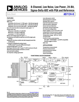
- 1. 8-Channel, Low Noise, Low Power, 24-Bit, Sigma-Delta ADC with PGA and Reference Data Sheet AD7124-8 Rev. B Document Feedback Information furnished by Analog Devices is believed to be accurate and reliable. However, no responsibilityisassumedbyAnalogDevicesforitsuse,norforanyinfringementsofpatentsorother rightsofthirdpartiesthatmayresultfromitsuse.Specificationssubjecttochangewithoutnotice.No licenseisgrantedbyimplicationor otherwiseunderanypatentorpatentrightsofAnalogDevices. Trademarksandregisteredtrademarksarethepropertyoftheirrespectiveowners. One Technology Way, P.O. Box 9106, Norwood, MA 02062-9106, U.S.A. Tel: 781.329.4700 ©2015 Analog Devices, Inc. All rights reserved. Technical Support www.analog.com FEATURES 3 power modes RMS noise Low power: 24 nV rms at 1.17 SPS, gain =128 (255 µA typical) Mid power: 20 nV rms at 2.34 SPS, gain=128 (355 µA typical) Full power: 23 nV rms at 9.4 SPS, gain= 128 (930 µA typical) Up to 22 noise free bits in all power modes (gain = 1) Output data rate Full power: 9.38 SPS to 19,200 SPS Mid power: 2.34 SPS to 4800 SPS Low power: 1.17 SPS to 2400 SPS Rail-to-rail analog inputs for gains > 1 Simultaneous 50 Hz/60 Hzrejectionat 25 SPS (single cycle settling) Diagnostic functions (which aid safe integrity level (SIL) certification) Crosspoint multiplexed analog inputs 8 differential/15 pseudo differential inputs Programmable gain (1 to 128) Band gap reference with 15 ppm/°C drift maximum (65 µA) Matched programmable excitation currents Internal clock oscillator On-chip bias voltage generator Low-side power switch General-purpose outputs Multiple filter options Internal temperature sensor Self and system calibration Sensor burnout detection Automatic channel sequencer Per channel configuration Power supply: 2.7 V to 3.6 V and ±1.8 V Independent interface power supply Power-down current: 5 µA maximum Temperature range: −40°C to +105°C 32-lead LFCSP 3-wire or 4-wire serial interface SPI, QSPI™, MICROWIRE™, and DSP compatible Schmitt trigger on SCLK ESD: 4 kV APPLICATIONS Temperature measurement Pressure measurement Industrial process control Instrumentation Smart transmitters FUNCTIONAL BLOCK DIAGRAM TEMPERATURE SENSOR BANDGAP REF VBIAS SERIAL INTERFACE AND CONTROL LOGIC INTERNAL CLOCK CLK SCLK DIN SYNC REGCAPDIOVDD AD7124-8 AVSS DGND 24-BIT Σ-Δ ADC X-MUX REFIN1(+) AVDD AVSS REFOUT AVDD AVSS PSW VARIABLE DIGITAL FILTER DIAGNOSTICS COMMUNICATIONS POWER SUPPLY SIGNAL CHAIN DIGITAL REFIN1(–) REFIN2(+) REFIN2(–) BURNOUT DETECT EXCITATION CURRENTSPOWER SWITCH GPOs CHANNEL SEQUENCER CROSSPOINT MUX REGCAPAAVDD 1.9V LDO DIAGNOSTICS AVDD AVSS AVSS DOUT/RDY CS 1.8V LDO AIN0/IOUT/VBIAS ANALOG BUFFERS REFERENCE BUFFERS AIN1/IOUT/VBIAS AIN2/IOUT/VBIAS/P1 AIN3/IOUT/VBIAS/P2 AIN4/IOUT/VBIAS/P3 AIN5/IOUT/VBIAS/P4 AIN6/IOUT/VBIAS AIN7/IOUT/VBIAS AIN8/IOUT/VBIAS AIN9/IOUT/VBIAS AIN10/IOUT/VBIAS AIN11/IOUT/VBIAS AIN12/IOUT/VBIAS AIN13/IOUT/VBIAS AIN14/IOUT/VBIAS/REFIN2(+) AIN15/IOUT/VBIAS/REFIN2(–) BUF BUF PGA2PGA1 13048-001 Figure 1.
- 2. AD7124-8 Data Sheet Rev. B | Page 2 of 91 TABLE OF CONTENTS Features .............................................................................................. 1 Applications....................................................................................... 1 Functional Block Diagram .............................................................. 1 Revision History ............................................................................... 3 General Description......................................................................... 4 Specifications..................................................................................... 5 Timing Characteristics .............................................................. 10 Absolute Maximum Ratings.......................................................... 13 Thermal Resistance.................................................................... 13 ESD Caution................................................................................ 13 Pin Configuration and Function Descriptions........................... 14 Terminology.................................................................................... 17 Typical Performance Characteristics ........................................... 18 RMS Noise and Resolution............................................................ 27 Full Power Mode......................................................................... 27 Mid Power Mode........................................................................ 30 Low Power Mode........................................................................ 33 Getting Started................................................................................ 36 Overview...................................................................................... 36 Power Supplies............................................................................ 37 Digital Communication............................................................. 37 Configuration Overview ........................................................... 39 ADC Circuit Information.............................................................. 44 Analog Input Channel ............................................................... 44 Programmable Gain Array (PGA)........................................... 45 Reference ..................................................................................... 45 Bipolar/Unipolar Configuration .............................................. 46 Data Output Coding .................................................................. 46 Excitation Currents .................................................................... 46 Bridge Power-Down Switch...................................................... 46 Logic Outputs.............................................................................. 47 Bias Voltage Generator .............................................................. 47 Clock ............................................................................................ 47 Power Modes............................................................................... 47 Standby and Power-Down Modes............................................ 48 Digital Interface.......................................................................... 48 DATA_STATUS.......................................................................... 50 Serial Interface Reset (DOUT_RDY_DEL and CS_EN Bits)50 Reset .............................................................................................50 Calibration................................................................................... 51 Span and Offset Limits .............................................................. 52 System Synchronization ............................................................ 52 Digital Filter .................................................................................... 53 Sinc4 Filter ................................................................................... 53 Sinc3 Filter ................................................................................... 55 Fast Settling Mode (Sinc4 + Sinc1 Filter).................................. 57 Fast Settling Mode (Sinc3 + Sinc1 Filter).................................. 59 Post Filters................................................................................... 61 Summary of Filter Options ....................................................... 64 Diagnostics...................................................................................... 65 Signal Chain Check.................................................................... 65 Reference Detect......................................................................... 65 Calibration, Conversion, and Saturation Errors .................... 65 Overvoltage/Undervoltage Detection ..................................... 65 Power Supply Monitors ............................................................. 66 LDO Monitoring ........................................................................ 66 MCLK Counter........................................................................... 66 SPI SCLK Counter...................................................................... 66 SPI Read/Write Errors ............................................................... 67 SPI_IGNORE Error ................................................................... 67 Checksum Protection ................................................................ 67 Memory Map Checksum Protection ....................................... 67 Burnout Currents ....................................................................... 69 Temperature Sensor ................................................................... 69 Grounding and Layout .................................................................. 70 Applications Information.............................................................. 71 Temperature Measurement Using a Thermocouple.............. 71 Temperature Measurement Using an RTD............................. 72 Flowmeter.................................................................................... 74 On-Chip Registers.......................................................................... 76 Communications Register......................................................... 77 Status Register............................................................................. 77 ADC_CONTROL Register ....................................................... 78 Data Register............................................................................... 80 IO_CONTROL_1 Register........................................................ 80 IO_CONTROL_2 Register........................................................ 82 ID Register................................................................................... 83 Error Register.............................................................................. 83 ERROR_EN Register ................................................................. 84 MCLK_COUNT Register.......................................................... 85
- 3. Data Sheet AD7124-8 Rev. B | Page 3 of 91 Channel Registers........................................................................86 Configuration Registers .............................................................88 Filter Registers.............................................................................89 Offset Registers............................................................................90 Gain Registers..............................................................................90 Outline Dimensions........................................................................91 Ordering Guide...........................................................................91 REVISION HISTORY 7/15—Rev. A to Rev. B Changes to Figure 29 ......................................................................21 Change to Single Conversion Mode Section ...............................49 Changes to Calibration Section.....................................................51 Changes to Figure 82 ......................................................................53 Changes to Figure 90 ......................................................................56 Changes to Figure 98 ......................................................................58 Changes to Figure 104 ....................................................................60 Changes to Reference Detect Section and Figure 118................65 Changes to Table 70 ........................................................................83 Changes to Table 71................................................................................. 84 Changes to Table 75 ........................................................................89 5/15—Rev. 0 to Rev. A Changes to Temperature Measurement Using a Thermocouple Section ..............................................................................................71 Changed AINM to AINP, Table 70...............................................83 Changed REFOUT to Internal Reference, Table 73 ...................86 4/15—Revision 0: Initial Version
- 4. AD7124-8 Data Sheet Rev. B | Page 4 of 91 GENERAL DESCRIPTION The AD7124-8 is a low power, low noise, completely integrated analog front end for high precision measurement applications. The device contains a low noise, 24-bit Σ-Δ analog-to-digital converter (ADC), and can be configured to have 8 differential inputs or 15 single-ended or pseudo differential inputs. The on- chip low gain stage ensures that signals of small amplitude can be interfaced directly to the ADC. One of the major advantages of the AD7124-8 is that it gives the user the flexibility to employ one of three integrated power modes. The current consumption, range of output data rates, and rms noise can be tailored with the power mode selected. The device also offers a multitude of filter options, ensuring that the user has the highest degree of flexibility. The AD7124-8 can achieve simultaneous 50 Hz and 60 Hz rejection when operating at an output data rate of 25 SPS (single cycle settling), with rejection in excess of 80 dB achieved at lower output data rates. The AD7124-8 establishes the highest degree of signal chain integration. The device contains a precision, low noise, low drift internal band gap reference and accepts an external differential reference, which can be internally buffered. Other key integrated features include programmable low drift excitation current sources, burnout currents, and a bias voltage generator, which sets the common-mode voltage of a channel to AVDD/2. The low-side power switch enables the user to power down bridge sensors between conversions, ensuring the absolute minimal power consumption of the system. The device also allows the user the option of operating with either an internal clock or an external clock. The integrated channel sequencer allows several channels to be enabled simultaneously, and the AD7124-8 sequentially converts on each enabled channel, simplifying communication with the device. As many as 16 channels can be enabled at any time, a channel being defined as an analog input or a diagnostic such as a power supply check or a reference check. This unique feature allows diagnostics to be interleaved with conversions. The AD7124-8 also supports per channel configuration. The device allows eight configurations or setups. Each configuration consists of gain, filter type, output data rate, buffering, and reference source. The user can assign any of these setups on a channel by channel basis. The AD7124-8 also has extensive diagnostic functionality integrated as part of its comprehensive feature set. These diagnostics include a cyclic redundancy check (CRC), signal chain checks, and serial interface checks, which lead to a more robust solution. These diagnostics reduce the need for external components to implement diagnostics, resulting in reduced board space needs, reduced design cycle times, and cost savings. The failure modes effects and diagnostic analysis (FMEDA) of a typical application has shown a safe failure fraction (SFF) greater than 90% according to IEC 61508. The device operates with a single analog power supply from 2.7 V to 3.6 V or a dual 1.8 V power supply. The digital supply has a range of 1.65 V to 3.6 V. It is specified for a temperature range of −40°C to +105°C. The AD7124-8 is housed in a 32-lead LFCSP package. Note that, throughout this data sheet, multifunction pins, such as DOUT/RDY, are referred to either by the entire pin name or by a single function of the pin, for example, RDY, when only that function is relevant. Table 1. AD7124-8 Overview Parameter Low Power Mode Mid Power Mode Full Power Mode Maximum Output Data Rate 2400 SPS 4800 SPS 19,200 SPS RMS Noise (Gain = 128) 24 nV 20 nV 23 nV Peak-to-Peak Resolution at 1200 SPS (Gain = 1) 16.4 bits 17.1 bits 18 bits Typical Current (ADC + PGA) 255 µA 355 µA 930 µA
- 5. Data Sheet AD7124-8 Rev. B | Page 5 of 91 SPECIFICATIONS AVDD = 2.9 V to 3.6 V (full power mode), 2.7 V to 3.6 V (mid and low power mode), IOVDD = 1.65 V to 3.6 V, AVSS = DGND = 0 V, REFINx(+) = 2.5 V, REFINx(−) = AVSS, all specifications TMIN to TMAX, unless otherwise noted. Table 2. Parameter1 Min Typ Max Unit Test Conditions/Comments ADC Output Data Rate, fADC Low Power Mode 1.17 2400 SPS Mid Power Mode 2.34 4800 SPS Full Power Mode 9.38 19,200 SPS No Missing Codes2 24 Bits FS3 > 2, sinc4 filter 24 Bits FS3 > 8, sinc3 filter Resolution See the RMS Noise and Resolution section RMS Noise and Update Rates See the RMS Noise and Resolution section Integral Nonlinearity (INL) Low Power Mode2 −4 ±1 +4 ppm of FSR Gain = 1 −15 ±2 +15 ppm of FSR Gain > 1, TA = −40°C to +85°C −20 ±2 +20 ppm of FSR Gain > 1, TA = −40°C to +105°C Mid Power Mode2 −4 ±1 +4 ppm of FSR Gain = 1 −15 ±2 +15 ppm of FSR Gain > 1 Full Power Mode −4 ±1 +4 ppm of FSR Gain = 12 −15 ±2 +15 ppm of FSR Gain > 1 Offset Error4 Before Calibration ±15 µV Gain = 1 to 8 200/gain µV Gain = 16 to 128 After Internal Calibration/System Calibration In order of noise Offset Error Drift vs. Temperature5 Low Power Mode 10 nV/°C Gain = 1 or gain > 16 80 nV/°C Gain = 2 to 8 40 nV/°C Gain = 16 Mid Power Mode 10 nV/°C Gain = 1 or gain > 16 40 nV/°C Gain = 2 to 8 20 nV/°C Gain = 16 Full Power Mode 10 nV/°C Gain Error4, 6 Before Internal Calibration −0.0025 +0.0025 % Gain = 1, TA = 25°C −0.3 % Gain > 1 After Internal Calibration −0.016 +0.004 +0.016 % Gain = 2 to 8, TA = 25°C ±0.025 % Gain = 16 to 128 After System Calibration In order of noise Gain Error Drift vs. Temperature 1 2 ppm/°C Power Supply Rejection AIN = 1 V/gain, external reference Low Power Mode 84 dB Gain = 2 to 16 91 dB Gain = 1 or gain > 16 Mid Power Mode2 89 dB Gain = 2 to 16 95 dB Gain = 1 or gain > 16 Full Power Mode 96 dB
- 6. AD7124-8 Data Sheet Rev. B | Page 6 of 91 Parameter1 Min Typ Max Unit Test Conditions/Comments Common-Mode Rejection7 At DC2 85 90 dB AIN = 1 V, gain = 1 At DC 100 105 dB AIN = 1 V/gain, gain 2 or 4 110 115 dB AIN = 1 V/gain, gain ≥ 8 Sinc3 , Sinc4 Filter2 At 50 Hz, 60 Hz 120 dB 10 SPS, 50 Hz ± 1 Hz, 60 Hz ± 1 Hz At 50 Hz 120 dB 50 SPS, 50 Hz ± 1 Hz At 60 Hz 120 dB 60 SPS, 60 Hz ± 1 Hz Fast Settling Filters2 At 50 Hz 115 dB First notch at 50 Hz, 50 Hz ± 1 Hz At 60 Hz 115 dB First notch at 60 Hz, 60 Hz ± 1 Hz Post Filters2 At 50 Hz, 60 Hz 130 dB 20 SPS, 50 Hz ± 1 Hz, 60 Hz ± 1 Hz 130 dB 25 SPS, 50 Hz ± 1 Hz, 60 Hz ± 1 Hz Normal Mode Rejection2 Sinc4 Filter External Clock At 50 Hz, 60 Hz 120 dB 10 SPS, 50 Hz ± 1 Hz, 60 Hz ± 1 Hz 82 dB 50 SPS, REJ608 =1, 50 Hz ± 1 Hz, 60 Hz ± 1 Hz At 50 Hz 120 dB 50 SPS, 50 Hz ± 1 Hz At 60 Hz 120 dB 60 SPS, 60 Hz ± 1 Hz Internal Clock At 50 Hz, 60 Hz 98 dB 10 SPS, 50 Hz ± 1 Hz, 60 Hz ± 1 Hz 66 dB 50 SPS, REJ608 = 1, 50 Hz ± 1 Hz, 60 Hz ± 1 Hz At 50 Hz 92 dB 50 SPS, 50 Hz ± 1 Hz At 60 Hz 92 dB 60 SPS, 60 Hz ± 1 Hz Sinc3 Filter External Clock At 50 Hz, 60 Hz 100 dB 10 SPS, 50 Hz ± 1 Hz, 60 Hz ± 1 Hz 66 dB 50 SPS, REJ608 = 1, 50 Hz ± 1 Hz, 60 Hz ± 1 Hz At 50 Hz 100 dB 50 SPS, 50 Hz ± 1 Hz At 60 Hz 100 dB 60 SPS, 60 Hz ± 1 Hz Internal Clock At 50 Hz, 60 Hz 73 dB 10 SPS, 50 Hz ± 1 Hz, 60 Hz ± 1 Hz 52 dB 50 SPS, REJ608 = 1, 50 Hz ± 1 Hz, 60 Hz ± 1 Hz At 50 Hz 68 dB 50 SPS, 50 Hz ± 1 Hz At 60 Hz 68 dB 60 SPS, 60 Hz ± 1 Hz Fast Settling Filters External Clock At 50 Hz 40 dB First notch at 50 Hz, 50 Hz ± 0.5 Hz At 60 Hz 40 dB First notch at 60 Hz, 60 Hz ± 0.5 Hz Internal Clock At 50 Hz 24.5 dB First notch at 50 Hz, 50 Hz ± 0.5 Hz At 60 Hz 24.5 dB First notch at 60 Hz, 60 Hz ± 0.5 Hz Post Filters External Clock At 50 Hz, 60 Hz 86 dB 20 SPS, 50 Hz ± 1 Hz, 60 Hz ± 1 Hz 62 dB 25 SPS, 50 Hz ± 1 Hz, 60 Hz ± 1 Hz Internal Clock At 50 Hz, 60 Hz 67 dB 20 SPS, 50 Hz ± 1 Hz, 60 Hz ± 1 Hz 50 dB 25 SPS, 50 Hz ± 1 Hz, 60 Hz ± 1 Hz
- 7. Data Sheet AD7124-8 Rev. B | Page 7 of 91 Parameter1 Min Typ Max Unit Test Conditions/Comments ANALOG INPUTS9 Differential Input Voltage Ranges10 ±VREF/gain V VREF = REFINx(+) − REFINx(−), or internal reference Absolute AIN Voltage Limits2 Gain = 1 (Unbuffered) AVSS − 0.05 AVDD + 0.05 V Gain = 1 (Buffered) AVSS + 0.1 AVDD − 0.1 V Gain > 1 AVSS − 0.05 AVDD + 0.05 V Analog Input Current Gain > 1 or Gain = 1 (Buffered) Low Power Mode Absolute Input Current ±1 nA Differential Input Current ±0.2 nA Analog Input Current Drift 25 pA/°C Mid Power Mode Absolute Input Current ±1.2 nA Differential Input Current ±0.4 nA Analog Input Current Drift 25 pA/°C Full Power Mode Absolute Input Current ±3.3 nA Differential Input Current ±1.5 nA Analog Input Current Drift 25 pA/°C Gain = 1 (Unbuffered) Current varies with input voltage Absolute Input Current ±2.65 µA/V Analog Input Current Drift 1.1 nA/V/°C REFERENCE INPUT Internal Reference Initial Accuracy 2.5 − 0.2% 2.5 2.5 + 0.2% V TA = 25°C Drift 2 8 ppm/°C TA = 25°C to 105°C 2 15 ppm/°C TA = −40°C to +105°C Output Current 10 mA Load Regulation 50 µV/mA Power Supply Rejection 85 dB External Reference External REFIN Voltage2 1 2.5 AVDD V REFIN = REFINx(+) − REFINx(−) Absolute REFIN Voltage Limits2 AVSS − 0.05 AVDD + 0.05 V Unbuffered AVSS + 0.1 AVDD − 0.1 V Buffered Reference Input Current Buffered Low Power Mode Absolute Input Current ±0.5 nA Reference Input Current Drift 10 pA/°C Mid Power Mode Absolute Input Current ±1 nA Reference Input Current Drift 10 pA/°C Full Power Mode Absolute Input Current ±3 nA Reference Input Current Drift 10 pA/°C Unbuffered Absolute Input Current ±12 µA Reference Input Current Drift 6 nA/°C Normal Mode Rejection Same as for analog inputs Common-Mode Rejection 100 dB
- 8. AD7124-8 Data Sheet Rev. B | Page 8 of 91 Parameter1 Min Typ Max Unit Test Conditions/Comments EXCITATION CURRENT SOURCES (IOUT0/IOUT1) Available on any analog input pin Output Current 50/100/250/ 500/750/1000 µA Initial Tolerance ±4 % TA = 25°C Drift 50 ppm/°C Current Matching ±0.5 % Matching between IOUT0 and IOUT1, VOUT = 0 V Drift Matching 5 30 ppm/°C Line Regulation (AVDD) 2 %/V AVDD = 3 V ± 5% Load Regulation 0.2 %/V Output Compliance2 AVSS − 0.05 AVDD − 0.37 V 50 µA/100 µA/250 µA/500 µA current sources, 2% accuracy AVSS − 0.05 AVDD − 0.48 V 750 µA and 1000 µA current sources, 2% accuracy BIAS VOLTAGE (VBIAS) GENERATOR Available on any analog input pin VBIAS AVSS + (AVDD − AVSS)/2 V VBIAS Generator Start-Up Time 6.7 µs/nF Dependent on the capacitance connected to AIN TEMPERATURE SENSOR Accuracy ±0.5 °C Sensitivity 13,584 codes/°C LOW-SIDE POWER SWITCH On Resistance (RON) 7 10 Ω Allowable Current2 30 mA Continuous current BURNOUT CURRENTS AIN Current 0.5/2/4 µA Analog inputs must be buffered DIGITAL OUTPUTS (P1 to P4) Output Voltage High, VOH AVDD − 0.6 V ISOURCE = 100 µA Low, VOL 0.4 V ISINK = 100 µA DIAGNOSTICS Power Supply Monitor Detect Level Analog Low Dropout Regulator (ALDO) 1.6 V AVDD − AVSS ≥ 2.7 V Digital LDO (DLDO) 1.55 V IOVDD ≥ 1.75 V Reference Detect Level 0.7 1 V REF_DET_ERR bit active if VREF < 0.7V AINM/AINP Overvoltage Detect Level AVDD + 0.04 V AINM/AINP Undervoltage Detect Level AVSS − 0.04 V INTERNAL/EXTERNAL CLOCK Internal Clock Frequency 614.4 − 5% 614.4 614.4 + 5% kHz Duty Cycle 50:50 % External Clock Frequency 2.4576 MHz Internal divide by 4 Duty Cycle Range 45:55 to 55:45 % LOGIC INPUTS2 Input Voltage Low, VINL 0.3 × IOVDD V 1.65 V ≤ IOVDD < 1.9 V 0.35 × IOVDD V 1.9 V ≤ IOVDD < 2.3 V 0.7 V 2.3 V ≤ IOVDD ≤ 3.6 V High, VINH 0.7 × IOVDD V 1.65 V ≤ IOVDD < 1.9 V 0.65 × IOVDD V 1.9 V ≤ IOVDD < 2.3 V 1.7 V 2.3 V ≤ IOVDD < 2.7 V 2 V 2.7 V ≤ IOVDD ≤ 3.6 V Hysteresis 0.2 0.6 V 1.65 V ≤ IOVDD ≤ 3.6 V Input Currents −1 +1 µA VIN = IOVDD or GND Input Capacitance 10 pF All digital inputs
- 9. Data Sheet AD7124-8 Rev. B | Page 9 of 91 Parameter1 Min Typ Max Unit Test Conditions/Comments LOGIC OUTPUTS (INCLUDING CLK) Output Voltage2 High, VOH IOVDD − 0.35 V ISOURCE = 100 µA Low, VOL 0.4 V ISINK = 100 µA Floating State Leakage Current −1 +1 µA Floating State Output Capacitance 10 pF Data Output Coding Offset binary SYSTEM CALIBRATION2 Calibration Limit Full-Scale 1.05 × FS V Zero-Scale −1.05 × FS V Input Span 0.8 × FS 2.1 × FS V POWER SUPPLY VOLTAGES FOR ALL POWER MODES AVDD to AVSS Low Power Mode 2.7 3.6 V Mid Power Mode 2.7 3.6 V Full Power Mode 2.9 3.6 V IOVDD to GND 1.65 3.6 V AVSS to GND −1.8 0 +1.8 V IOVDD to AVSS 5.4 V POWER SUPPLY CURRENTS9, 11 IAVDD, External Reference Low Power Mode Gain = 12 125 135 µA All buffers off Gain = 1 IAVDD Increase per AIN Buffer2 15 20 µA Gain = 2 to 8 205 235 µA Gain = 16 to 128 235 280 µA IAVDD Increase per Reference Buffer2 10 15 µA All gains Mid Power Mode Gain = 12 150 165 µA All buffers off Gain = 1 IAVDD Increase per AIN Buffer2 30 35 µA Gain = 2 to 8 275 325 µA Gain = 16 to 128 330 405 µA IAVDD Increase per Reference Buffer2 20 30 µA All gains Full Power Mode Gain = 12 315 345 µA All buffers off Gain = 1 IAVDD Increase per AIN Buffer2 90 125 µA Gain = 2 to 8 660 790 µA Gain = 16 to 128 875 1100 µA IAVDD Increase per Reference Buffer2 85 110 µA All gains IAVDD Increase Due to Internal Reference2 50 65 µA Independent of power mode; the reference buffers are not required when using this reference Due to VBIAS 2 15 20 µA Independent of power mode Due to Diagnostics2 4 5 µA IIOVDD Low Power Mode 20 35 µA Mid Power Mode 25 40 µA Full Power Mode 55 85 µA
- 10. AD7124-8 Data Sheet Rev. B | Page 10 of 91 Parameter1 Min Typ Max Unit Test Conditions/Comments POWER-DOWN CURRENTS11 Independent of power mode Standby Current IAVDD 7 12 µA LDOs on only IIOVDD 8 17 µA Power-Down Current IAVDD 1 3 µA IIOVDD 1 2 µA 1 Temperature range = −40°C to +105°C. 2 These specifications are not production tested but are supported by characterization data at the initial product release. 3 FS is the decimal equivalent of the FS[10:0] bits in the filter registers. 4 Following a system or internal zero-scale calibration, the offset error is in the order of the noise for the programmed gain and output data rate selected. A system full- scale calibration reduces the gain error to the order of the noise for the programmed gain and output data rate. 5 Recalibration at any temperature removes these errors. 6 Gain error applies to both positive and negative full-scale. A factory calibration is performed at gain = 1, TA = 25°C. 7 When gain > 1, the common-mode voltage is between (AVSS + 0.1 + 0.1/gain) and (AVDD − 0.1 − 0.5/gain). 8 REJ60 is a bit in the filter registers. When the first notch of the sinc filter is at 50 Hz, a notch is placed at 60 Hz when REJ60 is set to 1. This gives simultaneous 50 Hz and 60 Hz rejection. 9 When the gain is greater than 1, the analog input buffers are enabled automatically. The buffers can only be disabled when the gain equals 1. 10 When VREF = (AVDD − AVSS), the typical differential input equals 0.92 × VREF/gain for the low and mid power modes and 0.86 × VREF/gain for full power mode. 11 The digital inputs are equal to IOVDD or DGND with excitation currents and bias voltage generator disabled. TIMING CHARACTERISTICS AVDD = 2.9 V to 3.6 V (full power mode), 2.7 V to 3.6 V (mid and low power mode), IOVDD = 1.65 V to 3.6 V, AVSS = DGND = 0 V, Input Logic 0 = 0 V, Input Logic 1 = IOVDD, unless otherwise noted. Table 3. Parameter1, 2 Min Typ Max Unit Test Conditions/Comments t3 100 ns SCLK high pulse width t4 100 ns SCLK low pulse width t12 Delay between consecutive read/write operations 3/MCLK3 ns Full power mode 12/MCLK ns Mid power mode 24/MCLK ns Low power mode t13 µs DOUT/RDY high time if DOUT/RDY is low and the next conversion is available 6 µs Full power mode 25 µs Mid power mode 50 µs Low power mode t14 SYNC low pulse width 3/MCLK ns Full power mode 12/MCLK ns Mid power mode 24/MCLK ns Low power mode READ OPERATION t1 0 80 ns CS falling edge to DOUT/RDY active time t2 4 0 80 ns SCLK active edge5 to data valid delay t5 6, 7 10 80 ns Bus relinquish time after CS inactive edge t6 0 ns SCLK inactive edge to CS inactive edge t7 8 SCLK inactive edge to DOUT/RDY high 10 ns The DOUT_RDY_DEL bit is cleared, the CS_EN bit is cleared 110 ns The DOUT_RDY_DEL bit is set, the CS_EN bit is cleared t7A 7 t5 ns Data valid after CS inactive edge, the CS_EN bit is set
- 11. Data Sheet AD7124-8 Rev. B | Page 11 of 91 Parameter1, 2 Min Typ Max Unit Test Conditions/Comments WRITE OPERATION t8 0 ns CS falling edge to SCLK active edge5 setup time t9 30 ns Data valid to SCLK edge setup time t10 25 ns Data valid to SCLK edge hold time t11 0 ns CS rising edge to SCLK edge hold time 1 These specifications were sample tested during the initial release to ensure compliance. All input signals are specified with tR = tF = 5 ns (10% to 90% of IOVDD and timed from a voltage level of IOVDD/2. 2 See Figure 3, Figure 4, Figure 5, and Figure 6. 3 MCLK is the master clock frequency. 4 These specifications are measured with the load circuit shown in Figure 2 and defined as the time required for the output to cross the VOL or VOH limits. 5 The SCLK active edge is the falling edge of SCLK. 6 These specifications are derived from the measured time taken by the data output to change by 0.5 V when loaded with the circuit shown in Figure 2. The measured number is then extrapolated back to remove the effects of charging or discharging the 25 pF capacitor. The times quoted in the timing characteristics are the true bus relinquish times of the device and, therefore, are independent of external bus loading capacitances. 7 RDY returns high after a read of the ADC. In single conversion mode and continuous conversion mode, the same data can be read again, if required, while RDY is high, although subsequent reads must not occur close to the next output update. In continuous read mode, the digital word can be read only once. 8 When the CS_EN bit is cleared, the DOUT/RDY pin changes from its DOUT function to its RDY function, following the last inactive edge of the SCLK. When CS_EN is set, the DOUT pin continues to output the LSB of the data until the CS inactive edge. Timing Diagrams IOVDD/2TO OUTPUT PIN ISOURCE (100µA) ISINK (100µA) 25pF 13048-002 Figure 2. Load Circuit for Timing Characterization t3 t2 t7 t6 t5 t4 t1 MSB LSBDOUT/RDY (O) SCLK (I) CS (I) I = INPUT, O = OUTPUT 13048-003 Figure 3. Read Cycle Timing Diagram (CS_EN Bit Cleared)
- 12. AD7124-8 Data Sheet Rev. B | Page 12 of 91 t5 t3 t2 t4 t1 MSBDOUT/RDY (O) SCLK (I) CS (I) I = INPUT, O = OUTPUT LSB t7A t6 13048-004 Figure 4. Read Cycle Timing Diagram (CS_EN Bit Set) CS (I) SCLK (I) DIN (I) MSB LSB t8 t9 t10 t11 I = INPUT, O = OUTPUT 13048-005 Figure 5. Write Cycle Timing Diagram WRITEDIN DOUT/RDY SCLK WRITE t12 t12 t12 READREAD 13048-006 Figure 6. Delay Between Consecutive Serial Operations DIN DOUT/RDY CS SCLK t13 13048-007 Figure 7. DOUT/RDY High Time when DOUT/RDY is Initially Low and the Next Conversion is Available SYNC (I) MCLK (I) t14 13048-008 Figure 8. SYNC Pulse Width
- 13. Data Sheet AD7124-8 Rev. B | Page 13 of 91 ABSOLUTE MAXIMUM RATINGS TA = 25°C, unless otherwise noted. Table 4. Parameter Rating AVDD to AVSS −0.3 V to +3.96 V IOVDD to DGND −0.3 V to +3.96 V IOVDD to DGND −0.3 V to +3.96 V IOVDD to AVSS −0.3 V to +5.94 V AVSS to DGND −1.98 V to +0.3 V Analog Input Voltage to AVSS −0.3 V to AVDD + 0.3 V Reference Input Voltage to AVSS −0.3 V to AVDD + 0.3 V Digital Input Voltage to DGND −0.3 V to IOVDD + 0.3 V Digital Output Voltage to DGND −0.3 V to IOVDD + 0.3 V AINx/Digital Input Current 10 mA Operating Temperature Range −40°C to +105°C Storage Temperature Range −65°C to +150°C Maximum Junction Temperature 150°C Lead Temperature, Soldering Reflow 260°C ESD Ratings Human Body Model (HBM) 4 kV Field-Induced Charged Device Model (FICDM) 1250 V Machine Model 400 V Stresses at or above those listed under Absolute Maximum Ratings may cause permanent damage to the product. This is a stress rating only; functional operation of the product at these or any other conditions above those indicated in the operational section of this specification is not implied. Operation beyond the maximum operating conditions for extended periods may affect product reliability. THERMAL RESISTANCE θJA is specified for the worst case conditions, that is, a device soldered in a circuit board for surface-mount packages. Table 5. Thermal Resistance Package Type θJA θJC Unit 32-Lead LFCSP 32.5 32.71 °C/W ESD CAUTION
- 14. AD7124-8 Data Sheet Rev. B | Page 14 of 91 PIN CONFIGURATION AND FUNCTION DESCRIPTIONS NOTES 1. CONNECT EXPOSED PAD TO AVSS. CS REGCAPD AIN5/IOUT/VBIAS/P4 IOVDD DGND AIN0/IOUT/VBIAS AIN1/IOUT/VBIAS AIN2/IOUT/VBIAS/P1 AIN3/IOUT/VBIAS/P2 AIN4/IOUT/VBIAS/P3 REGCAPA AVSS REFOUT AIN15/IOUT/VBIAS/REFIN2(–) AIN14/IOUT/VBIAS/REFIN2(+) AIN13/IOUT/VBIAS AIN12/IOUT/VBIAS AIN11/IOUT/VBIAS CLK SCLK DIN DOUT/RDY SYNC AVDD PSW AIN6/IOUT/VBIAS AIN7/IOUT/VBIAS REFIN1(+) REFIN1(–) AIN8/IOUT/VBIAS AIN9/IOUT/VBIAS AIN10/IOUT/VBIAS 24 23 22 21 20 19 18 17 1 2 3 4 5 6 7 8 9 10 11 12 13 14 15 16 32 31 30 29 28 27 26 25 AD7124-8 TOP VIEW (Not to Scale) 13048-009 Figure 9. Pin Configuration Table 6. Pin Function Descriptions PinNo. Mnemonic Description 1 REGCAPD Digital LDO Regulator Output. Decouple this pin to DGND with a 0.1 µF capacitor. 2 IOVDD Serial Interface Supply Voltage, 1.65 V to 3.6 V. IOVDD is independent of AVDD. Therefore, the serial interface can operate at 1.65 V with AVDD at 3.6 V, for example. 3 DGND Digital Ground Reference Point. 4 AIN0/IOUT/VBIAS Analog Input 0/Output of Internal Excitation Current Source/Bias Voltage. This input pin is configured via the configuration registers to be the positive or negative terminal of a differential or pseudo differential input. Alternatively, the internal programmable excitation current source can be made available at this pin. Either IOUT1 or IOUT0 can be switched to this output. A bias voltage midway between the analog power supply rails can be generated at this pin. 5 AIN1/IOUT/VBIAS Analog Input 1/Output of Internal Excitation Current Source/Bias Voltage. This input pin is configured via the configuration registers to be the positive or negative terminal of a differential or pseudo differential input. Alternatively, the internal programmable excitation current source can be made available at this pin. Either IOUT0 or IOUT1 can be switched to this output. A bias voltage midway between the analog power supply rails can be generated at this pin. 6 AIN2/IOUT/VBIAS/P1 Analog Input 2/Output of Internal Excitation Current Source/Bias Voltage/General-Purpose Output 1. This input pin is configured via the configuration registers to be the positive or negative terminal of a differential or pseudo differential input. Alternatively, the internal programmable excitation current source can be made available at this pin. Either IOUT0 or IOUT1 can be switched to this output. A bias voltage midway between the analog power supply rails can be generated at this pin. This pin can also be configured as a general-purpose output bit, referenced between AVSS and AVDD. 7 AIN3/IOUT/VBIAS/P2 Analog Input 3/Output of Internal Excitation Current Source/Bias Voltage/General-Purpose Output 2. This input pin is configured via the configuration registers to be the positive or negative terminal of a differential or pseudo differential input. Alternatively, the internal programmable excitation current source can be made available at this pin. Either IOUT0 or IOUT1 can be switched to this output. A bias voltage midway between the analog power supply rails can be generated at this pin. This pin can also be configured as a general-purpose output bit, referenced between AVSS and AVDD. 8 AIN4/IOUT/VBIAS/P3 Analog Input 4/Output of Internal Excitation Current Source/Bias Voltage/General-Purpose Output 3. This input pin is configured via the configuration registers to be the positive or negative terminal of a differential or pseudo differential input. Alternatively, the internal programmable excitation current source can be made available at this pin. Either IOUT0 or IOUT1 can be switched to this output. A bias voltage midway between the analog power supply rails can be generated at this pin. This pin can also be configured as a general-purpose output bit, referenced between AVSS and AVDD.
- 15. Data Sheet AD7124-8 Rev. B | Page 15 of 91 PinNo. Mnemonic Description 9 AIN5/IOUT/VBIAS/P4 Analog Input 5/Output of Internal Excitation Current Source/Bias Voltage/General-Purpose Output 4. This input pin is configured via the configuration registers to be the positive or negative terminal of a differential or pseudo differential input. Alternatively, the internal programmable excitation current source can be made available at this pin. Either IOUT0 or IOUT1 can be switched to this output. A bias voltage midway between the analog power supply rails can be generated at this pin. This pin can also be configured as a general-purpose output bit, referenced between AVSS and AVDD. 10 AIN6/IOUT/VBIAS Analog Input 6/Output of Internal Excitation Current Source/Bias Voltage. This input pin is configured via the configuration registers to be the positive or negative terminal of a differential or pseudo differential input. Alternatively, the internal programmable excitation current source can be made available at this pin. Either IOUT0 or IOUT1 can be switched to this output. A bias voltage midway between the analog power supply rails can be generated at this pin. 11 AIN7/IOUT/VBIAS Analog Input 7/Output of Internal Excitation Current Source/Bias Voltage. This input pin is configured via the configuration registers to be the positive or negative terminal of a differential or pseudo differential input. Alternatively, the internal programmable excitation current source can be made available at this pin. Either IOUT0 or IOUT1 can be switched to this output. A bias voltage midway between the analog power supply rails can be generated at this pin. 12 REFIN1(+) Positive Reference Input. An external reference can be applied between REFIN1(+) and REFIN1(−). REFIN1(+) can be anywhere between AVDD and AVSS + 1 V. The nominal reference voltage (REFIN1(+) − REFIN1(−)) is 2.5 V, but the device functions with a reference from 1 V to AVDD. 13 REFIN1(−) Negative Reference Input. This reference input can be anywhere between AVSS and AVDD − 1 V. 14 AIN8/IOUT/VBIAS Analog Input 8/Output of Internal Excitation Current Source/BiasVoltage.This input pin is configured via the configuration registers to be the positive or negative terminal of a differential or pseudo differential input. Alternatively, the internal programmable excitation current source can be made available at this pin. Either IOUT0 or IOUT1 can be switched to this output. A bias voltage midway between the analog power supply rails can be generated at this pin. 15 AIN9/IOUT/VBIAS Analog Input 9/Output of Internal Excitation Current Source/BiasVoltage.This input pin is configured via the configuration registers to be the positive or negative terminal of a differential or pseudo differential input. Alternatively, the internal programmable excitation current source can be made available at this pin. Either IOUT0 or IOUT1 can be switched to this output. A bias voltage midway between the analog power supply rails can be generated at this pin. 16 AIN10/IOUT/VBIAS Analog Input 10/Output of Internal Excitation Current Source/BiasVoltage.This input pin is configured via the configuration registers to be the positive or negative terminal of a differential or pseudo differential input. Alternatively, the internal programmable excitation current source can be made available at this pin. Either IOUT0 or IOUT1 can be switched to this output. A bias voltage midway between the analog power supply rails can be generated at this pin. 17 AIN11/IOUT/VBIAS Analog Input 11/Output of Internal Excitation Current Source/BiasVoltage.This input pin is configured via the configuration registers to be the positive or negative terminal of a differential or pseudo differential input. Alternatively, the internal programmable excitation current source can be made available at this pin. Either IOUT0 or IOUT1 can be switched to this output. A bias voltage midway between the analog power supply rails can be generated at this pin. 18 AIN12/IOUT/VBIAS Analog Input 12/Output of Internal Excitation Current Source/BiasVoltage.This input pin is configured via the configuration registers to be the positive or negative terminal of a differential or pseudo differential input. Alternatively, the internal programmable excitation current source can be made available at this pin. Either IOUT0 or IOUT1 can be switched to this output. A bias voltage midway between the analog power supply rails can be generated at this pin. 19 AIN13/IOUT/VBIAS Analog Input 13/Output of Internal Excitation Current Source/BiasVoltage.This input pin is configured via the configuration registers to be the positive or negative terminal of a differential or pseudo differential input. Alternatively, the internal programmable excitation current source can be made available at this pin. Either IOUT0 or IOUT1 can be switched to this output. A bias voltage midway between the analog power supply rails can be generated at this pin. 20 AIN14/IOUT/VBIAS/ REFIN2(+) Analog Input 14/Output of Internal Excitation Current Source/Bias Voltage/Positive Reference Input. This input pin is configured via the configuration registers to be the positive or negative terminal of a differential or pseudo differential input. Alternatively, the internal programmable excitation current source can be made available at this pin. Either IOUT0 or IOUT1 can be switched to this output. A bias voltage midway between the analog power supply rails can be generated at this pin. This pin also functions as a positive reference input for REFIN2(±). REFIN2(+) can be anywhere between AVDD and AVSS + 1 V. The nominal reference voltage (REFIN2(+) to REFIN2(−)) is 2.5V, but the device functions with a reference from 1V to AVDD.
- 16. AD7124-8 Data Sheet Rev. B | Page 16 of 91 PinNo. Mnemonic Description 21 AIN15/IOUT/VBIAS/ REFIN2(−) Analog Input 15/Output of Internal Excitation Current Source/Bias Voltage/Negative Reference Input. This input pin is configured via the configuration registers to be the positive or negative terminal of a differential or pseudo differential input. Alternatively, the internal programmable excitation current source can be made available at this pin. Either IOUT0 or IOUT1 can be switched to this output. A bias voltage midway between the analog power supply rails can be generated at this pin. This pin also functions as the negative reference input for REFIN2(±).This reference input can be anywhere between AVSS and AVDD − 1V. 22 REFOUT Internal Reference Output.The buffered output of the internal 2.5V voltage reference is available on this pin. 23 AVSS Analog Supply Voltage. The voltage on AVDD is referenced to AVSS. The differential between AVDD and AVSS must be between 2.7 V and 3.6 V in mid or low power mode and between 2.9 V and 3.6 V in full power mode. AVSS can be taken below 0 V to provide a dual power supply to the AD7124-8. For example, AVSS can be tied to −1.8 V and AVDD can be tied to +1.8 V, providing a ±1.8 V supply to the ADC. 24 REGCAPA Analog LDO Regulator Output. Decouple this pin to AVSS with a 0.1 µF capacitor. 25 PSW Low-Side Power Switch to AVSS. 26 AVDD Analog Supply Voltage, Relative to AVSS. 27 SYNC Synchronization Input. This pin is a logic input that allows synchronization of the digital filters and analog modulators when using a number of AD7124-8 devices. When SYNC is low, the nodes of the digital filter, the filter control logic, and the calibration control logic are reset, and the analog modulator is held in a reset state. SYNC does not affect the digital interface but does reset RDY to a high state if it is low. 28 DOUT/RDY Serial Data Output/Data Ready Output. DOUT/RDY functions as a serial data output pin to access the output shift register of the ADC. The output shift register can contain data from any of the on-chip data or control registers. In addition, DOUT/RDY operates as a data ready pin, going low to indicate the completion of a conversion. If the data is not read after the conversion, the pin goes high before the next update occurs. The DOUT/RDY falling edge can also be used as an interrupt to a processor, indicating that valid data is available. With an external serial clock, the data can be read using the DOUT/RDY pin. When CS is low, the data/control word information is placed on the DOUT/RDY pin on the SCLK falling edge and is valid on the SCLK rising edge. 29 DIN Serial Data Input to the Input Shift Register on the ADC. Data in the input shift register is transferred to the control registers within the ADC, with the register selection bits of the communications register identifying the appropriate register. 30 SCLK Serial Clock Input.This serial clock input is for data transfers to and from the ADC.The SCLK pin has a Schmitt- triggered input, making the interface suitable for opto-isolated applications.The serial clock can be continuous with all data transmitted in a continuous train of pulses. Alternatively, it can be a noncontinuous clock with the information being transmitted to or from the ADC in smaller batches of data. 31 CLK Clock Input/Clock Output. The internal clock can be made available at this pin. Alternatively, the internal clock can be disabled, and the ADC can be driven by an external clock. This allows several ADCs to be driven from a common clock, allowing simultaneous conversions to be performed. 32 CS Chip Select Input. This is an active low logic input that selects the ADC. Use CS to select the ADC in systems with more than one device on the serial bus or as a frame synchronization signal in communicating with the device. CS can be hardwired low if the serial peripheral interface (SPI) diagnostics are unused, allowing the ADC to operate in 3-wire mode with SCLK, DIN, and DOUT interfacing with the device. EP Exposed Pad. Connect the exposed pad to AVSS.
- 17. Data Sheet AD7124-8 Rev. B | Page 17 of 91 TERMINOLOGY AINP AINP refers to the positive analog input. AINM AINM refers to the negative analog input. Integral Nonlinearity (INL) INL is the maximum deviation of any code from a straight line passing through the endpoints of the transfer function. The endpoints of the transfer function are zero scale (not to be confused with bipolar zero), a point 0.5 LSB below the first code transition (000 … 000 to 000 … 001), and full scale, a point 0.5 LSB above the last code transition (111 … 110 to 111 … 111). The error is expressed in ppm of the full-scale range. Gain Error Gain error is the deviation of the last code transition (111 … 110 to 111 … 111) from the ideal AINP voltage (AINM + VREF/gain − 3/2 LSBs). Gain error applies to both unipolar and bipolar analog input ranges. Gain error is a measure of the span error of the ADC. It includes full-scale errors but not zero-scale errors. For unipolar input ranges, it is defined as full-scale error minus unipolar offset error; whereas for bipolar input ranges it is defined as full-scale error minus bipolar zero error. Offset Error Offset error is the deviation of the first code transition from the ideal AINP voltage (AINM + 0.5 LSB) when operating in the unipolar mode. In bipolar mode, offset error is the deviation of the midscale transition (0111 … 111 to 1000 … 000) from the ideal AINP voltage (AINM − 0.5 LSB). Offset Calibration Range In the system calibration modes, the AD7124-8 calibrates offset with respect to the analog input. The offset calibration range specification defines the range of voltages that the AD7124-8 can accept and still calibrate offset accurately. Full-Scale Calibration Range The full-scale calibration range is the range of voltages that the AD7124-8 can accept in the system calibration mode and still calibrate full scale correctly. Input Span In system calibration schemes, two voltages applied in sequence to the AD7124-8 analog input define the analog input range. The input span specification defines the minimum and maximum input voltages from zero to full scale that the AD7124-8 can accept and still calibrate gain accurately.
- 18. AD7124-8 Data Sheet Rev. B | Page 18 of 91 TYPICAL PERFORMANCE CHARACTERISTICS 2500 0 500 1000 1500 2000 7FFFCE 7FFFCF 7FFFD0 7FFFD1 7FFFD2 7FFFD3 7FFFD4 7FFFD5 7FFFD6 7FFFD7 7FFFD8 7FFFD9 7FFFDA 7FFFDB 7FFFDC OCCURRENCE CODES (HEX) 10,000 SAMPLES 13048-010 Figure 10. Noise Histogram Plot (Full Power Mode, Post Filter, Output Data Rate = 25 SPS, Gain = 1) 1200 1000 800 600 400 200 0 7FFFC6 7FFFC7 7FFFC8 7FFFC9 7FFFCA 7FFFCB 7FFFCC 7FFFCD 7FFFCE 7FFFCF 7FFFD0 7FFFD1 7FFFD2 7FFFD3 7FFFD4 7FFFD5 7FFFD6 7FFFD7 7FFFD8 7FFFD9 7FFFDA 7FFFDB 7FFFDC 7FFFDE 7FFFDD 7FFFDF 7FFFE0 7FFFE1 7FFFE2 7FFFE3 OCCURRENCE CODES (HEX) 10,000 SAMPLES 13048-012 Figure 11. Noise Histogram Plot (Mid Power Mode, Post Filter, Output Data Rate = 25 SPS, Gain = 1) 700 600 500 400 300 200 100 0 7FFFC1 7FFFC3 7FFFC5 7FFFC7 7FFFC9 7FFFCB 7FFFCD 7FFFCF 7FFFD1 7FFFD3 7FFFD5 7FFFD7 7FFFD9 7FFFDB 7FFFDD 7FFFDF 7FFFE1 7FFFE3 7FFFE5 7FFFE7 7FFFE9 7FFFEB 7FFFED 7FFFF0 7FFFF2 OCCURRENCE CODES (HEX) 10,000 SAMPLES 13048-014 Figure 12. Noise Histogram Plot (Low Power Mode, Post Filter, Output Data Rate = 25 SPS, Gain = 1) 350 300 250 200 150 100 50 0 7FFFE9 7FFFFA 800002 800009 800011 800019 800020 800028 800030 800038 80003F 800047 80004F 800057 80005E 800066 80006E 800075 80007D 800085 80008D 800094 80009C 8000A4 OCCURRENCE CODES (HEX) 10,000 SAMPLES 13048-011 Figure 13. Noise Histogram Plot (Full Power Mode, Post Filter, Output Data Rate = 25 SPS, Gain = 128) 400 350 300 250 200 150 100 50 0 8388394.0 8388452.8 8388469.6 8388486.4 8388503.2 8388520.0 8388536.8 8388553.6 8388570.4 8388587.2 8388604.0 8388620.8 8388637.6 8388654.4 8388671.2 8388688.0 8388704.8 8388721.6 8388738.4 8388755.2 8388772.0 8388788.8 8388805.6 OCCURRENCE CODES (HEX) 10,000 SAMPLES 13048-013 Figure 14. Noise Histogram Plot (Mid Power Mode, Post Filter, Output Data Rate = 25 SPS, Gain = 128) 400 50 100 150 200 250 300 350 0 7FFEED 7FFF03 7FFF1A 7FFF30 7FFF47 7FFF5D 7FFF74 7FFF8A 7FFFA1 7FFFB8 7FFFCE 7FFFFB 7FFFE5 800012 800028 80003F 800055 80006C 800083 800099 8000B0 8000C6 8000F3 80010A 800121 8000DD OCCURRENCE CODES (HEX) 10,000 SAMPLES 13048-015 Figure 15. Noise Histogram Plot (Low Power Mode, Post Filter, Output Data Rate = 25 SPS, Gain = 128)
- 19. Data Sheet AD7124-8 Rev. B | Page 19 of 91 60 40 20 0 –20 –40 –60 –40 –25 –10 5 20 35 50 65 80 95 110 OFFSETERROR(µV) TEMPERATURE (°C) 28 UNITS 13048-016 Figure 16. Input Referred Offset Error vs. Temperature (Gain = 8, Full Power Mode) 60 40 20 0 –20 –40 –60 –40 –25 –10 5 20 35 50 65 80 95 110 OFFSETERROR(µV) TEMPERATURE (°C) 28 UNITS 13048-017 Figure 17. Input Referred Offset Error vs. Temperature (Gain = 8, Mid Power Mode) 60 40 20 0 –20 –40 –60 –40 –25 –10 5 20 35 50 65 80 95 110 OFFSETERROR(µV) TEMPERATURE (°C) 28 UNITS 13048-018 Figure 18. Input Referred Offset Error vs. Temperature (Gain = 8, Low Power Mode) 60 40 20 0 –20 –40 –60 –40 –25 –10 5 20 35 50 65 80 95 110 OFFSETERROR(µV) TEMPERATURE (°C) 28 UNITS 13048-019 Figure 19. Input Referred Offset Error vs. Temperature (Gain = 16, Full Power Mode) 60 40 20 0 –20 –40 –60 –40 –25 –10 5 20 35 50 65 80 95 110 OFFSETERROR(µV) TEMPERATURE (°C) 28 UNITS 13048-020 Figure 20. Input Referred Offset Error vs. Temperature (Gain = 16, Mid Power Mode) 60 40 20 0 –20 –40 –60 –40 –25 –10 5 20 35 50 65 80 95 110 OFFSETERROR(µV) TEMPERATURE (°C) 28 UNITS 13048-021 Figure 21. Input Referred Offset Error vs. Temperature (Gain = 16, Low Power Mode)
- 20. AD7124-8 Data Sheet Rev. B | Page 20 of 91 60 40 20 0 –20 –40 –60 –40 –25 –10 5 20 35 50 65 80 95 110 OFFSETERROR(µV) TEMPERATURE (°C) 29 UNITS 13048-022 Figure 22. Input Referred Offset Error vs. Temperature (Gain = 1, Analog Input Buffers Enabled) 0.0010 0.0005 0 0.0005 0.0010 0.0015 –40 –25 –10 5 20 35 50 65 80 95 110 GAINERROR(%) TEMPERATURE (°C) 30 UNITS 13048-023 Figure 23. Input Referred Gain Error vs. Temperature (Gain = 1) 0.015 0.010 0.005 0 –0.005 –0.010 –40 –25 –10 5 20 35 50 65 80 95 110 GAINERROR(%) TEMPERATURE (°C) 30 UNITS 13048-024 Figure 24. Input Referred Gain Error vs. Temperature (Gain = 8) 0.045 0 0.005 0.010 0.015 0.020 0.025 0.030 0.035 0.040 –0.005 –40 –25 –10 5 20 35 50 65 80 95 110 GAINERROR(%) TEMPERATURE (°C) 30 UNITS 13048-025 Figure 25. Input Referred Gain Error vs. Temperature (Gain = 16) –2 –1 0 1 2 3 –3 –2.5 –2.0 –1.5 –1.0 –0.5 0 0.5 1.0 1.5 2.0 2.5 INL(PPMOFFSR) ANALOG INPUT VOLTAGE × GAIN (V) GAIN = 1 GAIN = 8 GAIN = 16 13048-026 Figure 26. INL vs. Differential Input Signal (Analog Input × Gain), ODR = 50 SPS, External 2.5 V Reference –4 –3 –2 –1 0 1 2 3 4 –2.5 –1.5 –0.5 0.5 1.5 2.5 INL(ppmofFSR) ANALOG INPUT VOLTAGE × GAIN (V) GAIN = 1 GAIN = 8 GAIN = 16 13048-227 Figure 27. INL vs. Differential Input Signal (Analog Input × Gain), ODR = 50 SPS, Internal Reference
- 21. Data Sheet AD7124-8 Rev. B | Page 21 of 91 25 20 15 10 5 0 2.498680 2.498879 2.499078 2.499277 2.499476 2.499675 2.499874 2.500073 2.500272 2.500471 2.500671 COUNTS INITIAL ACCURACY (V) 109 UNITS 13048-027 Figure 28. Internal Reference Voltage Histogram 2.502 2.501 2.500 2.499 2.498 2.497 2.496 2.495 2.494 –40 –15 10 35 60 85 110 INTERNALREFERENCEVOLTAGE(V) TEMPERATURE (°C) 28 UNITS 13048-028 Figure 29. Internal Reference Voltage vs. Temperature 25 20 15 10 5 0 –4.262140 –4.089392 –3.916644 –3.743986 –3.571148 –3.398400 –3.225652 –3.052904 –3.880156 –2.707408 –2.534660 OCCURRENCE EXCITATION CURRENT ACCURACY (%) 109 UNITS 13048-030 Figure 30. IOUTx Current Initial Accuracy Histogram (500 µA) 25 20 30 15 10 5 0 –1.01835 –0.99035 –0.96235 –0.93435 –0.90635 –0.87835 –0.85035 –0.82235 –0.79435 –0.76635 –0.85035 OCCURRENCE EXCITATION CURRENT MATCHING (%) 109 UNITS 13048-031 Figure 31. IOUTx Current Initial Matching Histogram (500 µA) 490 465 470 475 480 485 460 –40 –25 –10 5 3520 50 65 80 95 110 EXCITATIONCURRENT(µA) TEMPERATURE (°C) 29 UNITS 13048-032 Figure 32. Excitation Current Drift (500 µA) 0 –1.0 –0.8 –0.6 –0.4 –0.2 –1.2 –40 –25 –10 5 3520 50 65 80 95 110 EXCITATIONCURRENTMISMATCH(%) TEMPERATURE (°C) 29 UNITS 13048-033 Figure 33. Excitation Current Drift Matching (500 µA)
- 22. AD7124-8 Data Sheet Rev. B | Page 22 of 91 1.0 0 0.1 0.2 0.3 0.4 0.5 0.6 0.7 0.8 0.9 0 0.33 0.66 0.99 1.651.32 1.98 2.31 2.64 2.97 3.30 EXCITATIONCURRENT(NORMALIZED) VLOAD (V) 13048-034 50µA 100µA 250µA 500µA 750µA 1mA Figure 34. Output Compliance (AVDD = 3.3 V) 1.000 0.950 0.955 0.960 0.965 0.970 0.975 0.980 0.985 0.990 0.995 0 0.33 0.66 0.99 1.651.32 1.98 2.31 2.64 2.97 3.30 EXCITATIONCURRENT(NORMALIZED) VLOAD (V) 50µA 100µA 250µA 500µA 750µA 13048-035 Figure 35. Output Compliance (AVDD = 3.3 V) 1200 1000 800 600 400 200 0 –40 –25 –10 5 3520 50 65 80 95 110 ANALOGCURRENT(µA) TEMPERATURE (°C) GAIN = 1, AIN BUFFERS OFF GAIN = 2 TO 8 GAIN = 1, AIN BUFFERS ON GAIN = 16 TO 128 13048-036 Figure 36. Analog Current vs. Temperature (Full Power Mode) 450 400 350 300 250 200 150 100 50 0 –40 –25 –10 5 3520 50 65 80 95 110 ANALOGCURRENT(µA) TEMPERATURE (°C) GAIN = 1, AIN BUFFERS OFF GAIN = 2 TO 8 GAIN = 1, AIN BUFFERS ON GAIN = 16 TO 128 13048-037 Figure 37. Analog Current vs. Temperature (Mid Power Mode) 300 250 200 150 100 50 0 –40 –25 –10 5 3520 50 65 80 95 110 ANALOGCURRENT(µA) TEMPERATURE (°C) GAIN = 1, AIN BUFFERS OFF GAIN = 2 TO 8 GAIN = 1, AIN BUFFERS ON GAIN = 16 TO 128 13048-038 Figure 38. Analog Current vs. Temperature (Low Power Mode) 60 50 40 30 20 10 0 –40 –25 –10 5 3520 50 65 80 95 110 DIGITALCURRENT(µA) TEMPERATURE (°C) FULL POWER MID POWER LOW POWER 13048-039 Figure 39. Digital Current vs. Temperature
- 23. Data Sheet AD7124-8 Rev. B | Page 23 of 91 6 4 2 0 –14 –12 –10 –8 –6 –4 –2 –40 –20 0 20 40 60 80 100 CURRENT(nA) TEMPERATURE (°C) GAIN = 1 GAIN = 4 GAIN = 16 GAIN = 64 GAIN = 2 GAIN = 8 GAIN = 32 GAIN = 128 13048-040 Figure 40. Absolute Analog Input Current vs. Temperature (Full Power Mode) 2 0 –10 –8 –6 –4 –2 –40 –20 0 20 40 60 80 100 CURRENT(nA) TEMPERATURE (°C) GAIN = 1 GAIN = 4 GAIN = 16 GAIN = 64 GAIN = 2 GAIN = 8 GAIN = 32 GAIN = 128 13048-042 Figure 41. Absolute Analog Input Current vs. Temperature (Mid Power Mode) 1 0 –9 –8 –7 –6 –5 –4 –3 –2 –1 –40 –20 0 20 40 60 80 100 CURRENT(nA) TEMPERATURE (°C) GAIN = 1 GAIN = 4 GAIN = 16 GAIN = 64 GAIN = 2 GAIN = 8 GAIN = 32 GAIN = 128 13048-044 Figure 42. Absolute Analog Input Current vs. Temperature (Low Power Mode) 4 1 2 3 0 –7 –6 –5 –4 –3 –2 –1 –40 –20 0 20 40 60 80 100 CURRENT(nA) TEMPERATURE (°C) GAIN = 1 GAIN = 4 GAIN = 16 GAIN = 64 GAIN = 2 GAIN = 8 GAIN = 32 GAIN = 128 13048-041 Figure43.DifferentialAnalogInputCurrentvs.Temperature(FullPowerMode) 1 2 0 –6 –5 –4 –3 –2 –1 –40 –20 0 20 40 60 80 100 120 CURRENT(nA) TEMPERATURE (°C) GAIN = 1 GAIN = 4 GAIN = 16 GAIN = 64 GAIN = 2 GAIN = 8 GAIN = 32 GAIN = 128 13048-043 Figure44.DifferentialAnalogInputCurrentvs.Temperature(MidPowerMode) 1 0 –6 –5 –4 –3 –2 –1 –40 –20 0 20 40 60 80 100 CURRENT(nA) TEMPERATURE (°C) GAIN = 1 GAIN = 4 GAIN = 16 GAIN = 64 GAIN = 2 GAIN = 8 GAIN = 32 GAIN = 128 13048-045 Figure45.DifferentialAnalogInputCurrentvs.Temperature(LowPowerMode)
- 24. AD7124-8 Data Sheet Rev. B | Page 24 of 91 0 –0.5 –1.0 –1.5 –2.0 –2.5 –3.0 –3.5 –4.0 –40 –20 0 4020 60 80 100 CURRENT(nA) TEMPERATURE (°C) FULL POWER MID POWER LOW POWER 13048-046 Figure46.ReferenceInputCurrentvs.Temperature(ReferenceBuffersEnabled) –0.6 –0.4 –0.2 0.2 0.4 0.6 0.8 1.0 1.2 0 –40 –30 –20 –10 0 2515 40 50 60 70 85 95 105 TEMPERATURESENSORERROR(°C) TEMPERATURE (°C) 32 UNITS 13048-047 Figure 47. Temperature Sensor Accuracy 23 22 21 20 19 18 17 16 15 14 13 12 11 10 1 10 100 1k 10k PEAK-TO-PEAKRESOLUTION(Bits) OUTPUT DATA RATE, SETTLED (SPS) G = 1 BUFF OFF G = 1 G = 2 G = 4 G = 8 G = 16 G = 32 G = 64 G = 128 13048-048 Figure 48. Peak-to-Peak Resolution vs. Output Data Rate (Settled), Sinc4 Filter (Full Power Mode) 23 22 21 20 19 18 17 16 15 14 13 12 11 10 1 10 100 1k 10k PEAK-TO-PEAKRESOLUTION(Bits) OUTPUT DATA RATE, SETTLED (SPS) G = 1 BUFF OFF G = 1 G = 2 G = 4 G = 8 G = 16 G = 32 G = 64 G = 128 13048-049 Figure 49. Peak-to-Peak Resolution vs. Output Data Rate (Settled), Sinc3 Filter (Full Power Mode) 23 22 21 20 19 18 17 16 15 14 13 12 11 10 1 10 100 1k 10k PEAK-TO-PEAKRESOLUTION(Bits) OUTPUT DATA RATE (SPS) G = 1 BUFF OFF G = 1 G = 2 G = 4 G = 8 G = 16 G = 32 G = 64 G = 128 13048-050 Figure 50. Peak-to-Peak Resolution vs. Output Data Rate, Sinc4 + Sinc1 Filter (Full Power Mode) 23 22 21 20 19 18 17 16 15 14 13 12 11 10 1 10 100 1k 10k PEAK-TO-PEAKRESOLUTION(Bits) OUTPUT DATA RATE (SPS) G = 1 BUFF OFF G = 1 G = 2 G = 4 G = 8 G = 16 G = 32 G = 64 G = 128 13048-051 Figure 51. Peak-to-Peak Resolution vs. Output Data Rate, Sinc3 + Sinc1 Filter (Full Power Mode)
- 25. Data Sheet AD7124-8 Rev. B | Page 25 of 91 23 22 21 20 19 18 17 16 15 14 13 12 11 10 1 10 100 1k 100k10k PEAK-TO-PEAKRESOLUTION(Bits) OUTPUT DATA RATE, SETTLED (SPS) G = 1 BUFF OFF G = 1 G = 2 G = 4 G = 8 G = 16 G = 32 G = 64 G = 128 13048-052 Figure 52. Peak-to-Peak Resolution vs. Output Data Rate (Settled), Sinc4 Filter (Mid Power Mode) 23 22 21 20 19 18 17 16 15 14 13 12 11 10 1 10 100 1k 100k10k PEAK-TO-PEAKRESOLUTION(Bits) OUTPUT DATA RATE, SETTLED (SPS) G = 1 BUFF OFF G = 1 G = 2 G = 4 G = 8 G = 16 G = 32 G = 64 G = 128 13048-053 Figure 53. Peak-to-Peak Resolution vs. Output Data Rate (Settled), Sinc3 Filter (Mid Power Mode) 23 22 21 20 19 18 17 16 15 14 13 12 11 10 1 10 100 1k PEAK-TO-PEAKRESOLUTION(Bits) OUTPUT DATA RATE (SPS) G = 1 BUFF OFF G = 1 G = 2 G = 4 G = 8 G = 16 G = 32 G = 64 G = 128 13048-054 Figure 54. Peak-to-Peak Resolution vs. Output Data Rate, Sinc4 + Sinc1 Filter (Mid Power Mode) 23 22 21 20 19 18 17 16 15 14 13 12 11 10 1 10 100 1k PEAK-TO-PEAKRESOLUTION(Bits) OUTPUT DATA RATE (SPS) G = 1 BUFF OFF G = 1 G = 2 G = 4 G = 8 G = 16 G = 32 G = 64 G = 128 13048-055 Figure 55. Peak-to-Peak Resolution vs. Output Data Rate, Sinc3 + Sinc1 Filter (Mid Power Mode) 23 22 21 20 19 18 17 16 15 14 13 12 11 10 1 10 100 1k 10k PEAK-TO-PEAKRESOLUTION(Bits) OUTPUT DATA RATE, SETTLED (SPS) G = 1 AIN BUFF OFF G = 1 G = 2 G = 4 G = 8 G = 16 G = 32 G = 64 G = 128 13048-056 Figure 56. Peak-to-Peak Resolution vs. Output Data Rate (Settled), Sinc4 Filter (Low Power Mode) 23 22 21 20 19 18 17 16 15 14 13 12 11 9 10 1 10 100 1k 10k PEAK-TO-PEAKRESOLUTION(Bits) OUTPUT DATA RATE, SETTLED (SPS) G = 1 AIN BUFF OFF G = 1 G = 2 G = 4 G = 8 G = 16 G = 32 G = 64 G = 128 13048-057 Figure 57. Peak-to-Peak Resolution vs. Output Data Rate (Settled), Sinc3 Filter (Low Power Mode)
- 26. AD7124-8 Data Sheet Rev. B | Page 26 of 91 23 22 21 20 19 18 17 16 15 14 13 12 11 10 1 10 100 1k PEAK-TO-PEAKRESOLUTION(Bits) OUTPUT DATA RATE (SPS) G = 1 BUFF OFF G = 1 G = 2 G = 4 G = 8 G = 16 G = 32 G = 64 G = 128 13048-058Figure 58. Peak-to-Peak Resolution vs. Output Data Rate, Sinc4 + Sinc1 Filter (Low Power Mode) 23 22 21 20 19 18 17 16 15 14 13 12 11 10 1 10 100 1k PEAK-TO-PEAKRESOLUTION(Bits) OUTPUT DATA RATE (SPS) G = 1 BUFF OFF G = 1 G = 2 G = 4 G = 8 G = 16 G = 32 G = 64 G = 128 13048-059 Figure 59. Peak-to-Peak Resolution vs. Output Data Rate, Sinc3 + Sinc1 Filter (Low Power Mode) 0 50 100 150 200 250 300 350 400 0 0.1 0.2 0.3 0.4 0.5 0.6 0.7 0.8 0.9 1.0 WAIT TIME IN STANDBY MODE (Seconds) ANALOGCURRENT(µA) GAIN = 1, LOW POWER GAIN = 8, LOW POWER GAIN = 16, LOW POWER GAIN = 1, MID POWER GAIN = 8, MID POWER GAIN = 16, MID POWER GAIN = 1, FULL POWER GAIN = 8, FULL POWER GAIN = 16, FULL POWER 13048-200 Figure 60. Analog Current vs. Wait Time in Standby Mode, ADC in Single Conversion Mode (50 SPS) 0 5 10 15 20 25 30 35 0 0.1 0.2 0.3 0.4 0.5 0.6 0.7 0.8 0.9 1.0 DIGITALCURRENT(µA) WAIT TIME IN STANDBY MODE (Seconds) GAIN = 1, LOW POWER GAIN = 8, LOW POWER GAIN = 16, LOW POWER GAIN = 1, MID POWER GAIN = 8, MID POWER GAIN = 16, MID POWER GAIN = 1, FULL POWER GAIN = 8, FULL POWER GAIN = 16, FULL POWER 13048-201 Figure 61. Digital Current vs. Wait Time in Standby Mode, ADC in Single Conversion Mode (50 SPS) 0 200 400 600 800 1000 –0.08 –0.06 –0.04 –0.02 0 0.02 0.04 0.06 0.08 RMSNOISE(nV) ANALOG INPUT VOLTAGE (V) LOW POWER, EXTERNAL REF MID POWER, EXTERNAL REF FULL POWER, EXTERNAL REF LOW POWER INTERNAL REF MID POWER, INTERNAL REF FULL POWER, INTERNAL REF 13048-202 Figure 62. RMS Noise vs. Analog Input Voltage for the Internal Reference and External Reference (Gain = 32, 50 SPS) 4 3 2 1 0 –1 –2 –3 –40 –25 –10 5 3520 50 65 80 95 110 OSCILLATORERROR(%) TEMPERATURE (°C) 29 UNITS 13048-029 Figure 63. Internal Oscillator Error vs. Temperature
- 27. Data Sheet AD7124-8 Rev. B | Page 27 of 91 RMS NOISE AND RESOLUTION Table 7 through Table 36 show the rms noise, peak-to-peak noise, effective resolution, and noise-free (peak-to-peak) resolution of the AD7124-8 for various output data rates, gain settings, and filters. The numbers given are for the bipolar input range with an external 2.5 V reference. These numbers are typical and are generated with a differential input voltage of 0 V when the ADC is continuously converting on a single channel. It is important to note that the effective resolution is calculated using the rms noise, whereas the peak-to-peak resolution (shown in parentheses) is calculated based on peak-to-peak noise (shown in parentheses). The peak-to-peak resolution represents the resolution for which there is no code flicker. Effective Resolution = Log2(Input Range/RMS Noise) Peak-to-Peak Resolution = Log2(Input Range/Peak-to-Peak Noise FULL POWER MODE Sinc4 Table 7. RMS Noise (Peak-to-Peak Noise) vs. Gain and Output Data Rate (µV), Full Power Mode Filter Word (Dec.) Output Data Rate (SPS) Output Data Rate(Zero Latency Mode)(SPS) f3dB (Hz) Gain = 1 Gain = 2 Gain = 4 Gain = 8 Gain = 16 Gain = 32 Gain = 64 Gain = 128 2047 9.4 2.34 2.16 0.24(1.5) 0.15(0.89) 0.091 (0.6) 0.071 (0.41) 0.045 (0.26) 0.031 (0.17) 0.025 (0.15) 0.023 (0.14) 1920 10 2.5 2.3 0.23(1.5) 0.14(0.89) 0.094 (0.6) 0.076 (0.42) 0.048 (0.27) 0.03(0.19) 0.025 (0.16) 0.025 (0.15) 960 20 5 4.6 0.31(2.1) 0.22(1.3) 0.13(0.89) 0.1 (0.6) 0.069 (0.41) 0.044 (0.26) 0.035 (0.22) 0.034 (0.22) 480 40 10 9.2 0.42(3) 0.3 (2.1) 0.19(1.4) 0.14(0.97) 0.09(0.63) 0.063 (0.39) 0.053 (0.34) 0.043 (0.27) 384 50 12.5 11.5 0.48(3.2) 0.33(2.1) 0.2 (1.3) 0.16(1.1) 0.1 (0.75) 0.068 (0.43) 0.059 (0.42) 0.048 (0.28) 320 60 15 13.8 0.51(3.3) 0.35(2.4) 0.23(1.3) 0.17(1.2) 0.11(0.78) 0.077 (0.5) 0.064 (0.41) 0.056 (0.35) 240 80 20 18.4 0.6 (4.8) 0.41(3) 0.28(1.8) 0.19(1.3) 0.13(0.86) 0.09(0.54) 0.072 (0.48) 0.063 (0.45) 120 160 40 36.8 0.86(6.9) 0.55(4.1) 0.37(2.5) 0.29(2) 0.2 (1.2) 0.13(0.84) 0.11(0.7) 0.098 (0.6) 60 320 80 73.6 1.2 (8.9) 0.76(6.1) 0.53(4.1) 0.4 (2.7) 0.26(1.8) 0.18(1.2) 0.15(0.95) 0.14(0.86) 30 640 160 147.2 1.7 (13) 1.1 (8.8) 0.74(5.7) 0.57(4.1) 0.38(2.9) 0.26(2) 0.22(1.6) 0.19(1.4) 15 1280 320 294.4 2.4 (19) 1.6 (13) 1.1 (8.4) 0.82(6) 0.55(4) 0.38(2.5) 0.3 (2.3) 0.26(1.8) 8 2400 600 552 3.3 (25) 2.3 (16) 1.5 (12) 1.2 (8) 0.76(6) 0.53(4) 0.43(3.2) 0.37(2.7) 4 4800 1200 1104 4.9 (38) 3.4 (25) 2.4 (20) 2(13) 1.3 (9.1) 0.83(6.4) 0.68(4.8) 0.58(4.3) 2 9600 2400 2208 8.8 (76) 6.8 (61) 4.9 (34) 4.3 (27) 2.6 (21) 1.7 (13) 1.3 (12) 1.2 (9.4) 1 19,200 4800 4416 72 (500) 38 (270) 21 (150) 13 (95) 7.5 (57) 4.4 (33) 3.3 (26) 2.8 (23) Table 8. Effective Resolution (Peak-to-Peak Resolution) vs. Gain and Output Data Rate (Bits), Full Power Mode Filter Word (Dec.) Output Data Rate (SPS) Output Data Rate (Zero Latency Mode) (SPS) Gain = 1 Gain = 2 Gain = 4 Gain = 8 Gain = 16 Gain = 32 Gain = 64 Gain = 128 2047 9.4 2.34 24 (21.7) 24 (21.4) 23.7 (21) 23.1 (20.5) 22.7 (20.2) 22.3 (19.8) 21.6 (19) 20.7 (18.1) 1920 10 2.5 24 (21.7) 24 (21.4) 23.7 (21) 23 (20.5) 22.6 (20.1) 22.3 (19.7) 21.6 (19) 20.7 (18.1) 960 20 5 23.9 (21.2) 23.5 (20.8) 23.2 (20.4) 22.5 (20) 22.1 (19.5) 21.8 (19.2) 21.1 (18.4) 20.1 (19.4) 480 40 10 23.5 (20.7) 23 (20.3) 22.6 (19.8) 22.1 (19.3) 21.7 (18.9) 21.2 (18.6) 20.5 (17.8) 19.8 (17.1) 384 50 12.5 23.3 (20.5) 22.9 (20.2) 22.5 (19.6) 21.9 (19.1) 21.5 (18.7) 21.1 (18.5) 20.4 (17.7) 19.6 (17) 320 60 15 23.2 (20.3) 22.8 (20) 22.4 (19.5) 21.8 (19) 21.4 (18.6) 21 (18.3) 20.2 (17.6) 19.4 (16.6) 240 80 20 23 (20) 22.6 (19.7) 22.1 (19.3) 21.6 (18.9) 21.2 (18.5) 20.7 (18.1) 20 (17.3) 19.2 (16.4) 120 160 40 22.5 (19.5) 22.1 (19.2) 21.7 (18.9) 21 (18.3) 20.6 (18) 20.1 (17.5) 19.5 (16.9) 18.6 (16) 60 320 80 22 (19.1) 21.6 (18.6) 21.2 (18.2) 20.6 (17.8) 20.2 (17.4) 19.7 (17) 19 (16.3) 18.1 (15.5) 30 640 160 21.5 (18.5) 21.1 (18.1) 20.7 (17.7) 20.1 (17.2) 19.7 (16.8) 19.2 (16.3) 18.5 (15.6) 17.6 (14.8) 15 1280 320 21 (18) 20.5 (17.6) 20.2 (17.2) 19.5 (16.7) 19.1 (16.3) 18.7 (15.9) 18 (15.1) 17.2 (14.4) 8 2400 600 20.5 (17.5) 20.1 (17.2) 19.7 (16.7) 19 (16.2) 18.6 (15.7) 18.2 (15.3) 17.5 (14.6) 16.7 (13.8) 4 4800 1200 20 (17) 19.5 (16.5) 19 (16) 18.3 (15.6) 17.9 (15.1) 17.5 (14.6) 16.8 (14) 16 (13.2) 2 9600 2400 19.1 (16) 18.5 (15.3) 18 (15.1) 17.2 (14.5) 16.9 (13.9) 16.5 (13.5) 15.9 (12.7) 15 (12) 1 19,200 4800 16.1 (13.3) 16 (13.2) 15.9 (13) 15.5 (12.7) 15.4 (12.4) 15.1 (12.2) 14.6 (11.5) 13.8 (10.8)
- 28. AD7124-8 Data Sheet Rev. B | Page 28 of 91 Sinc3 Table 9. RMS Noise (Peak-to-Peak Noise) vs. Gain and Output Data Rate (µV), Full Power Mode Filter Word (Dec.) Output Data Rate (SPS) Output DataRate (Zero Latency Mode) (SPS) f3dB (Hz) Gain= 1 Gain= 2 Gain= 4 Gain= 8 Gain= 16 Gain= 32 Gain= 64 Gain= 128 2047 9.4 3.13 2.56 0.37(1.5) 0.15(0.89) 0.096 (0.58) 0.07(0.38) 0.046 (0.25) 0.033 (0.16) 0.023 (0.11) 0.017 (0.09) 1920 10 3.33 2.72 0.24(1.5) 0.15(0.89) 0.096 (0.6) 0.07(0.4) 0.05(0.26) 0.034 (0.17) 0.023 (0.12) 0.018 (0.09) 1280 20 5 5.44 0.31(1.8) 0.18(1.2) 0.12(0.82) 0.09(0.55) 0.059 (0.35) 0.041 (0.24) 0.033 (0.18) 0.027 (0.14) 640 30 10 8.16 0.4 (2.6) 0.26(1.6) 0.17(1.2) 0.11(0.82) 0.088 (0.52) 0.055 (0.36) 0.048 (0.27) 0.039 (0.22) 384 50 16.67 13.6 0.53(3.3) 0.3 (2.2) 0.2 (1.6) 0.17(1.1) 0.1 (0.75) 0.075 (0.51) 0.062 (0.39) 0.056 (0.33) 320 60 20 16.32 0.55(3.6) 0.37(2.4) 0.24(1.8) 0.19(1.3) 0.12(0.8) 0.084 (0.54) 0.068 (0.44) 0.06(0.37) 160 120 40 32.64 0.78(5.1) 0.53(3.4) 0.35(2.3) 0.26(1.8) 0.17(1.1) 0.12(0.85) 0.1 (0.66) 0.097 (0.55) 80 240 80 65.28 1.1 (7) 0.73 (4.9) 0.49 (3.2) 0.37 (2.6) 0.25 (1.6) 0.17 (1.2) 0.14 (1) 0.12 (0.78) 40 480 160 130.56 1.5 (11) 1.1 (6.8) 0.67 (4.5) 0.52 (3.7) 0.34 (2.2) 0.25 (1.7) 0.19 (1.4) 0.17 (1.2) 20 960 320 261.12 2.3 (16) 1.5 (9.8) 0.99 (6.6) 0.75 (5.1) 0.53 (3.5) 0.35 (2.4) 0.28 (2.1) 0.25 (1.8) 10 1920 640 522.24 3.2 (26) 2.2 (16) 1.5 (11) 1.1 (8.5) 0.73 (5.5) 0.49 (3.9) 0.4 (3.2) 0.35 (2.7) 6 3200 1066.67 870.4 4.9 (38) 3.2 (24) 2.1 (15) 1.6 (12) 1 (7.7) 0.68 (5.6) 0.56 (4.2) 0.48 (3.6) 3 6400 2133.33 1740.8 25 (170) 13 (89) 7.1 (54) 4.3 (35) 2.4 (18) 1.5 (11) 1.1 (8.4) 0.9 (6.7) 2 9600 3200 2611.2 110 (820) 54 (390) 28 (210) 14 (110) 7.4 (57) 3.9 (27) 2.3 (17) 1.7 (13) 1 19,200 6400 5222.4 890 (6500) 430 (3000) 220 (1500) 110 (790) 55 (390) 28 (190) 14 (100) 7.6 (56) Table 10. Effective Resolution (Peak-to-Peak Resolution) vs. Gain and Output Data Rate, Full Power Mode Filter Word (Dec.) Output Data Rate (SPS) Output Data Rate (Zero LatencyMode) (SPS) Gain = 1 Gain = 2 Gain = 4 Gain = 8 Gain = 16 Gain = 32 Gain = 64 Gain = 128 2047 9.4 3.13 24 (21.7) 24 (21.4) 23.6 (21) 23.1 (20.6) 22.7 (20.3) 22.2 (19.9) 21.7 (19.3) 21 (18.7) 1920 10 3.33 24 (21.7) 24 (21.4) 23.6 (21) 23.1 (20.6) 22.6 (20.2) 22.2 (19.8) 21.7 (19.3) 21 (18.7) 1280 20 5 24 (21.4) 23.7 (21) 23.2 (20.5) 22.7 (20.1) 22.3 (19.8) 21.9 (19.3) 21.2 (18.7) 20.5 (18.1) 640 30 10 23.6 (20.9) 23.2 (20.5) 22.8 (20) 22.2 (19.5) 21.8 (19.2) 21.4 (18.7) 20.6 (18.1) 19.9 (17.4) 384 50 16.67 23.2 (20.5) 22.8 (20.1) 22.4 (19.6) 21.8 (19.1) 21.4 (18.7) 21 (18.2) 20.3 (17.6) 19.4 (16.9) 320 60 20 23.1 (20.4) 22.7 (20) 22.3 (19.4) 21.7 (18.9) 21.3 (18.6) 20.8 (18.1) 20.1 (17.4) 19.3 (16.7) 160 120 40 22.6 (19.9) 22.2 (19.5) 21.8 (19) 21.2 (18.4) 20.8 (18.1) 20.3 (17.5) 19.6 (26.9) 18.7 (16.1) 80 240 80 22.1 (19.4) 21.7 (19) 21.3 (18.6) 20.7 (17.9) 20.3 (17.6) 19.8 (17) 19.1 (16.3) 18.3 (15.6) 40 480 160 21.6 (18.8) 21.2 (18.5) 20.8 (18.1) 20.2 (17.4) 19.8 (17.1) 19.3 (16.5) 18.6 (15.8) 17.8 (15) 20 960 320 21.1 (18.3) 20.7 (18) 20.3 (17.5) 19.7 (16.9) 19.2 (16.4) 18.8 (16) 18.1 (15.2) 17.3 (14.4) 10 1920 640 20.6 (17.6) 20.1 (17.2) 19.7 (16.8) 19.1 (16.2) 18.7 (15.8) 18.3 (15.3) 17.6 (14.6) 16.8 (13.8) 6 3200 1066.67 19.9 (17) 19.6 (16.6) 19.2 (16.3) 18.6 (15.6) 18.2 (15.3) 17.8 (14.8) 17.1 (14.2) 16.3 (13.4) 3 6400 2133.33 17.6 (14.8) 17.6 (14.8) 17.4 (14.5) 17.2 (14.1) 17 (14.1) 16.7 (13.8) 16.3 (13.2) 15.4 (12.5) 2 9600 3200 15.5 (12.6) 15.5 (12.6) 15.4 (12.6) 15.4 (12.5) 15.4 (12.4) 15.3 (12.5) 15 (12.2) 14.5 (11.6) 1 19,200 6400 12.5 (9.7) 12.5 (9.7) 12.5 (9.7) 12.5 (9.6) 12.5 (9.6) 12.4 (9.6 12.4 (9.6) 12.3 (9.5) Post Filters Table 11. RMS Noise (Peak-to-Peak Noise) vs. Gain and Output Data Rate (µV), Full Power Mode Output Data Rate (SPS) Gain = 1 Gain = 2 Gain = 4 Gain = 8 Gain = 16 Gain = 32 Gain = 64 Gain = 128 16.67 0.51 (3.3) 0.34 (2.1) 0.21 (1.3) 0.16 (0.97) 0.11 (0.65) 0.075 (0.41) 0.062 (0.34) 0.051(0.3) 20 0.53 (3.3) 0.36 (2.1) 0.23 (1.3) 0.18 (1) 0.11 (0.65) 0.078 (0.45) 0.062 (0.34) 0.051 (0.3) 25 0.57 (3.6) 0.37 (2.2) 0.25 (1.6) 0.18 (1.2) 0.12 (0.75) 0.082 (0.47) 0.062 (0.38) 0.055 (0.31) 27.27 0.6 (3.9) 0.38 (2.2) 0.26 (1.6) 0.19 (1.2) 0.13 (0.82) 0.084 (0.55) 0.072 (0.44) 0.063 (0.43)
- 29. Data Sheet AD7124-8 Rev. B | Page 29 of 91 Table 12. Effective Resolution (Peak-to-Peak Resolution) vs. Gain and Output Data Rate (Bits), Full Power Mode Output Data Rate (SPS) Gain = 1 Gain = 2 Gain = 4 Gain = 8 Gain = 16 Gain = 32 Gain = 64 Gain = 128 16.67 23.2 (20.5) 22.8 (20.2) 22.5 (19.9) 21.9 (19.3) 21.5 (18.9) 21 (18.5) 20.3 (17.8) 19.5 (17) 20 23.2 (20.5) 22.7 (20.2) 22.3 (19.9) 21.7 (19.2) 21.5 (18.9) 20.9 (18.4) 20.3 (17.8) 19.5 (17) 25 23.1 (20.4) 22.7 (20.1) 22.2 (19.6) 21.7 (19) 21.3 (18.7) 20.9 (18.3) 20.3 (17.7) 19.5 (17) 27.27 23 (20.3) 22.6 (20.1) 22.2 (19.5) 21.7 (19) 21.2 (18.5) 20.8 (18.1) 20.1 (17.4) 19.2 (16.5) Fast Settling Filter (Sinc4 + Sinc1 ) Table 13. RMS Noise (Peak-to-Peak Noise) vs. Gain and Output Data Rate (µV), Full Power Mode (Average by 16) Filter Word (Dec.) Output Data Rate (SPS) Gain = 1 Gain = 2 Gain = 4 Gain = 8 Gain = 16 Gain = 32 Gain = 64 Gain = 128 384 2.63 0.19 (1.2) 0.11 (0.75) 0.077 (0.52) 0.063 (0.34) 0.036 (0.21) 0.027 (0.17) 0.021 (0.11) 0.019 (0.098) 120 8.42 0.32 (2.1) 0.2 (1.3) 0.13 (0.97) 0.1 (0.63) 0.067 (0.46) 0.045 (0.28) 0.039 (0.23) 0.031 (0.2) 24 42.11 0.69 (4.6) 0.44 (3) 0.29 (2.1) 0.23 (1.6) 0.14 (0.99) 0.1 (0.72) 0.081 (0.54) 0.07 (0.49) 20 50.53 0.71 (5.1) 0.49 (3.1) 0.3 (2.2) 0.25 (1.7) 0.16 (1.1) 0.11 (0.78) 0.09 (0.6) 0.082 (0.57) 2 505.26 2.4 (18) 1.6 (10) 1.1 (8.3) 0.87 (5.5) 0.56 (3.5) 0.47 (2.9) 0.33 (2.1) 0.3 (2) 1 1010.53 4.8 (35) 3 (20) 1.9 (12) 1.4 (8.8) 0.89 (5.2) 0.57 (3.7) 0.49 (3) 0.44 (3) Table 14. Effective Resolution (Peak-to-Peak Resolution) vs. Gain and Output Data Rate (Bits), Full Power Mode (Average by 16) Filter Word (Dec.) Output Data Rate (SPS) Gain = 1 Gain = 2 Gain = 4 Gain = 8 Gain = 16 Gain = 32 Gain = 64 Gain = 128 384 2.63 24 (22) 24 (21.7) 23.9 (21.2) 23.3 (20.8) 23 (20.5) 22.5 (19.8) 21.8 (19.5) 21 (18.6) 120 8.42 23.9 (21.2) 23.6 (20.8) 23.3 (20.3) 22.5 (19.9) 22.2 (19.4) 21.9 (19.1) 20.9 (18.4) 20.2 (17.6) 24 42.11 22.8 (20) 22.4 (19.7) 22.1 (19.2) 21.4 (18.6) 21.1 (18.3) 20.5 (17.7) 19.9 (17.1) 19.1 (16.3) 20 50.53 22.7 (19.9) 22.3 (19.6) 22 (19.1) 21.2 (18.5) 20.9 (18.1) 20.4 (17.6) 19.7 (17) 18.9 (16.1) 2 505.26 21 (18.1) 20.6 (17.9) 20.2 (17.2) 19.5 (16.8) 19.1 (16.4) 18.4 (15.7) 17.8 (15.2) 17 (14.3) 1 1010.53 20 (17.1) 19.7 (16.9) 19.3 (16.6) 18.8 (16.1) 18.4 (15.9) 18.1 (15.4) 17.3 (14.7) 16.5 (13.7) Fast Settling Filter (Sinc3 + Sinc1 ) Table 15. RMS Noise (Peak-to-Peak Noise) vs. Gain and Output Data Rate (µV), Full Power Mode (Average by 16) Filter Word (Dec.) Output Data Rate (SPS) Gain = 1 Gain = 2 Gain = 4 Gain = 8 Gain = 16 Gain = 32 Gain = 64 Gain = 128 384 2.78 0.22 (1.4) 0.13 (0.75) 0.081 (0.44) 0.048 (0.3) 0.039 (0.24) 0.026 (0.18) 0.025 (0.13) 0.019 (0.11) 120 8.89 0.31 (2.1) 0.21 (1.3) 0.13 (0.89) 0.1 (0.63) 0.068 (0.47) 0.047 (0.28) 0.036 (0.25) 0.033 (0.17) 24 44.44 0.7 (4.8) 0.46 (3.1) 0.29 (2.1) 0.22 (1.5) 0.14 (0.95) 0.098 (0.67) 0.079 (0.56) 0.071 (0.44) 20 53.33 0.77 (5.2) 0.5 (3.4) 0.31 (2.3) 0.24 (1.6) 0.17 (1) 0.11 (0.73) 0.09 (0.66) 0.077 (0.48) 2 533.33 6.1 (46) 3.2 (23) 1.8 (12) 1.1 (7.5) 0.65 (4.3) 0.4 (2.7) 0.31 (2.2) 0.27 (2) 1 1066.67 44 (320) 22 (160) 11 (80) 5.7 (40) 2.9 (22) 1.5 (11) 0.83 (6.2) 0.54 (4) Table 16. Effective Resolution (Peak-to-Peak Resolution) vs. Gain and Output Data Rate (Bits), Full Power Mode (Average by 16) Filter Word (Dec.) Output Data Rate (SPS) Gain = 1 Gain = 2 Gain = 4 Gain = 8 Gain = 16 Gain = 32 Gain = 64 Gain = 128 384 2.78 24 (21.8) 24 (21.7) 23.9 (21.4) 23.6 (21) 22.9 (20.3) 22.5 (19.8) 21.6 (19.2) 21 (18.4) 120 8.89 24 (21.2) 23.5 (20.9) 23.2 (20.4) 22.6 (19.9) 22.1 (19.4) 21.7 (19.1) 21 (18.3) 20.2 (17.8) 24 44.44 22.8 (20) 22.4 (19.6) 22.1 (19.2) 21.4 (18.7) 21.1 (18.3) 20.6 (17.8) 19.9 (17.1) 19.1 (16.5) 20 53.33 22.6 (19.9) 22.3 (19.5) 22 (19.1) 21.3 (18.6) 20.8 (18.2) 20.4 (17.7) 19.7 (16.9) 19 (16.3) 2 533.33 19.7 (16.8) 19.6 (16.8) 19.4 (16.6) 19.1 (16.3) 18.9 (16.1) 18.6 (15.8) 17.9 (15.1) 17.2 (14.3) 1 1066.67 16.8 (13.9) 16.8 (13.9) 16.8 (13.9) 16.7 (13.9) 16.7 (13.8) 16.6 (13.8) 16.5 (13.6) 16.1 (13.3)
- 30. AD7124-8 Data Sheet Rev. B | Page 30 of 91 MID POWER MODE Sinc4 Table 17. RMS Noise (Peak-to-Peak Noise) vs. Gain and Output Data Rate (µV), Mid Power Mode Filter Word (Dec.) Output Data Rate (SPS) Output Data Rate (Zero Latency Mode) (SPS) f3dB (Hz) Gain = 1 Gain = 2 Gain = 4 Gain = 8 Gain = 16 Gain = 32 Gain = 64 Gain = 128 2047 2.34 0.586 0.078 0.22(1.4) 0.14(0.88) 0.095 (0.6) 0.062 (0.38) 0.048 (0.24) 0.036 (0.17) 0.024 (0.14) 0.02(0.1) 1920 2.5 0.625 0.575 0.25(1.4) 0.17(0.88) 0.11(0.6) 0.073 (0.38) 0.048 (0.24) 0.037 (0.19) 0.024 (0.14) 0.021 (0.1) 960 5 1.25 1.15 0.34(2) 0.21(1.2) 0.13(0.77) 0.085 (0.52) 0.064 (0.36) 0.052(0.25) 0.04(0.21) 0.035 (0.2) 480 10 2.5 2.3 0.44(2.8) 0.28(1.8) 0.19(1.1) 0.1 (0.82) 0.1 (0.55) 0.072 (0.41) 0.057 (0.34) 0.048 (0.28) 240 20 5 4.6 0.67(3.8) 0.4 (2.4) 0.27(1.6) 0.2 (1.1) 0.14(0.85) 0.098 (0.64) 0.081 (0.47) 0.07(0.43) 120 40 10 9.2 0.98(6) 0.58(3.6) 0.37(2.3) 0.27(1.7) 0.2 (1.1) 0.14(0.87) 0.11(0.74) 0.09(0.57) 96 50 12.5 11.5 1(7.4) 0.67(4.2) 0.41(2.5) 0.28(1.9) 0.23(1.3) 0.15(0.95) 0.13(0.78) 0.11(0.7) 80 60 15 13.8 1.1 (7.2) 0.7 (4.3) 0.44(3) 0.33(2.1) 0.24(1.4) 0.17(1.1) 0.14(0.89) 0.12(0.75) 60 80 20 18.4 1.3 (8.4) 0.8 (5.1) 0.53(3.4) 0.37(2.4) 0.27(1.6) 0.2 (1.3) 0.18(1.1) 0.13(0.82) 30 160 40 36.8 1.8 (11) 1.2 (7.6) 0.73(4.6) 0.54(3.4) 0.39(2.4) 0.28(1.9) 0.23(1.4) 0.19(1.2) 15 320 80 73.6 2.6 (17) 1.7 (11) 1(6.6) 0.79(4.7) 0.58(3.4) 0.4 (2.5) 0.33(2) 0.26(1.5) 8 600 150 138 3.7 (23) 2.3 (15) 1.5 (9.6) 1.2 (7.2) 0.84(5) 0.56(4) 0.46(2.8) 0.4 (2.6) 4 1200 300 276 5.3 (36) 3.6 (24) 2.4 (16) 1.9 (13) 1.3 (8.2) 0.85(6) 0.68(4.3) 0.6 (4.5) 2 2400 600 552 9.3 (72) 6.8 (53) 4.8 (35) 4.1 (34) 2.5 (19) 1.7 (13) 1.3 (10) 1.2 (9.7) 1 4800 1200 1104 71 (500) 37 (270) 21 (160) 13 (98) 7.2 (55) 4.3 (33) 3.1 (24) 2.6 (21) Table 18. Effective Resolution (Peak-to-Peak Resolution) vs. Gain and Output Data Rate (Bits), Mid Power Mode Filter Word (Dec.) Output Data Rate (SPS) Output Data Rate (Zero Latency Mode) (SPS) Gain = 1 Gain = 2 Gain = 4 Gain = 8 Gain = 16 Gain = 32 Gain = 64 Gain = 128 2047 2.34 0.586 24 (21.8) 24 (21.4) 23.6 (21) 23.3 (20.6) 22.6 (20.3) 22.1 (19.7) 21.6 (19.1) 20.9 (18.5) 1920 2.5 0.625 24 (21.8) 23.8 (21.4) 23.5 (21) 23 (20.6) 22.6 (20.3) 22 (19.7) 21.6 (19.1) 20.8 (18.5) 960 5 1.25 23.8 (21.2) 23.5 (21) 23.2 (20.6) 22.8 (20.2) 22.2 (19.7) 21.5 (19.2) 20.9 (18.5) 20.1 (17.6) 480 10 2.5 23.4 (20.8) 23.1 (20.4) 22.7 (20.1) 22.2 (19.6) 21.5 (19.1) 21 (18.5) 20.4 (17.8) 19.6 (17.1) 240 20 5 22.8 (20.3) 22.5 (20) 22.1 (19.6) 21.6 (19.1) 21.1 (18.5) 20.6 (17.9) 19.9 (17.3) 19.1 (16.5) 120 40 10 22.3 (19.7) 22 (19.4) 21.7 (19) 21.1 (18.5) 20.6 (18.1) 20.1 (17.5) 19.4 (16.8) 18.7 (16) 96 50 12.5 22.2 (19.5) 21.8 (19.2) 21.5 (18.9) 21 (18.3) 20.4 (17.9) 19.9 (17.3) 19.2 (16.6) 18.5 (15.8) 80 60 15 22.1 (19.4) 21.7 (19.1) 21.4 (18.7) 20.9 (18.2) 20.3 (17.8) 19.8 (17.2) 19.1 (16.4) 18.4 (15.7) 60 80 20 21.9 (19.2) 21.5 (18.9) 21.1 (18.5) 20.7 (18) 20.1 (17.6) 19.6 (16.9) 18.9 (16.2) 18.2 (15.5) 30 160 40 21.4 (18.8) 21 (18.9) 20.7 (18.5) 20.2 (17.5) 19.6 (17) 19.1 (16.3) 18.4 (15.8) 17.7 (15) 15 320 80 20.9 (18.2) 20.5 (17.8) 20.2 (17.5) 19.6 (17) 19 (16.5) 18.6 (15.9) 17.9 (15.3) 17.2 (14.6) 8 600 150 20.4 (17.7) 20 (17.3) 19.7 (17) 19 (16.4) 18.5 (15.9) 18.1 (15.3) 17.4 (14.8) 16.6 (13.9) 4 1200 300 19.8 (17.1) 19.4 (16.7) 19 (16.3) 18.3 (15.6) 17.9 (15.2) 17.5 (14.7) 16.8 (14) 16 (13.1) 2 2400 600 19 (16.1) 18.5 (15.5) 18 (15.1) 17.2 (14.2) 16.9 (14) 16.5 (13.6) 15.8 (12.9) 15 (12) 1 4800 1200 16.1 (13.3) 16 (13.2) 15.9 (12.9) 15.5 (12.6) 15.4 (12.5) 15.1 (12.2) 14.6 (11.7) 13.9 (10.9)
- 31. Data Sheet AD7124-8 Rev. B | Page 31 of 91 Sinc3 Table 19. RMS Noise (Peak-to-Peak Noise) vs. Gain and Output Data Rate (µV), Mid Power Mode Filter Word (Dec.) Output Data Rate (SPS) Output Data Rate (Zero Latency Mode) (SPS) f3dB (Hz) Gain = 1 Gain = 2 Gain = 4 Gain = 8 Gain = 16 Gain = 32 Gain = 64 Gain = 128 2047 2.34 0.78 0.64 0.25 (1.5) 0.17 (1) 0.087(0.58) 0.065 (0.4) 0.049 (0.27) 0.034 (0.19) 0.03 (0.16) 0.022 (0.11) 960 5 1.67 1.36 0.35 (2.2) 0.23 (1.3) 0.14 (0.82) 0.1 (0.58) 0.074 (0.43) 0.053 (0.31) 0.041 (0.22) 0.034 (0.17) 480 10 3.33 2.72 0.5 (3.1) 0.31 (1.9) 0.19 (1.3) 0.14(0.89) 0.1 (0.63) 0.075 (0.44) 0.6 (0.35) 0.049 (0.28) 320 15 5 4.08 0.6 (3.8) 0.38 (2.4) 0.24 (1.6) 0.17 (1.1) 0.13 (0.8) 0.089 (0.54) 0.076 (0.46) 0.062 (0.35) 160 30 10 8.16 0.83 (5.6) 0.54 (3.3) 0.34 (2.2) 0.24 (1.6) 0.18 (1.1) 0.13 (0.77) 0.1 (0.65) 0.088 (0.53) 96 50 16.67 13.6 1.1 (7.5) 0.72 (4.4) 0.44 (2.9) 0.31 (2) 0.24 (1.5) 0.17 (1) 0.14 (0.82) 0.11 (0.7) 80 60 20 16.32 1.2 (7.7) 0.8 (4.8) 0.48 (3.1) 0.35 (2.2) 0.25 (1.6) 0.18 (1.1) 0.15 (0.94) 0.12 (0.77) 40 120 40 32.64 1.7 (11) 1.1 (7) 0.7 (4.6) 0.47 (3.2) 0.36 (2.2) 0.26 (1.7) 0.21 (1.5) 0.18 (1.1) 20 240 80 65.28 2.5 (16) 1.6 (9.7) 0.94 (6.2) 0.7 (5) 0.53 (3.2) 0.37 (2.3) 0.31 (2.1) 0.26 (1.8) 10 480 160 130.6 3.5 (24) 2.2 (15) 1.4 (9.3) 1 (7) 0.78 (5.3) 0.56 (3.9) 0.46 (3.1) 0.38 (2.5) 5 960 320 261.1 6.7 (53) 4.1 (34) 2.5 (19) 1.8 (14) 1.2 (8.7) 0.84 (6.4) 0.67 (5) 0.57 (3.9) 3 1600 533.33 435.2 25 (170) 13 (90) 7.1 (53) 4.2 (30) 2.4 (18) 1.5 (11) 1.1 (7.8) 0.89 (6.8) 2 2400 800 652.8 110 (740) 54 (360) 27 (200) 14 (110) 7.4 (51) 3.9 (29) 2.3 (16) 1.6 (12) 1 4800 1600 1306 880(5800) 430(3100) 220(1500) 110 (760) 55 (400) 27 (180) 14 (110) 7.5 (56) Table 20. Effective Resolution (Peak-to-Peak Resolution) vs. Gain and Output Data Rate (Bits), Mid Power Mode Filter Word (Dec.) Output Data Rate (SPS) Output Data Rate (Zero Latency Mode) (SPS) Gain = 1 Gain = 2 Gain = 4 Gain = 8 Gain = 16 Gain = 32 Gain = 64 Gain = 128 2047 2.34 0.78 24 (21.7) 23.8 (21.2) 23.6 (21) 23.2 (20.6) 22.6 (20.1) 22.1 (19.6) 21.3 (18.9) 20.7 (18.4) 960 5 1.67 23.8 (21.1) 23.4 (20.8) 23.1 (20.5) 22.6 (20) 22 (19.5) 21.5 19) 20.8 (18.4) 20.1 (17.8) 480 10 3.33 23.3 (20.6) 22.9 (20.3) 22.6 (19.9) 22.1 (19.4) 21.5 (18.9) 21 (18.4) 20.3 (17.8) 19.6 (17.1) 320 15 5 23 (20.3) 22.6 (20) 22.3 (19.6) 21.8 (19.1) 21.2 (18.6) 20.7 (18.1) 20 (17.4) 19.3 (16.8) 160 30 10 22.5 (19.8) 22.1 (19.5) 21.8 (19.1) 21.3 (18.6) 20.7 (18.1) 20.2 (17.6) 19.5 (16.9) 18.8 (16.2) 96 50 16.67 22.1 (19.4) 21.7 (19.1) 21.4 (18.7) 20.9 (18.2) 20.3 (17.7) 19.8 (17.2) 19.1 (16.5) 18.4 (15.8) 80 60 20 22 (19.3) 21.6 (19) 21.3 (18.6) 20.8 (18.1) 20.2 (17.6) 19.7 (17.1) 19.1 (16.3) 18.3 (15.6) 40 120 40 21.5 (18.8) 21.1 (18.5) 20.8 (18.1) 20.3 (17.6) 19.7 (17.1) 19.2 (16.5) 18.5 (15.7) 17.7 (15.1) 20 240 80 21 (18.3) 20.6 (18) 20.3 (17.6) 19.8 (17) 19.2 (16.6) 18.7 (16) 18 (15.2) 17.2 (14.4) 10 480 160 20.4 (17.7) 20.1 (17.3) 19.8 (17) 19.2 (16.4) 18.6 (15.9) 18.1 (15.3) 17.4 (14.6) 16.7 (13.9) 5 960 320 19.5 (16.5) 19.2 (16.2) 19 (16) 18.4 (15.4) 18 (15.1) 17.5 (14.6) 16.8 (13.9) 16.1 (13.3) 3 1600 533.33 17.6 (14.8) 17.5 (14.8) 17.4 (14.5) 17.2 (14.3) 17 (14.1) 16.7 (13.8) 16.1 (13.3) 15.4 (12.6) 2 2400 800 15.5 (12.7) 15.5 (12.7) 15.5 (12.6) 15.4 (12.6) 15.4 (12.6) 15.3 (12.4) 15 (12.3) 14.6 (11.7) 1 4800 1600 12.5 (9.7) 12.5 (9.7) 12.5 (9.7) 12.5 (9.7) 12.5 (9.6) 12.5 (9.6) 12.4 (9.5) 12.4 (9.4) Post Filters Table 21. RMS Noise (Peak-to-Peak Noise) vs. Gain and Output Data Rate (µV), Mid Power Mode Output Data Rate (SPS) Gain = 1 Gain = 2 Gain = 4 Gain = 8 Gain = 16 Gain = 32 Gain = 64 Gain = 128 16.67 1.1 (6.3) 0.69 (4) 0.41 (2.5) 0.31 (2) 0.23 (1.4) 0.17 (0.96) 0.13 (0.79) 0.11 (0.61) 20 1.1 (6.9) 0.7 (4) 0.41 (2.5) 0.33 (2.1) 0.23 (1.5) 0.18 (0.96) 0.14 (0.81) 0.12 (0.67) 25 1.2 (8) 0.8 (4.6) 0.46 (2.8) 0.36 (2.3) 0.25 (1.5) 0.17 (1) 0.15 (0.9) 0.12 (0.74) 27.27 1.3 (9.2) 0.82 (4.8) 0.48 (2.8) 0.36 (2.3) 0.28 (1.6) 0.19 (1.1) 0.16 (1) 0.13 (0.79) Table 22. Effective Resolution (Peak-to-Peak Resolution) vs. Gain and Output Data Rate (Bits), Mid Power Mode Output Data Rate (SPS) Gain = 1 Gain = 2 Gain = 4 Gain = 8 Gain = 16 Gain = 32 Gain = 64 Gain = 128 16.67 22.1 (19.6) 21.8 (19.2) 21.5 (18.9) 20.9 (18.3) 20.4 (17.8) 19.8 (17.3) 19.2 (16.6) 18.4 (16) 20 22.1 (19.5) 21.8 (19.2) 21.5 (18.9) 20.9 (18.2) 20.4 (17.7) 19.8 (17.3) 19 (16.6) 18.3 (15.8) 25 22 (19.2) 21.6 (19.1) 21.4 (18.8) 20.7 (18.1) 20.3 (17.6) 19.7 (17.2) 18.9 (16.4) 18.2 (15.7) 27.27 21.9 (19) 21.5 (19) 21.3 (18.8) 20.7 (18.1) 21.1 (17.6) 19.7 (17.1) 18.9 (16.3) 18.2 (15.6)
- 32. AD7124-8 Data Sheet Rev. B | Page 32 of 91 Fast Settling Filter (Sinc4 + Sinc1 ) Table 23. RMS Noise (Peak-to-Peak Noise) vs. Gain and Output Data Rate (µV), Mid Power Mode (Average by 16) Filter Word (Dec.) Output Data Rate (SPS) Gain = 1 Gain = 2 Gain = 4 Gain = 8 Gain = 16 Gain = 32 Gain = 64 Gain = 128 96 2.63 0.36 (2.4) 0.23 (1.5) 0.15 (0.82) 0.1 (0.71) 0.078 (0.44) 0.056 (0.35) 0.045 (0.26) 0.038 (0.21) 30 8.42 0.67 (4.2) 0.44 (2.7) 0.26 (1.6) 0.18 (1.1) 0.14 (0.8) 0.1 (0.54) 0.08 (0.48) 0.067 (0.41) 6 42.11 1.5 (9) 0.96 (6.1) 0.57 (3.7) 0.42 (2.6) 0.32 (1.9) 0.22 (1.5) 0.18 (1.1) 0.15 (0.95) 5 50.53 1.6 (9.3) 1 (7.7) 0.62 (4) 0.46 (3) 0.33 (2) 0.24 (1.6) 0.2 (1.3) 0.17 (1.2) 2 126.32 2.5 (15) 1.6 (11) 1 (7.2) 0.76 (4.9) 0.57 (3.7) 0.41 (2.7) 0.32 (2.4) 0.29 (1.9) 1 252.63 5.2 (21) 3.1 (19) 1.8 (11) 1.4 (9.8) 0.92 (6.2) 0.62 (4.2) 0.49 (3) 0.41 (3) Table 24. Effective Resolution (Peak-to-Peak Resolution) vs. Gain and Output Data Rate (Bits), Mid Power Mode (Average by 16) Filter Word (Dec.) Output Data Rate (SPS) Gain = 1 Gain = 2 Gain = 4 Gain = 8 Gain = 16 Gain = 32 Gain = 64 Gain = 128 96 2.63 23.7 (21) 23.4 (20.7) 23 (20.5) 22.5 (19.8) 21.9 (19.4) 21.4 (18.8) 20.7 (18.2) 20 (17.5) 30 8.42 22.8 (20.2) 22.4 (19.8) 22.2 (19.5) 21.7 (19.1) 21 (18.6) 20.6 (18.1) 19.9 (17.3) 19.1 (16.5) 6 42.11 21.7 (19.1) 21.3 (18.6) 21.1 (18.4) 20.5 (17.9) 19.9 (17.3) 19.4 (16.7) 18.7 (16) 18 (15.2) 5 50.53 21.5 (19) 21.2 (18.4) 20.9 (18.2) 20.4 (17.8) 19.8 (17.2) 19.3 (16.6) 18.5 (15.9) 17.8 (15) 2 126.32 20.9 (18.3) 20.5 (17.8) 20.2 (17.4) 19.6 (17) 19.1 (16.4) 18.6 (15.8) 17.9 (15.2) 17.1 (14.3) 1 252.63 19.9 (17.3) 19.6 (17) 19.4 (16.8) 18.8 (16) 18.4 (15.6) 17.9 (15.2) 17.3 (14.7) 16.5 (13.7) Fast Settling Filter (Sinc3 + Sinc1 ) Table 25. RMS Noise (Peak-to-Peak Noise) vs. Gain and Output Data Rate (µV), Mid Power Mode (Average by 16) Filter Word (Dec.) Output Data Rate (SPS) Gain = 1 Gain = 2 Gain = 4 Gain = 8 Gain = 16 Gain = 32 Gain = 64 Gain = 128 96 2.78 0.39 (2.4) 0.25 (1.5) 0.16 (1) 0.11 (0.67) 0.08 (0.48) 0.058 (0.31) 0.047 (0.27) 0.039 (0.23) 30 8.89 0.71 (4.2) 0.43 (2.5) 0.27 (1.6) 0.19 (1.1) 0.15 (1) 0.098 (0.64) 0.083 (0.47) 0.068 (0.4) 6 44.44 1.5 (9.5) 0.93 (6) 0.59 (3.8) 0.43 (2.6) 0.32 (2.1) 0.22 (1.5) 0.18 (1.1) 0.15 (0.98) 5 53.33 1.6 (11) 1 (6.9) 0.66 (4.2) 0.46 (2.8) 0.35 (2.3) 0.24 (1.6) 0.2 (1.2) 0.17 (1.1) 2 133.33 6 (37) 3.2 (20) 1.8 (11) 1 (7.2) 0.63 (4.5) 0.31 (3) 0.33 (2.2) 0.27 (1.8) 1 266.67 44 (320) 23 (160) 12 (83) 5.7 (41) 3 (20) 1.6 (9.9) 0.84 (6.4) 0.56 (3.5) Table 26. Effective Resolution (Peak-to-Peak Resolution) vs. Gain and Output Data Rate (Bits), Mid Power Mode (Average by 16) Filter Word (Dec.) Output Data Rate (SPS) Gain = 1 Gain = 2 Gain = 4 Gain = 8 Gain = 16 Gain = 32 Gain = 64 Gain = 128 96 2.78 23.6 (21) 23.3 (20.7) 22.9 (20.3) 22.5 (19.8) 21.9 (19.3) 21.4 (18.9) 20.7 (18.1) 19.9 (17.4) 30 8.89 22.7 (20.2) 22.5 (19.9) 22.2 (19.6) 21.7 (19.1) 21 (18.3) 20.6 (17.9) 19.8 (17.3) 19.1 (16.6) 6 44.44 21.7 (19) 21.4 (18.7) 21 (18.3) 20.5 (17.9) 19.9 (17.2) 19.4 (16.7) 18.7 (16.1) 18 (15.3) 5 53.33 21.5 (18.8) 21.2 (18.5) 20.9 (18.2) 20.4 (17.8) 19.8 (17.1) 19.3 (16.6) 18.6 (16) 17.8 (15.1) 2 133.33 19.7 (17) 19.6 (16.9) 19.4 (16.8) 19.2 (16.4) 18.9 (16.1) 18.5 (15.7) 17.8 (15.1) 17.1 (14.4) 1 266.67 16.8 (13.9) 16.7 (13.9) 16.7 (13.9) 16.7 (13.9) 16.7 (13.9) 16.6 (13.9) 16.5 (13.6) 16.1 (13.4)
- 33. Data Sheet AD7124-8 Rev. B | Page 33 of 91 LOW POWER MODE Sinc4 Table 27. RMS Noise (Peak-to-Peak Noise) vs. Gain and Output Data Rate (µV), Low Power Mode Filter Word (Dec.) Output Data Rate (SPS) Output Data Rate (Zero Latency Mode) (SPS) f3dB (Hz) Gain = 1 Gain = 2 Gain = 4 Gain = 8 Gain = 16 Gain = 32 Gain = 64 Gain = 128 2047 1.17 0.293 0.269 0.22 (1.2) 0.15(0.89) 0.095 (0.67) 0.071 (0.41) 0.053 (0.26) 0.043 (0.2) 0.035 (0.16) 0.024 (0.12) 1920 1.25 0.3125 0.288 0.24 (1.5) 0.15(0.89) 0.095 (0.67) 0.071 (0.41) 0.053 (0.26) 0.043 (0.2) 0.035 (0.16) 0.024 (0.12) 960 2.5 0.625 0.575 0.37 (2.1) 0.23 (1.2) 0.13 (0.82) 0.1 (0.61) 0.068 (0.37) 0.055 (0.26) 0.041 (0.23) 0.035 (0.17) 480 5 1.25 1.15 0.5 (3) 0.3 (1.7) 0.18 (1.2) 0.13 (0.77) 0.099 (0.56) 0.078 (0.39) 0.06 (0.31) 0.052 (0.26) 240 10 2.5 2.3 0.65 (4.1) 0.42 (2.5) 0.26 (1.9) 0.2 (1.1) 0.14 (0.8) 0.1 (0.6) 0.085 (0.5) 0.072 (0.43) 120 20 5 4.6 0.9 (5.8) 0.61 (3.5) 0.38 (2.5) 0.28 (1.7) 0.2 1.2) 0.15 (0.85) 0.12 (0.68) 0.096 (0.6) 60 40 10 9.2 1.3 (8) 0.82 (5) 0.53 (3.7) 0.38 (2.4) 0.29 (1.8) 0.21 (1) 0.17 (0.95) 0.14 (0.9) 48 50 12.5 11.5 1.4 (9.3) 0.95 (6) 0.6 (4.2) 0.46 (2.8) 0.32 (2.1) 0.24 (1.5) 0.2 (1.1) 0.16 (1) 40 60 15 13.8 1.6 (10) 0.99 (6.6) 0.64 (4.5) 0.47 (3.2) 0.35 (2.2) 0.26 (1.7) 0.21 (1.3) 0.17 (1.1) 30 80 20 18.4 1.8 (12) 1.2 (7.5) 0.77 (5.1) 0.55 (3.7) 0.4 (2.7) 0.3 (2) 0.25 (1.6) 0.19 (1.3) 15 160 40 36.8 2.6 (17) 1.8 (11) 1.1 (7.2) 0.85 (5.7) 0.56 (3.9) 0.41 (2.5) 0.33 (2.1) 0.28 (1.6) 8 300 75 69 3.7 (24) 2.5 (17) 1.6 (11) 1.2 (7.5) 0.87 (5.6) 0.58 (3.9) 0.48 (2.9) 0.39 (2.6) 4 600 150 138 5.2 (35) 4 (24) 2.6 (17) 2.1 (13) 1.4 (8.5) 1 (6) 0.76 (5.2) 0.6 (3.9) 2 1200 300 276 9.4 (57) 7.6 (47) 5.8 (36) 4.9 (32) 3 (19) 1.9 (11) 1.4 (9) 1.3 (7.8) 1 2400 600 552 72 (470) 39 (240) 22 (130) 16 (110) 8 (49) 4.8 (29) 3.3 (21) 2.6 (18) Table 28. Effective Resolution (Peak-to-Peak Resolution) vs. Gain and Output Data Rate, Low Power Mode Filter Word (Dec.) Output Data Rate (SPS) Output Data Rate (Zero Latency Mode) (SPS) Gain = 1 Gain = 2 Gain = 4 Gain = 8 Gain = 16 Gain = 32 Gain = 64 Gain = 128 2047 1.17 0.29311 24 (21.7) 23.8 (21.4) 23.7 (20.9) 23.2 (20.5) 22.7 (20.2) 21.8 (19.7) 21.3 (18.9) 20.6 (18.3) 1920 1.25 0.3125 24 (21.7) 23.8 (21.3) 23.6 (20.8) 23.1 (20.5) 22.6 (20.1) 21.8 (19.6) 21.2 (18.9) 20.6 (18.3) 960 2.5 0.625 23.7 (21.2) 23.4 (21) 23.2 (20.5) 22.6 (20) 22.1 (19.7) 21.4 (19.2) 20.8 (18.4) 20.1 (17.8) 480 5 1.25 23.3 (20.7) 23 (20.5) 22.7 (20) 22.1 (19.6) 21.6 (19.1) 20.9 (18.6) 20.3 (17.9) 19.5 (17.2 240 10 2.5 22.9 (20.2) 22.5 (19.9) 22.2 (19.4) 21.6 (19.1) 21.1 (18.6) 20.5 (18) 19.8 (17.2) 19.1 (16.5) 120 20 5 22.4 (19.7) 22 (19.4) 21.7 (18.9) 21.1 (18.5) 20.6 (18) 20 (17.5) 19.3 (16.8) 18.6 (16) 60 40 10 21.9 (19.2) 21.5 (18.9) 21.2 (18.4) 20.6 (18) 20.1 (17.4) 19.5 (16.9) 18.8 (16.3) 18.1 (15.4) 48 50 12.5 21.7 (19) 21.3 (18.7) 21 (18.2) 20.4 (17.8) 19.9 (17.2) 19.3 (16.7) 18.6 (16.1) 17.9 (15.2) 40 60 15 21.6 (18.9) 21.2 (18.5) 20.9 (18.1) 20.3 (17.6) 19.8 (17.1) 19.2 (16.5) 18.5 (15.9) 17.8 (15.1) 30 80 20 21.4 (18.7) 21 (18.3) 20.6 (17.9) 20.1 (17.4) 19.6 (16.8) 19 (16.2) 18.3 (15.6) 17.6 (14.9) 15 160 40 20.9 (18.2) 20.4 (17.8) 20.1 (17.4) 19.5 (16.8) 19.1 (16.3) 18.5 (15.7) 17.8 (15.2) 17.1 (14.5) 8 300 75 20.4 (17.7) 19.9 (17.2) 19.6 (16.8) 19 (16.3) 18.5 (15.8) 18 (15.3) 17.3 (14.7) 16.6 (13.9) 4 600 150 19.9 (17.1) 19.3 (16.7) 18.9 (16.2) 18.2 (15.6) 17.8 (15.2) 17.3 (14.7) 16.7 (13.9) 16 (13.3) 2 1200 300 19 (16.4) 18.3 (15.7) 17.7 (15.1) 17 (14.3) 16.7 (14) 16.3 (13.8) 15.7 (13.1) 14.9 (12.3) 1 2400 600 16.1 (13.4) 16 (13.4) 15.8 (13.3) 15.3 (12.5) 15.2 (12.5) 15 (12.4) 14.5 (11.9) 13.9 (11)
- 34. AD7124-8 Data Sheet Rev. B | Page 34 of 91 Sinc3 Table 29. RMS Noise (Peak-to-Peak Noise) vs. Gain and Output Data Rate (µV), Low Power Mode Filter Word (Dec.) Output Data Rate (SPS) Output Data Rate (Zero Latency Mode) (SPS) f3dB (Hz) Gain = 1 Gain = 2 Gain = 4 Gain = 8 Gain = 16 Gain = 32 Gain = 64 Gain = 128 2047 1.17 0.39 0.32 0.26 (1.5) 0.17 (0.9) 0.099 (0.6) 0.072 (0.36) 0.055 (0.27) 0.039 (0.21) 0.032 (0.16) 0.026 (0.13) 480 5 1.67 1.36 0.51 (3.1) 0.31 (1.9) 0.2 (1.3) 0.15 (0.86) 0.11 (0.65) 0.078 (0.45) 0.063 (0.37) 0.05 (0.28) 240 10 3.33 2.72 0.75 (4.5) 0.45 (2.8) 0.29 (2) 0.21 (1.3) 0.16 (0.9) 0.11(0.65) 0.085 (0.51) 0.071 (0.39) 160 15 5 4.08 0.88 (5.5) 0.55 (3.3) 0.3 (2.4) 0.26 (1.6) 0.19 (1.2) 0.14 (0.79) 0.1 (0.62) 0.089 (0.53) 80 30 10 8.16 1.3 (7.8) 0.77 (4.9) 0.47 (3.3) 0.36 (2.2) 0.27 (1.7) 0.19 (1.2) 0.15 (0.94) 0.12 (0.72) 48 50 16.67 13.6 2.7 (9.9) 1 (6.4) 0.63 (4.6) 0.47 (3.1) 0.36 (2.2) 0.26 (1.7) 0.2 ( 1.3) 0.16 (1) 40 60 20 16.32 1.8 (12) 1.1 (7) 0.71 (5) 0.52 (3.4) 0.39 (2.5) 0.27 (1.8) 0.21 (1.4) 0.18 (1.3) 20 120 40 32.64 2.5 (17) 1.6 (10) 0.9 (6.1)7 0.73 (5) 0.55 (3.7) 0.41 (2.5) 0.3 (1.9) 0.26 (1.6) 10 240 80 65.28 3.5 (25) 2.4 (16) 1.5 (9.9) 1.1 (7.6) 0.8 (5.3) 0.56 (3.5) 0.45 (2.8) 0.37 (2.3) 5 480 160 130.6 6.8 (48) 4.3 (32) 2.6 (19) 2 (15) 1.3 (9) 0.9 (6.5) 0.7 (4.5) 0.55 (3.3) 3 800 266.67 217.6 25 (180) 13 (98) 7.4 (53) 4.5 (34) 2.7 (18) 1.6 (11) 1.1 (7.7) 0.91 (6) 2 1200 400 326.4 110 (740) 55 (390) 28 (180) 15 (100) 7.6 (57) 4 (32) 2.4 (16) 1.6 (12) 1 2400 800 652.8 870 (5600) 430 (2900) 220 (1400) 110 (670) 56 (370) 28 (180) 14 (100) 7.6 (52) Table 30. Effective Resolution (Peak-to-Peak Resolution) vs. Gain and Output Data Rate, Low Power Mode Filter Word (Dec.) Output Data Rate (SPS) Output Data Rate (Zero Latency Mode) (SPS) Gain = 1 Gain = 2 Gain = 4 Gain = 8 Gain = 16 Gain = 32 Gain = 64 Gain = 128 2047 1.17 0.39 24 (21.7) 23.8 (21.4) 23.6 (21) 23 (20.7) 22.4 (20.1) 21.9 (19.5) 21.2 (18.9) 20.5 (18.2) 480 5 1.67 23.2 (20.6) 22.9 (20.3) 22.6 (19.9) 22 (19.5) 21.4 (18.9) 20.9 (18.4) 20.2 (17.7) 19.6 (17.1) 240 10 3.33 22.7 (20.1) 22.4 (19.8) 22.1 (19.3) 21.5 (18.9) 20.9 (18.4) 20.4 (17.9) 19.8 (17.2) 19.1 (16.6) 160 15 5 22.4 (19.8) 22.1 (19.5) 21.8 (19) 21.2 (18.6) 20.6 (18) 20.1 (17.6) 19.5 (16.9) 18.8 (16.2) 80 30 10 21.9 (19.3) 21.6 (19) 21.3 (18.5) 20.7 (18.1) 20.1 (17.5) 19.6 (17) 19 (16.3) 18.3 (15.7) 48 50 16.67 21.5 (18.9) 21.2 (18.6) 20.9 (18.1) 20.3 (17.6) 19.7 (17.1) 19.2 (16.5) 18.6 (15.9) 17.9 (15.2) 40 60 20 21.4 (18.7) 21.1 (18.4) 20.8 (17.9) 20.2 (17.5) 19.6 (16.9) 19.1 (16.4) 18.5 (15.8) 17.7 (15.1) 20 120 40 20.9 (18.2) 20.6 (17.9) 20.3 (17.4) 19.7 (16.9) 19.1 (16.4) 18.6 (15.9) 18 (15.3) 17.2 (14.6) 10 120 80 20.4 (17.6) 20 (17.2) 19.7 (16.9) 19.1 (16.3) 18.6 (15.9) 18.1 (15.4) 17.4 (14.8) 16.7 (14.1) 5 480 160 19.5 (16.7) 19.2 (16.3) 18.8 (16) 18.2 (15.4) 17.9 (15.1) 17.4 (14.6) 16.8 (14.1) 16.1 (13.5) 3 800 266.67 17.6 (14.8) 17.5 (14.6) 17.4 (14.5) 17.1 (14.2) 16.8 (14.1) 16.6 (13.8) 16.1 (13.3) 15.4 (12.7) 2 1200 400 15.5 (12.7) 15.5 (12.7) 15.4 (12.7) 15.4 (12.6) 15.3 (12.4) 15.2 (12.3) 15 (12.2) 14.5 (11.6) 1 2400 800 12.5 (9.8) 12.5 (9.8) 12.5 (9.8) 12.5 (9.8 12.5 (9.7) 12.5 (9.7) 12.5 (9.6) 12.3 (9.6) Post Filters Table 31. RMS Noise (Peak-to-Peak Noise) vs. Gain and Output Data Rate (µV), Low Power Mode Output Data Rate (SPS) Gain = 1 Gain = 2 Gain = 4 Gain = 8 Gain = 16 Gain = 32 Gain = 64 Gain = 128 16.67 1.7 (12) 0.96 (5.8) 0.65 (4) 0.45 (2.6) 0.34 (1.9) 0.25 (1.5) 0.2 (1.2) 0.16 (0.92) 20 1.7 (11) 1.1 (6.4) 0.65 (4.2) 0.46 (2.6) 0.36 (1.9) 0.26 (1.5) 0.21 (1.2) 0.17 (0.93) 25 1.8 (11) 1.1 (6.7) 0.68 (4.2) 0.52 (2.7) 0.37 (2) 0.26 (1.6) 0.22 (1.2) 0.17 (1.1) 27.27 1.9 (11) 1.1 (7.3) 0.69 (4.4) 0.54 (2.9) 0.4 (2.1) 0.27 (1.8) 0.23 (1.4) 0.18 (1.3) Table 32. Effective Resolution (Peak-to-Peak Resolution) vs. Gain and Output Data Rate (Bits), Low Power Mode Output Data Rate (SPS) Gain = 1 Gain = 2 Gain = 4 Gain = 8 Gain = 16 Gain = 32 Gain = 64 Gain = 128 16.67 21.5 (18.8) 21.3 (18.7) 20.9 (18.2) 21.4 (17.9) 19.8 (17.3) 19.3 (16.7) 18.6 (16.1) 17.9 (15.4) 20 21.5 (18.8) 21.2 (18.6) 20.9 (18.2) 20.4 (17.9) 19.7 (17.3) 19.2 (16.7) 18.6 (16.1) 17.8 (15.4) 25 21.4 (18.8) 21.2 (18.5) 20.8 (18.2) 20.2 (17.8) 19.7 (17.3) 19.2 (16.6) 18.5 (15.9) 17.8 (15.1) 27.27 21.3 (18.7) 21.1 (18.4) 20.8 (18.1) 20.2 (17.7) 19.6 (17.2) 19.1 (16.4) 18.4 (15.8) 17.7 (14.9)
- 35. Data Sheet AD7124-8 Rev. B | Page 35 of 91 Fast Settling Filter (Sinc4 + Sinc1 ) Table 33. RMS Noise (Peak-to-Peak Noise) vs. Gain and Output Data Rate (µV), Low Power Mode (Average by 8) Filter Word (Dec.) Output Data Rate (SPS) Gain = 1 Gain = 2 Gain = 4 Gain = 8 Gain = 16 Gain = 32 Gain = 64 Gain = 128 96 2.27 0.53 (3.4) 0.34 (2.2) 0.19 (1.2) 0.16 (0.97) 0.1 (0.61) 0.082 (0.48) 0.065 (0.38) 0.058 (0.37) 30 7.27 0.89 (5.4) 0.6 (3.6) 0.36 (2.2) 0.27 (1.8) 0.21 (1.2) 0.15 (0.93) 0.12 (0.65) 0.093 (0.59) 6 36.36 2.1 (12) 1.4 (8.3) 0.82 (5.6) 0.64 (3.9) 0.43 (2.7) 0.33 (2.1) 0.25 (1.6) 0.21 (1.4) 5 43.64 2.2 (13) 1.4 (9.7) 0.93 (6.5) 0.71 (4.2) 0.5 (3.1) 0.35 (2.4) 0.28 (1.7) 0.23 (1.5) 2 109.1 3.7 (25) 2.5 (18) 1.5 (10) 1.3 (7.5) 0.86 (5.6) 0.59 (3.5) 0.47 (3.2) 0.39 (2.4) 1 218.18 8.4 (52) 5.4 (34) 3.3 (21) 2.6 (16) 1.6 (9.8) 0.97 (6.1) 0.75 (5.4) 0.63 (4.7) Table 34. Effective Resolution (Peak-to-Peak Resolution) vs. Gain and Output Data Rate (Bits), Low Power Mode (Average by 8) Filter Word (Dec.) Output Data Rate (SPS) Gain = 1 Gain = 2 Gain = 4 Gain = 8 Gain = 16 Gain = 32 Gain = 64 Gain = 128 96 2.27 23.2 (20.5) 22.8 (20.1) 22.7 (20) 21.9 (19.3) 21.5 (19) 20.9 (18.3) 20.2 (17.6) 19.4 (16.7) 30 7.27 22.4 (19.8) 22 (19.4) 21.7 (19.1) 21.1 (18.4) 20.5 (18) 20 (17.4) 19.4 (16.9) 18.7 (16) 6 36.36 21.2 (18.6) 20.8 (18.1) 20.5 (17.8) 19.9 (17.3) 19.5 (16.8) 18.9 (16.2) 18.3 (15.6) 17.5 (14.8) 5 43.64 21.1 (18.5) 20.7 (18) 20.4 (17.6) 19.8 (17.2) 19.3 (16.6) 18.8 (16) 18.1 (15.5) 17.4 (14.7) 2 109.1 20.4 (17.6) 19.9 (17.1) 19.6 (16.9) 18.9 (16.3) 18.5 (15.8) 18 (15.4) 17.3 (14.6) 16.6 (14) 1 218.18 19.2 (16.6) 18.8 (16.2) 18.5 (15.9) 17.9 (15.2) 17.6 (15) 17.3 (14.7) 16.7 (13.8) 15.9 (13) Fast Settling Filter (Sinc3 + Sinc1 ) Table 35. RMS Noise (Peak-to-Peak Noise) vs. Gain and Output Data Rate (µV), Low Power Mode (Average by 8) Filter Word (Dec.) Output Data Rate (SPS) Gain = 1 Gain = 2 Gain = 4 Gain = 8 Gain = 16 Gain = 32 Gain = 64 Gain = 128 96 2.5 0.53 (3.6) 0.33 (2.1) 0.21 (1.4) 0.15 (0.93) 0.11 (0.6) 0.073 (0.44) 0.064 (0.39) 0.051 (0.29) 30 8 0.92 (5.4) 0.58 (3.4) 0.4 (2.3) 0.28 (1.6) 0.2 (1.1) 0.14 (0.79) 0.11 (0.62) 0.094 (0.51) 6 40 2.1 (13) 1.3 (8.3) 0.83 (6) 0.61 (4.1) 0.44 (3) 0.33 (2.1) 0.26 (1.6) 0.21 (1.3) 5 48 2.3 (14) 1.5 (8.6) 0.87 (6.6) 0.7 (4.4) 0.5 (3.3) 0.36 (2.3) 0.3 (1.7) 0.23 (1.4) 2 120 11 (72) 5.9 (39) 3.2 (23) 1.9 (15) 1.1 (8.5) 0.7 (4.7) 0.5 (3.3) 0.4 (2.4) 1 240 88 (530) 45 (250) 22 (140) 11 (82) 5.8 (40) 3 (22) 01.6 (11) 0.94 (6.3) Table 36. Effective Resolution (Peak-to-Peak Resolution) vs. Gain and Output Data Rate (Bits), Low Power Mode (Average by 8) Filter Word (Dec.) Output Data Rate (SPS) Gain = 1 Gain = 2 Gain = 4 Gain = 8 Gain = 16 Gain = 32 Gain = 64 Gain = 128 96 2.5 23.2 (20.4) 22.8 (20.2) 22.5 (19.8) 22 (19.4) 21.4 (19) 21 (18.4) 20.2 (17.6) 19.6 (17) 30 8 22.4 (19.8) 22 (19.5) 21.6 (19) 21.1 (18.6) 20.6 (18.1) 20.1 (17.6) 19.4 (16.9) 18.7 (16.2) 6 40 21.2 (18.6) 20.9 (18.2) 20.5 (17.7) 20 (17.2) 19.4 (16.7) 18.9 (16.2) 18.2 (15.6) 17.5 (14.9) 5 48 21 (18.4) 20.7 (18.1) 20.4 (17.5) 19.8 (17) 19.3 (16.5) 18.7 (16.1) 18 (15.5) 17.4 (14.8) 2 120 18.7 (16.1) 18.7 (16) 18.6 (15.8) 18.3 (15.3) 18.1 (15.2) 17.8 (15) 17.3 (14.6) 16.6 (14) 1 240 15.8 (13.2) 15.8 (13.2) 15.8 (13.2) 15.7 (12.9) 15.7 (12.9) 15.7 (12.8) 15.6 (12.8) 15.3 (12.6)