Download to read offline
![International Research Journal of Engineering and Technology (IRJET) e-ISSN: 2395-0056
Volume: 05 Issue: 10 | Oct 2018 www.irjet.net p-ISSN: 2395-0072
© 2018, IRJET | Impact Factor value: 7.211 | ISO 9001:2008 Certified Journal | Page 1717
PD @ TC = 25°C Maximum Power Dissipation 100 W
PD @ TC = 100°C Maximum Power Dissipation 42 W
TJ
TSTG
Operating Junction and
Storage Temperature Range
-55 to
+150 °C
7. Conclusion
This paper focusesondesignandimplementationofisolated
multi-output DC-DC power supply with fixed output voltage
levels.
since multiple isolatedoutputvoltagesarerequired,
the fly-back transformer is designed on MATLAB with
multiple secondary windings. Thus, each of these secondary
winding voltages are rectified and filtered separately.
8. References
[1] M.H.Rashid, “Power Electronics Handbook”,
Academic Press, 2001.
[2] Ned Mohan: “Power Electronics Converters
Applications and Design”, Second Edition.
[3] R. W. Erickson: “Fundamentals of Power
Electronics”. Chapman and Hall, 1997. R. Nicole,
“Title of paper with only first word capitalized,” J.
Name Stand. Abbrev., in press.
[4] V. Ramanarayanan, “Course Material on Switched
Mode Power Conversion”.
[5] C.Pesce , J.Riesemann, “A DC to DC converter based
on modified Flyback converter topology”
[6] Hyun-Woo-kim , Jong-Hu Park “Isolated
Bidirectional Switched –capacitor Flyback
converter”
[7] Anupam Kumar, Dr.A.H.Bhat, Dr. Pramod
Agarwal“Comparative Analysis of dual Active
Bridge isolated DC to DC converter with Flyback
converters for bidirectional energy transfer” IEEE
2017 recent developments in control, automation
and power engineering.
[8] A NPTEL course on “Flyback type Switched Mode
Power Supply”, IIT, Kharagpur.](https://image.slidesharecdn.com/irjet-v5i10332-181108105941/75/IRJET-Design-and-Implementation-of-Isolated-Multi-Output-Flyback-Converter-4-2048.jpg)

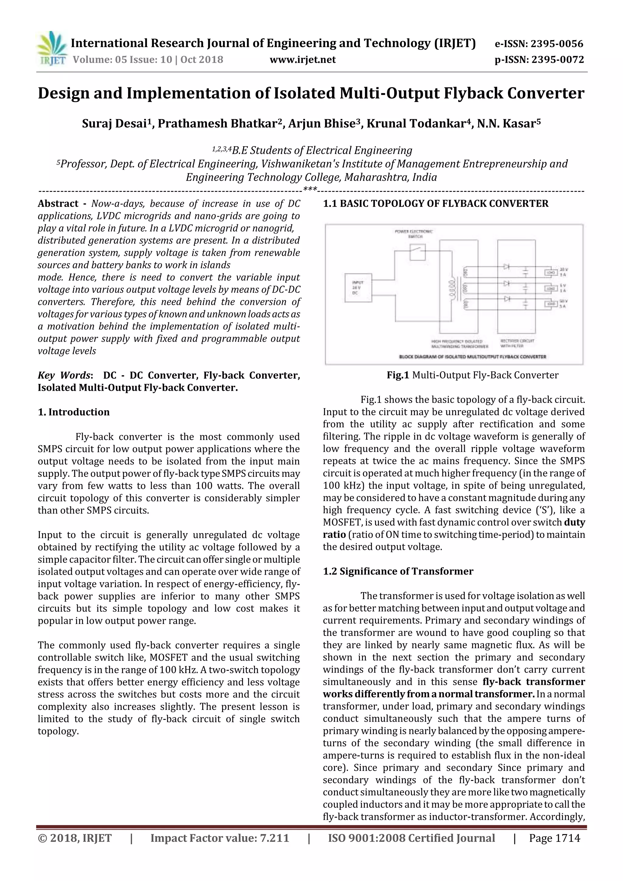
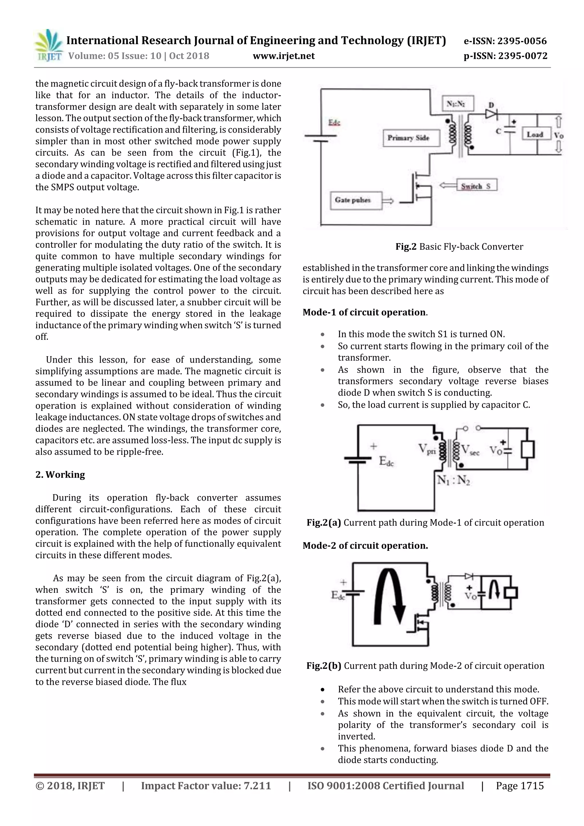
This document describes the design and implementation of an isolated multi-output flyback converter. A flyback converter uses a single switch and transformer to provide isolated output voltages from an input source. The designed converter uses a toroidal transformer with multiple secondary windings to generate multiple isolated output voltages at fixed levels. Simulation results and specifications for the transformer, switch, and outputs are provided. The flyback converter provides an efficient and low-cost solution for applications requiring multiple isolated low-power DC outputs.


![[IJET V2I5P12] Authors: Mr. Harikrishnan U, Dr. Bos Mathew Jos, Mr.Thomas P R...](https://cdn.slidesharecdn.com/ss_thumbnails/ijet-v2i5p12-161107141950-thumbnail.jpg?width=640&height=640&fit=bounds)


![[IJET- V2I2P17] Authors: Gaurav B. Patil., Paresh J. Shah](https://cdn.slidesharecdn.com/ss_thumbnails/ijet-v2i2p17-160609042055-thumbnail.jpg?width=640&height=640&fit=bounds)


