Downloaded 141 times

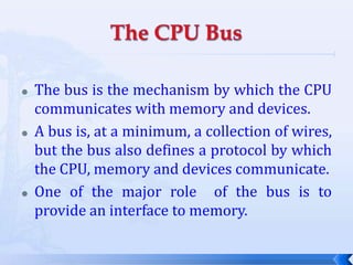
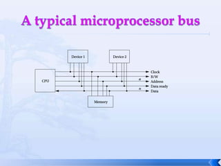
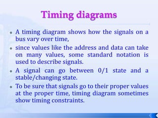
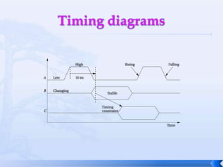
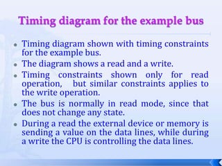
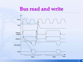
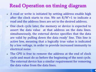
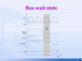
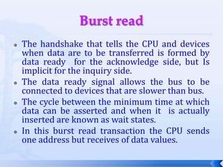
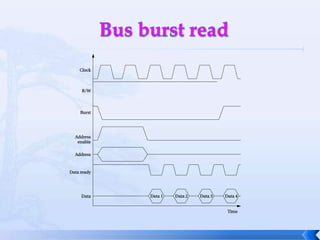
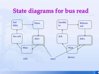
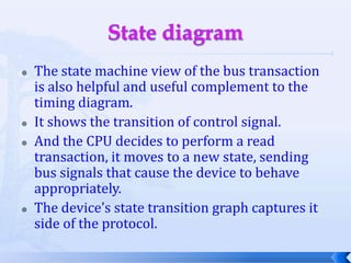
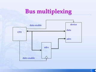
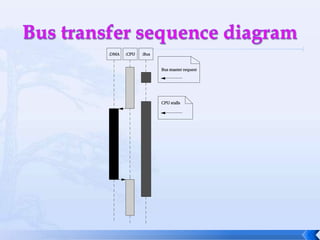
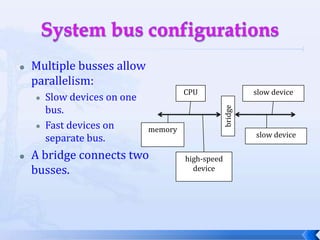
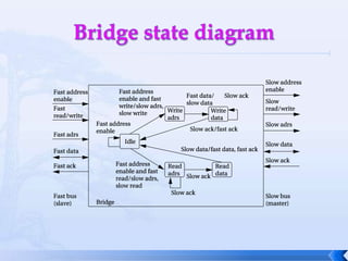
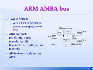

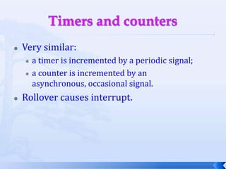
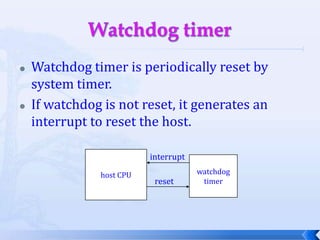
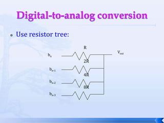
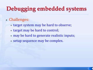
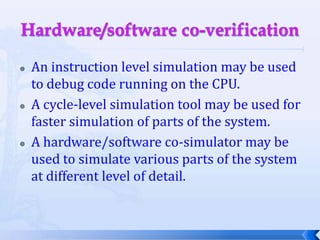
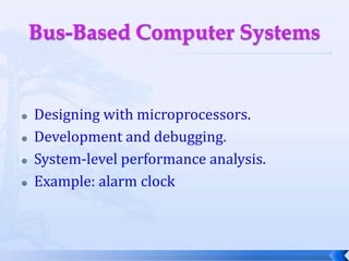
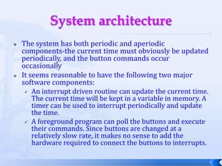
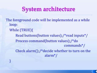
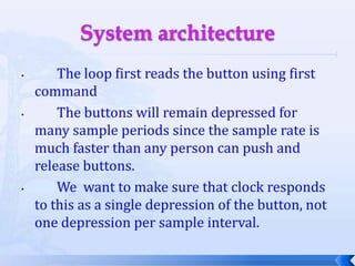

The document discusses embedded computing platforms and system architecture. It covers the CPU bus and bus protocols. It describes the four-cycle handshake protocol and timing diagrams for microprocessor buses. It discusses different types of memory devices like RAM, ROM, and flash memory. It also covers I/O devices, DMA, and system bus configurations. The software architecture and relationship with hardware architecture is explained. Debugging embedded systems using host/target design is also summarized.