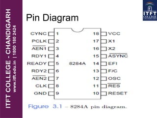
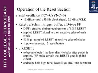
Clock Generator
8284
Clock Generator 8284
• The 8284A is an integrated circuit designed
specifically for use with the 8086/8088 micro-
processors.
• Without the clock generator, many additional
circuits are required to generate the clock (CLK) in
an 8086/8088-based system.
• The 8284 is an 18 pin integrated circuit , designed
specifically for use with 8086 microprocessor.
This circuit provides the following basic functions or
signals
Pin Diagram
Pin Description
• CSYNC: The clock synchronization pin is used
whenever the EFI input provides synchronization
in systems with multiple processors. If the
internal crystal oscillator is used, this pin must be
ignored.
• PCLK: The peripheral clock signal is one-sixth the
crystal or EFI input frequency, and has a 50-
percent duty cycle. The PCKL output provides a
clock signal; to the peripheral equipment in the
system.
• AEN1 & AEN2 : The address enable pins are
provided to qualify the bus ready signal, RDY1 &
RDY2 . These two pins are used to cause wait
state, along with RDY1 & RDY2 inputs.
• Wait state are generated by the READY pin of the
8086 microprocessor which is controlled by
these two pins.
• RDY1 & RDY2: The bus ready inputs are
provided, in conjunction with the AEN1 & AEN2
pins, to cause wait state in 8086 based system.
.
• READY: READY is an output pin that connects to
the 8086/8088 READY input.
• This signal is synchronized with the RDY1 and
RDY2 Inputs.
• CLK: Provides CLK input signal to the 8086/8088
microprocessors and other components in the
system.
• GND: Connects to ground.
• Vcc : Connects to +5.0V with a tolerance of +10
percent.
• .
.
• RESET: The RESET output connects to the
8086/8088 RESET input pin.
• RES (Reset input): Active low input. Often
connects to an RC network that provides power
-on-resetting.
• OSC (Oscillator): TTL level signal output.
Provides an EFI input to other 8284A clock
generators in some multiple processor systems.
.
• F/C(Frequency/Crystal select): It chooses the
clocking source for the 8284A.
• F/C=1(high), an external clock is provided to the
EFI input pin.
• F/C=0(low), an external crystal oscillator
connected to X1 and X2 provides the clock.
• EFI(External Frequency Input): It is used when
F/C pin is set to high.
• It Supplies the timing whenever the F/C is high.
.
ASYNC(Ready synchronization)
• The ready synchronization selection input selects
either one or two stages of synchronization for
the RDY1 and RDY2 inputs.
X1 nad X2(Crystal inputs)
• An external crystal oscillator is connected to these
inputs.
• It is used as the timing source for the clock
generator and all its functions.
Ch.9 8086/8088 Hardware Specifications 10
internal block diagram of 8284A clock generator
.
Ch.9 8086/8088 Hardware Specifications 11
Operation of Clock Section
• F/C’ = 0 : internal crystal oscillator
• crystal is attached X1, X2, oscillator generate square-
wave signal at the same frequency as crystal
• square-wave signal : fed to AND gate, inverter(OSC)
• OSC output : sometimes used as EFI to other 8284A
• AND gate : select oscillator or EFI
• F/C’=0 : oscillator output → divide-by-3 counter
• F/C’=1 : EFI → divide-by-3 counter
• output of divide-by-3 counter
• timing for ready synchronization
• signal for another divide-by-2 counter : PCLK
• CLK signal : buffered before CLK output pin
Ch.9 8086/8088 Hardware Specifications 12
Operation of the Reset Section
crystal oscillator(F/C’=CSYNC=0)
• 15MHz crystal : 5MHz clock signal, 2.5MHz PCLK
• Reset : a Schmitt trigger buffer, a D-type FF
• D FF : ensured timing requirements of 8086 RESET
• applied RESET signal to µ on negative edge of each
clock
• 8086 µ : sampled RESET at positive edge of clocks
• 1. power on reset, 2. reset button
• µ RESET :
• to become logic 1 no later than 4 clocks after power is
applied, (FF make certain that RESET goes high in4
clock)
• and to be held high for at least 50 ㎲ (RC time constant)

ITFT_Clock generator

  • 1.
  • 2.
    Clock Generator 8284 •The 8284A is an integrated circuit designed specifically for use with the 8086/8088 micro- processors. • Without the clock generator, many additional circuits are required to generate the clock (CLK) in an 8086/8088-based system. • The 8284 is an 18 pin integrated circuit , designed specifically for use with 8086 microprocessor. This circuit provides the following basic functions or signals
  • 3.
  • 4.
    Pin Description • CSYNC:The clock synchronization pin is used whenever the EFI input provides synchronization in systems with multiple processors. If the internal crystal oscillator is used, this pin must be ignored. • PCLK: The peripheral clock signal is one-sixth the crystal or EFI input frequency, and has a 50- percent duty cycle. The PCKL output provides a clock signal; to the peripheral equipment in the system.
  • 5.
    • AEN1 &AEN2 : The address enable pins are provided to qualify the bus ready signal, RDY1 & RDY2 . These two pins are used to cause wait state, along with RDY1 & RDY2 inputs. • Wait state are generated by the READY pin of the 8086 microprocessor which is controlled by these two pins. • RDY1 & RDY2: The bus ready inputs are provided, in conjunction with the AEN1 & AEN2 pins, to cause wait state in 8086 based system.
  • 6.
    . • READY: READYis an output pin that connects to the 8086/8088 READY input. • This signal is synchronized with the RDY1 and RDY2 Inputs. • CLK: Provides CLK input signal to the 8086/8088 microprocessors and other components in the system. • GND: Connects to ground. • Vcc : Connects to +5.0V with a tolerance of +10 percent. • .
  • 7.
    . • RESET: TheRESET output connects to the 8086/8088 RESET input pin. • RES (Reset input): Active low input. Often connects to an RC network that provides power -on-resetting. • OSC (Oscillator): TTL level signal output. Provides an EFI input to other 8284A clock generators in some multiple processor systems.
  • 8.
    . • F/C(Frequency/Crystal select):It chooses the clocking source for the 8284A. • F/C=1(high), an external clock is provided to the EFI input pin. • F/C=0(low), an external crystal oscillator connected to X1 and X2 provides the clock. • EFI(External Frequency Input): It is used when F/C pin is set to high. • It Supplies the timing whenever the F/C is high.
  • 9.
    . ASYNC(Ready synchronization) • Theready synchronization selection input selects either one or two stages of synchronization for the RDY1 and RDY2 inputs. X1 nad X2(Crystal inputs) • An external crystal oscillator is connected to these inputs. • It is used as the timing source for the clock generator and all its functions.
  • 10.
    Ch.9 8086/8088 HardwareSpecifications 10 internal block diagram of 8284A clock generator .
  • 11.
    Ch.9 8086/8088 HardwareSpecifications 11 Operation of Clock Section • F/C’ = 0 : internal crystal oscillator • crystal is attached X1, X2, oscillator generate square- wave signal at the same frequency as crystal • square-wave signal : fed to AND gate, inverter(OSC) • OSC output : sometimes used as EFI to other 8284A • AND gate : select oscillator or EFI • F/C’=0 : oscillator output → divide-by-3 counter • F/C’=1 : EFI → divide-by-3 counter • output of divide-by-3 counter • timing for ready synchronization • signal for another divide-by-2 counter : PCLK • CLK signal : buffered before CLK output pin
  • 12.
    Ch.9 8086/8088 HardwareSpecifications 12 Operation of the Reset Section crystal oscillator(F/C’=CSYNC=0) • 15MHz crystal : 5MHz clock signal, 2.5MHz PCLK • Reset : a Schmitt trigger buffer, a D-type FF • D FF : ensured timing requirements of 8086 RESET • applied RESET signal to µ on negative edge of each clock • 8086 µ : sampled RESET at positive edge of clocks • 1. power on reset, 2. reset button • µ RESET : • to become logic 1 no later than 4 clocks after power is applied, (FF make certain that RESET goes high in4 clock) • and to be held high for at least 50 ㎲ (RC time constant)