UNIT 2 -8086 SYSTEM BUS STRUCTURE
8086 signals – Basic configurations – System bus timing – I/O
programming – Introduction to Multiprogramming – Multiprocessor
configurations – Coprocessor, Closely coupled and loosely Coupled
configurations
CO-Illustrate the detailed hardware and software structure of
the microprocessor
3.
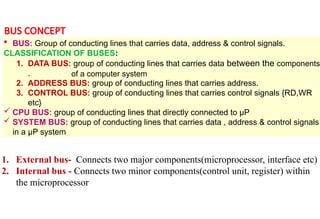
1. External bus-Connects two major components(microprocessor, interface etc)
2. Internal bus - Connects two minor components(control unit, register) within
the microprocessor
BUS CONCEPT
BUS: Group of conducting lines that carries data, address & control signals.
CLASSIFICATION OF BUSES:
1. DATA BUS: group of conducting lines that carries data between the components
.
2. ADDRESS BUS: group of conducting lines that carries address.
3. CONTROL BUS: group of conducting lines that carries control signals {RD,WR
etc}
CPU BUS: group of conducting lines that directly connected to µP
SYSTEM BUS: group of conducting lines that carries data , address & control signals
in a µP system
of a computer system
4.
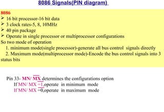
8086
16 bitprocessor-16 bit data
3 clock rates-5, 8, 10MHz
40 pin package
Operate in single processor or multiprocessor configurations
So two mode of operation
1. minimum mode(single processor)-generate all bus control signals directly
2. Maximum mode(multiprocessor mode)-Encode the bus control signals into 3
status bits
8086 Signals(PIN diagram)
Pin 33- MN/ MX determines the configurations option
If MN/ MX =1,operate in minimum mode
If MN/ MX =0,operate in maximum mode
In 8086 threegroup of signals are present
1. Signals having common functions in minimum & maximum mode
2. Signals having special functions in minimum mode
3. Signals having special functions in maximum mode
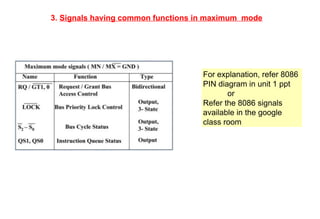
1. Signals having common functions in minimum & maximum mode
For explanation, refer 8086
PIN diagram in unit 1 ppt
or
Refer the 8086 signals
available in the google
class room
8.
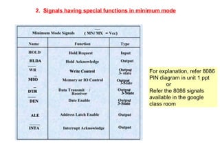
2. Signals havingspecial functions in minimum mode
For explanation, refer 8086
PIN diagram in unit 1 ppt
or
Refer the 8086 signals
available in the google
class room
9.
3. Signals havingcommon functions in maximum mode
For explanation, refer 8086
PIN diagram in unit 1 ppt
or
Refer the 8086 signals
available in the google
class room
10.
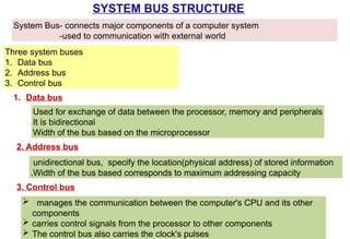
SYSTEM BUS STRUCTURE
SystemBus- connects major components of a computer system
-used to communication with external world
Three system buses
1. Data bus
2. Address bus
3. Control bus
1. Data bus
Used for exchange of data between the processor, memory and peripherals
It is bidirectional
Width of the bus based on the microprocessor
2. Address bus
unidirectional bus, specify the location(physical address) of stored information
.Width of the bus based corresponds to maximum addressing capacity
3. Control bus
manages the communication between the computer's CPU and its other
components
carries control signals from the processor to other components
The control bus also carries the clock's pulses
11.
T -cycle
One clock period is referred as a T –state
An operation takes an integer number of clock states
Processor bus cycle(machine cycle)
A processor bus cycle consists of 4 or more T states
These are referred to as T1, T2, T3, T4.
The address is transmitted by the processor during T1, and present on the
bus only for one cycle.
The negative edge of this ALE pulse is used to separate the address and the
data or status information.
The time taken to perform a bus cycle is specified in terms of term T- states.
basic operations performed by the CPU bus are called bus cycles
8086 has a combined address and data bus (multiplexed) to maximize the
utilization of processor .
The bus can be demultiplexed using a few latches and transreceivers, whenever
required.
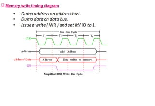
System Bus Timing
reading a byte from memory or writing a byte to a port is called machine cycle
12.
In maximummode, the status lines S0, S1 and S2 are used to indicate the type of
operation.
Status bits S3 to S7 are multiplexed with higher order address bits and the BHE
signal.
Address is valid during T1 while status bits S3 to S7 are valid during T2 through T4.
Memory Read timing diagram
Bus cycles can be classified as ● Memory read cycle● Memory write cycle● I/O read
cycle● I/O write cycle● Interrupt acknowledge cycle
BASIC CONFIGURATIONS
8086 operatein single processor or multiprocessor configurations
So two mode of operation
1. Minimum mode (single processor) configurations- generate all bus control
signals directly
2. Maximum mode(multiprocessor mode) configuration-Encode the bus control
signals into 3 status bits
Pin 33- MN/ MX determines the configurations option
If MN/ MX =1,operate in minimum mode
If MN/ MX =0,operate in maximum mode
17.
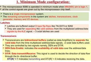
1. Minimum Modeconfiguration:
The microprocessor 8086 is operated in minimum mode when MN/(MX)’ pin is logic 1.
all the control signals are given out by the microprocessor chip itself.
There is a single microprocessor system.
The remaining components in the system are latches, transreceivers, clock
generator, memory and I/O devices. .
Latches are buffered output D-type flip-flops like 74LS373 or 8282
They are used for separating the valid address from the multiplexed address/data
signals by the ALE signal. – 3 octal latches are used
Latches
Transreceivers
Transreceivers are bidirectional buffers (called as data Amplifiers) to separate the
valid data from the time multiplexed address/data signals. -2 octal data buffers uesd.
They are controlled by two signals namely, DEN and DT/R.
DEN Data Enable: indicates the availability of valid data over the address/data
lines.
DT/R: Data transmit/Receive: This signal is used to decide the direction of data flow
through the bi- directional buffer.
DT/(R)’ = 1 Indicates transmitting and DT/(R)’ = 0 indicates receiving the data.
18.
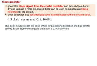
generates clocksignal from the crystal oscillator and then shapes it and
divides to make it more precise so that it can be used as an accurate timing
reference for the system.
clock generator also synchronizes some external signal with the system clock.
Clock generator
3 clock rates are used -5, 8, 10MHz
The clock input provides the basic timing for processing operation and bus control
activity. Its an asymmetric square wave with a 33% duty cycle.
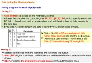
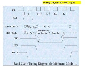
Bus timing forMinimum Mode:
timing diagram for read (input) cycle
valid address is placed on the Address/Data bus
Address latch enable the control signals M / IO* , (ALE) , DT, which specify memory or
I/O, latch the address on the address bus and set the direction of data transfer in
the data bus
BHE* and A0 signals specify the data is lower bytes , higher bytes or word.
During T1
During T2
address is removed from the local bus and is sent to the output.
read (RD*) signal is activated and causes the addressed device to enable its data bus
drivers.
DEN*. indicates the availability of valid data over the address/data lines.
Status bits S3 to S7 are multiplexed with
higher order address bits and the BHE signal.
Address is valid during T1 while status bits
S3 to S7 are valid during T2 through T4
21.
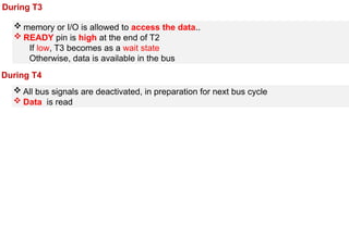
During T3
memoryor I/O is allowed to access the data..
READY pin is high at the end of T2
If low, T3 becomes as a wait state
Otherwise, data is available in the bus
During T4
All bus signals are deactivated, in preparation for next bus cycle
Data is read
timing diagram forwrite(output) cycle
write cycle begins with the assertion of ALE and the emission of the address. The
M/IO* signal is asserted to indicate a memory or I/O operation.
In T2 after sending the address in Tl, the processor sends the data to be written to the
addressed location.
The data remains on the bus until middle of T4 state.
The WR* becomes active at the beginning of T2
The BHE* and A0 signals are used to select the proper bytes of memory or I/O
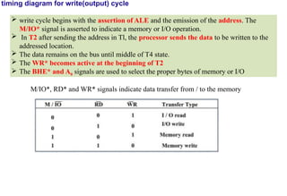
M/IO*, RD* and WR* signals indicate data transfer from / to the memory
timing diagram forHOLD cycle
HOLD, HLDA-Hold/Hold Acknowledge:
When HOLD =1, means another master is requesting the bus access.
Then processor set HLDA pin=1, in the middle of the next clock cycle after completing
the current bus (instruction) cycle(during T4).
At the same time, the processor floats the local bus and control lines.
When the processor detects the HOLD line low, it lowers the HLDA signal.
26.
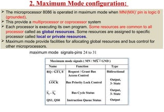
2. Maximum Modeconfiguration:
The microprocessor 8086 is operated in maximum mode when MN/(MX)’ pin is logic 0
(grounded).
This provide a multiprocessor or coprocessor system
Each processor is executing its own program. Some resources are common to all
processor called as global resources. Some resources are assigned to specific
processor called local or private resources.
Maximum mode provide facilities for allocating global resources and bus control for
other microprocessors.
maximum mode signals-pins 24 to 31
28.
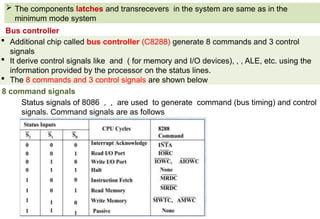
Additional chipcalled bus controller (C8288) generate 8 commands and 3 control
signals
It derive control signals like and ( for memory and I/O devices), , , ALE, etc. using the
information provided by the processor on the status lines.
The 8 commands and 3 control signals are shown below
8 command signals
Bus controller
The components latches and transrecevers in the system are same as in the
minimum mode system
Status signals of 8086 , , are used to generate command (bus timing) and control
signals. Command signals are as follows
29.
Three control signalsare , DT/ , ALE,
They have same function as minimum mode
The , and signals in Minimum mode are replaced by:
- memory read command
- memory write command
- I/O read command
- I/O write command
- Advanced memory write command
- Advanced I/O write command
pin is used to issue two interrupt acknowledge pulses to the interrupt controller or to an
interrupting device
Advanced write command signals and are used to write the data to the I/O port or
memory, but are activated one clock cycle earlier than the and signals.
30.
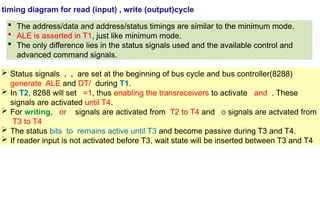
timing diagram forread (input) , write (output)cycle
The address/data and address/status timings are similar to the minimum mode.
ALE is asserted in T1, just like minimum mode.
The only difference lies in the status signals used and the available control and
advanced command signals.
Status signals , , are set at the beginning of bus cycle and bus controller(8288)
generate ALE and DT/ during T1.
In T2, 8288 will set =1, thus enabling the transreceivers to activate and . These
signals are activated until T4.
For writing, or signals are activated from T2 to T4 and o signals are actvated from
T3 to T4
The status bits to remains active until T3 and become passive during T3 and T4.
If reader input is not activated before T3, wait state will be inserted between T3 and T4
I/O programming
I/O programmingis transfer of data, commands and status signal between input/output
devices and the CPU or memory.
Modes of transfer of information
1. Programmed I/O
2. Interrupt driven I/O
3. DMA transfer
36.
.1. Programmed I/O
I/O operations means data transfer between the I/O devices and memory or I/O devices
and CPU
In programmed I/O, I/O operations are completely controlled by CPU.
Processor software checks each of the I/O
device often
CPU executes program that initiate, direct and
terminate the I/O operations, including sensing
device status, sending read , write command
and transferring data
CPU check the status of I/O system until the
operation is completed
37.
Micro processorsupport isolated I/O system.
It partition memory from I/O via software, by having instructions that specifically access
memory and others specifically access I/O
When these instructions are decoded by the microprocessor, an appropriate control
signal is generated to activate either memory or I/O operation.
If M/ IO =1, memory operation
If M/ IO =0, I/O operation
Advantages of Programmed I/O:
• simple to implement.
•requires very little hardware support.
•CPU checks status bits periodically.
Disadvantages:
•The processor has to wait for a long time for the I/O module to be ready for either
transmission or reception of data.
•The performance of the entire system is severely degraded.
39.
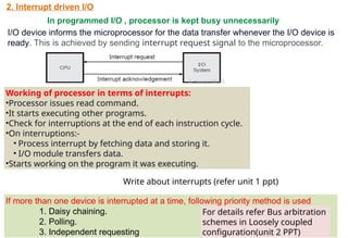
2. Interrupt drivenI/O
In programmed I/O , processor is kept busy unnecessarily
I/O device informs the microprocessor for the data transfer whenever the I/O device is
ready. This is achieved by sending interrupt request signal to the microprocessor.
Working of processor in terms of interrupts:
•Processor issues read command.
•It starts executing other programs.
•Check for interruptions at the end of each instruction cycle.
•On interruptions:-
• Process interrupt by fetching data and storing it.
• I/O module transfers data.
•Starts working on the program it was executing.
Write about interrupts (refer unit 1 ppt)
If more than one device is interrupted at a time, following priority method is used
1. Daisy chaining.
2. Polling.
3. Independent requesting
For details refer Bus arbitration
schemes in Loosely coupled
configuration(unit 2 PPT)
1.3. Direct MemoryAccess (DMA) transfer
The data transfer between any fast storage media(memory unit, magnetic disk) gets
limited with the speed of the CPU.
Therefore, DMA allow the peripherals to directly communicate with the storage using
the memory buses by removing the intervention of the CPU.
This mode of transfer of data technique is known as Direct Memory Access (DMA).
During Direct Memory Access, the CPU is idle and has no control over the memory
buses.
The DMA controller takes over the buses and directly manages data transfer between
the memory unit and I/O devices.
Used to transfer large data(block of data)
It is hardware control data transfer(DMA controller)
43.
To read ablock of data from the disk, processor sends a series of commands to
the disk controller
When disk controller is ready to transfer data, it sends request DRQ to the
DMA controller
DMA controller sends request HRQ to the processor HOLD input.
Processor responds by floating its buses and send hold acknowledgement
HLDA signal to DMA controller
DMA controller takes the control of the bus
Then DMA controller sends memory address where the data to be written and send
DMA acknowledgement DACK to disk controller, telling It to get ready to output the
data
Asserts I/O read( disk contrller to output the data) and memory write( addressed
memory accept the data From data bus) signals on the control bus.
Data is transferred without passing through the processor or DMA controller
After completion of data transfer HOLD is deassererted to give controll of all buses
back to processor
Processor is involved only at the beginning and end.,
Multiprogramming(parallel processing)
A programmingunit that perform independent task is called a process.
Multiprogramming is a technique of running several process at a time using time
sharing.
Operating system keep several process in memory simultaneously.
When a process need to wait for any I/O operation, then the CPU is switched to another
process.
Features of Multiprogramming
•Need Single CPU for implementation.
•Switching happens when current process undergoes waiting state.
•CPU idle time is reduced, High resource utilization.
•Improves system Performance by overlapping I/O operation and CPU operation.
Disadvantages of Multiprogramming
•Prior knowledge of scheduling of algorithms is required.
•large number of jobs require long waiting time.
•Memory management is because all types of tasks are stored in the main memory..
46.
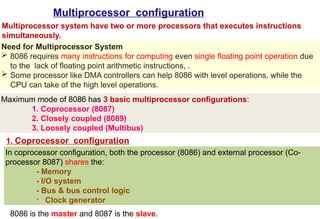
Multiprocessor configuration
Multiprocessor systemhave two or more processors that executes instructions
simultaneously.
Maximum mode of 8086 has 3 basic multiprocessor configurations:
1. Coprocessor (8087)
2. Closely coupled (8089)
3. Loosely coupled (Multibus)
In coprocessor configuration, both the processor (8086) and external processor (Co-
processor 8087) shares the:
- Memory
- I/O system
- Bus & bus control logic
- Clock generator
1. Coprocessor configuration
Need for Multiprocessor System
8086 requires many instructions for computing even single floating point operation due
to the lack of floating point arithmetic instructions, .
Some processor like DMA controllers can help 8086 with level operations, while the
CPU can take of the high level operations.
8086 is the master and 8087 is the slave.
47.
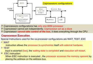
Coprocessors configurationshas only one 8086 processor
Coprocessor cannot act independently, Coprocessor act as a slave
Coprocessor cannot take control of the bus, it does everything through the CPU
Coprocessors configurations
Coprocessor Execution
WAIT
instruction allows the processor to synchronize itself with external hardware
TEST
input is asserted (low), the waiting state is completed and execution will restart.
ESC instruction:
When ESC instruction is executed , the processor accesses the memory operand by
placing the address on the address bus.
Special Instructions used for the co-processor configurations are WAIT, TEST, ESC
48.
format of ESCinstruction is ESC opcode, operand
Opcode is the instruction opcode (immediate value) recognizable to a
coprocessor
Operand is the name of a register or a memory address
Coprocessor Execution
49.
The coprocessorsends BUSY (high) to the TEST pin.
The CPU goes to the next instruction and if this is an 8086 instruction, the CPU and
coprocessor execute in parallel.
• If another coprocessor instruction occurs, the 8086 must wait until BUSY goes low ie,
TEST pin become active.
Therefore a WAIT instruction is put in front of most 8087 instructions by the Assembler.
The coprocessor also makes use of Queue Status (QS0 — QS1) of the 8086
instructions queue.
The 8086 fetches the instructions.
Coprocessor monitors the instruction sequence and captures its own instructions.
ESC is decoded by the CPU and coprocessor simultaneously.
The CPU computes the 20 bit address of memory operand.
coprocessor captures the address of the data and obtains control of the bus to load or
store as needed.
50.
2. Closely Coupledconfiguration
Closely coupled configuration has only one 8086 processor
Closely Coupled processor can take control of the bus independently
No special Instructions like WAIT, ESC is used
The communication between 8086(master/host) and 8089(independent processor) is
through Memory space
Closely coupled configuration is similar to the coprocessor configuration, i.e. both share
the same memory, I/O system, bus & bus control logic and clock generator with the host
processor. However, the coprocessor and the host processor fetches and executes their
own instructions.
closely coupled configurations
51.
Execution of closelycoupled configuration
Host sets up a task message in the memory
It wakes up independent processor by sending OUT command
Then the independent processor access the memory to read and execute the task in
parallel with the host
When the task is completed, independent processor informs the host using status bit or
interrupt request
52.
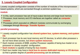
3. Loosely CoupledConfiguration
In this, each processor has set of input-output devices and large local memory
Processor, local memory and I/O interfaces are together called as computer
module.
Processes which executed on different modules communicate by exchanging
messages through Message Transfer System
Loosely coupled configuration has shared system bus, system memory, and system
I/O.
Each processor has its own local memory and I/O devices, to which other processor s
do not have direct access, but share system resources.
Each module consists of 8086, another Processor capable of being bus master or co
processor or closely coupled configuration.
Each module is capable of being the bus master.
Each bus master may have a local bus to access dedicated memory or I/O devices
so that a greater degree of parallel processing can be achieved.
parallel processing
module
Loosely coupled configuration consists of the number of modules of the microprocessor
based systems, which are connected through a common system bus.
More thanone bus master module will request access to the shared system bus at a
same time.
System bus control logic resolve the bus arbitration problem.
Simultaneous bus requests are resolved on a priority basis:
schemes for Bus arbitration (establishing priority to use system bus):
1. Daisy chaining.
2. Polling.
3. Independent requesting
1. Daisy chaining method
Daisy chaining
55.
All mastersmake use of the same line for bus request.
In response to a bus request, the bus controller sends a bus grant if the bus is free.
The bus grant signal serially propagates through each master until it encounters the
first one that is requesting access to the bus.
This master blocks the propagation of the bus grant signal, activates the busy line and
gains control of the bus.
2. Polling
All masters make use of the same line for bus request.
In response to a bus request, controller generates a sequence of master addresses.
Number of address lines required is depend on the number of masters connected in
the system.
When the requesting master recognizes the address, it activates the busy line and
begins to use the bus.
Advantage
The priority can be changed by altering the polling sequence stored in the
controller.
if one module fails entire system does not fail.
56.
3. Independent requesting
Each master has a separate pair of bus request (BRQ) and bus grant (BGR) lines and
each pair has a priority assigned to it.
The built in priority decoder within the controller selects the highest priority request
and asserts the corresponding bus grant signal.
Polling
Advantages of Multiprocessor-configuration
Better system throughput by combing more than one processor.
It is easy to add more processor for expansion as per requirement.
When a failure occurs, it is easier to detect and replace the faulty processor.
Parallel processing can be achieved
Comparsion of closely and loosely coupled
59.
Dead locks
Multiprocessorsystem suffer the problem of resource sharing
This problem occurs when two or more processors need more than one resource at
a time
None of the processor can proceed further without that resources, such situation is
referred as dead locks
Semaphore
Software technique used to solve dead locks is, mutual exclusion.
The program region where the common resources are used is called critical
program region
A binary flag called semaphore is stored in the shared memory
If semaphore = 1 , shared memory is free to access
semaphore = 0 , shared memory is busy
Setting and resetting the semaphore is performed by one processor at a time
XCHG instruction along with LOCK prefix is used to set or reset the semaphore