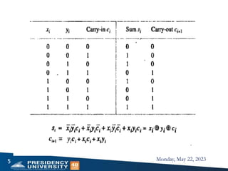
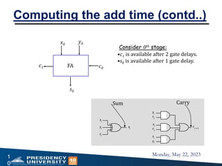
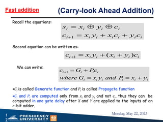
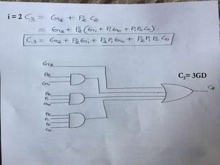
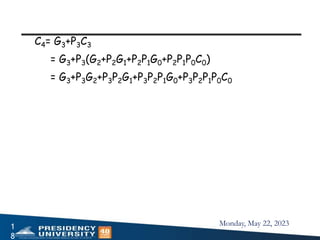
Computer Organization and Architecture
CSE 2009
Module-3: Arithmetic Unit
Monday, May 22, 2023
1
PRESIDENCY UNIVERISTY, BENGALURU, School of Engineering
Module 3a: Arithmetic Units
• Arithmetic:
• Carry lookahead Adder,
• Signed-Operand Multiplication,
• Integer Division,.
Monday, May 22, 2023
3
• A basic operation in all digital computers is the addition or
subtraction of two numbers.
• In this chapter we discuss about the logic circuits used to
implement arithmetic operations.
• The time needed to perform an addition operation affects the
processor’s performance.
• Multiply and divide operations, which require more complex
circuitry than either addition or subtraction operations, also
affect the performance.
• In this chapter we discuss about some of the techniques used
in modern computers to perform arithmetic operations at high
speed.
• Compared with arithmetic operations, logic operations are
simple to implement using combinational circuits.
Introduction
Monday, May 22, 2023
4
Consider the addition of two numbers X and Y with n-bits each.
Figure shows the logic truth table for adding equally weighted bits
Xi and Yi in two numbers X And Y.
The figure also shows the logic expressions for these functions,
along with an example of addition of 4-bit unsigned numbers 7 and
6.
The logic expression for sum (Si) and the carry out function (Ci+1)
are shown in the figure.
Addition And Subtraction Of Two Numbers
Monday, May 22, 2023
5
Monday, May 22, 2023
6
FULL ADDER:
The circuit which performs the addition of three bits is a Full
Adder.
It consists of three inputs and two outputs.
INPUTS:
Xi, yi and ci are the three inputs of full adder.
OUTPUTS:
Si and Ci+1 are the two outputs of full adder.
Block diagram of full adder is shown in the figure.
A cascaded connection of n full adder blocks can be used to add
two n-bit numbers. Since the carries must propagate or ripple
through this cascade, the configuration is called an n-bit ripple-
carry adder.
A cascaded connection of K n-bit adders can be used to add k n-bit
numbers.
Adder
Monday, May 22, 2023
7
Monday, May 22, 2023
8
Monday, May 22, 2023
9
Computing the add time
Monday, May 22, 2023
1
0
x0
y0
c0
c1
s0
FA
c
i
yi
xi
c
i
yi
x
i
xi
ci
yi
si
c
i 1
+
Sum Carry
•c1 is available after 2 gate delays.
•s0 is available after 1 gate delay.
Consider 0th stage:
Computing the add time (contd..)
Monday, May 22, 2023
1
1
x0
y0
s2
FA
x0 y0
x0
y0
s1
FA
c2
s0
FA
c1
c3
c0
x0
y0
s3
FA
c4
•s0 available after 1 gate delays, c1 available after 2 gate delays.
•s1 available after 3 gate delays, c2 available after 4 gate delays.
•s2 available after 5 gate delays, c3 available after 6 gate delays.
•s3 available after 7 gate delays, c4 available after 8 gate delays.
Cascade of 4 Full Adders, or a 4-bit adder
For an n-bit adder, sn-1 is available after 2n-1 gate delays
cn is available after 2n gate delays.
Computing the add time (contd..)
Monday, May 22, 2023
1
2
Recall the equations:
i
i
i
i
i
i
i
i
i
i
i
c
y
c
x
y
x
c
c
y
x
s






1
Second equation can be written as:
i
i
i
i
i
i c
y
x
y
x
c )
(
1 



We can write:
i
i
i
i
i
i
i
i
i
i
y
x
P
and
y
x
G
where
c
P
G
c





1
•Gi is called Generate function and Pi is called Propagate function
•Gi and Pi are computed only from xi and yi and not ci, thus they can be
computed in one gate delay after X and Y are applied to the inputs of an
n-bit adder.
Fast addition (Carry-look Ahead Addition)
Monday, May 22, 2023
1
3
• The expressions Gi and Pi are called the generate and propagate
functions for stage i.
• Each bit stage contains an
1) AND gate to form Gi,
2) OR gate to form Pi, and
3) three-input XOR gate to form Si.
• A simpler circuit can be designed to generate Gi, Si and Pi
But in this case Gi=1, so it does not matter whether Pi is 0 or 1.
Then using a cascade of two input XOR gates to realize the 3-input
XOR function. the basic cell B can be used in each bit stage as shown
in the figure.
Monday, May 22, 2023
1
4
1
5
i = 0
C1= 3GD
i = 1
C2= 3GD
i
i
i
i c
P
G
c 

1
1
6
i = 2
C3= 3GD
1
7
i = 3
C4= 3GD
Monday, May 22, 2023
1
8
C4= G3+P3C3
= G3+P3(G2+P2G1+P2P1G0+P2P1P0C0)
= G3+P3G2+P3P2G1+P3P2P1G0+P3P2P1P0C0
Monday, May 22, 2023
1
9
4-bit carry-lookahead Adder
Monday, May 22, 2023
2
0
Pi and Gi:
All Pi and Gi are available after one gate delay.
Ci+1:
All carries are available after three gate delays.
Sum:
After a further XOR gate delay, all sum bits are
available. So after four gate delays all sums are
available.
Monday, May 22, 2023
2
1
• An adder implemented in this form is called a carry-look
ahead adder.
• Delay through the adder is 3 gate delays for all carry
bits and 4 gate delays for all sum bits.
• In comparison 4-bit ripple carry adder requires 7 gate
delays for all sums and 8 gate delays for all carries.
MULTIPLICATION
MULTIPLICATION RULES
MULTIPLICATION
1. Signed-operand Multiplication using Sign-Extension Method
2. BOOTH’S Algorithm
• Considering 2’s-complement signed operands, what will happen to
(-13)(+11) if following the same method of unsigned multiplication?
Sign extension of negative multiplicand.
1
1 1
1 1 1 0 0 1 1
0
0
0
0
0
0
1
1
0
0
1
1
1
0
0
0
0
0
0
0
0
1
1
0
0
1
1
1
1
1
143
-
( )
Sign extension is
shown in blue
Signed-operand Multiplication(Sign Extension Method)
(-13) Multiplicand
X
(+11) Multiplier
(5 bits)
1 1
1
0
0
0 1
1
0
1 (5 bits)
1
0
0
1
1
1
0
1
1 0
MULTIPLICATION
BOOTH’S Algorithm
BOOTH’S Algorithm
• The booth algorithm generates the 2n-bit product and treats both
positive and negative 2’s complement n-bit operands uniformly.
• In general, in the booth scheme, -1 times the shifted multiplicand is
selected when moving from 0 to 1, and +1 times the multiplicand is
selected when moving from 1 to 0.
Example:
Recode the multiplier 101100 for Booth’s algorithm?
Multiplier: 1 0 1 1 0 0 0
Recoded Multiplier: -1 +1 0 -1 0 0
Monday, May 22, 2023
2
7
1350
+
( )
BOOTH’S Algorithm
(+45) Multiplicand
X
(+30) Multiplier
(7 bits)
0 1
1
0
1 0 1
0 1
1
1
0 (7 bits)
0
1
0
0
0
0 0
0 0
0
0
0
1 1
0
0
0 0
0 0 0 0 0 0 0
0 0
0
1
1
1 1
0
0
0
0
0
1 0 1 0 0 1 1
0 0 0 0 0 0 0
0 0 0 0 0 0 0
0 0 0 0 0 0 0
0 1 0 1 1 0 1
0 0 0 0 0 0 0
1 0 0 0 1 1 0
0 0 0 1 0 1 0
Booth Recoded Multiplier 0 1 0 0 0 -1 0 (7 bits)
Monday, May 22, 2023
2
9
Booth’s Algorithm
Monday, May 22, 2023
3
0
Monday, May 22, 2023
3
1
Integer Division
Restoring Division Algorithm
Integer Division
• The figure 6.20 shows the examples of decimal division and
binary division of the same values.
Monday, May 22, 2023
3
3
Manual Division
Circuit Arrangement for binary division
qn-1
Divisor M
Control
Sequencer
Dividend Q
Shift left
N+1 bit
adder
q0
Add/Subtract
Quotient
Setting
A
m0
0 mn-1
a0
an
an-1
Restoring Division
• Figure in the previous slide shows a logic circuit arrangement that
implements restoring division.
• An n-bit positive divisor is loaded into register M.
• An n-bit positive dividend is loaded into register Q at the start of the
operation.
• Register A is set to 0.
• After the division is complete,
n-bit Quotient  Register Q
Remainder  Register A
• The extra bit position at the end of both A and M accommodates the
sign bit during subtractions.
Monday, May 22, 2023
3
5
The following algorithm performs the restoring division:
Do the following ‘n’ times:
1. Shift A and Q left one binary position.
2. Subtract M from A, and place the answer back in A.
3. If the sign of A is 1, set Q0 to 0 and add M back to
A(that is, restore A); otherwise set Q0 to 1.
Figure 6.22 shows a 4-bit example as it would be processed by
the circuit in the figure 6.21
Monday, May 22, 2023
3
6
Restoring Division Algorithm
3
7
Restoring Division Algorithm Flowchart
3
8
Restoring Division Algorithm example 1
8 DIV 3
3
9
Restoring Division Algorithm example 1 (cont.)
Restoring Division Algorithm example 2
Monday, May 22, 2023 41
End of Module 3

COA.pptx

  • 1.
    Computer Organization andArchitecture CSE 2009 Module-3: Arithmetic Unit Monday, May 22, 2023 1 PRESIDENCY UNIVERISTY, BENGALURU, School of Engineering
  • 2.
    Module 3a: ArithmeticUnits • Arithmetic: • Carry lookahead Adder, • Signed-Operand Multiplication, • Integer Division,.
  • 3.
    Monday, May 22,2023 3 • A basic operation in all digital computers is the addition or subtraction of two numbers. • In this chapter we discuss about the logic circuits used to implement arithmetic operations. • The time needed to perform an addition operation affects the processor’s performance. • Multiply and divide operations, which require more complex circuitry than either addition or subtraction operations, also affect the performance. • In this chapter we discuss about some of the techniques used in modern computers to perform arithmetic operations at high speed. • Compared with arithmetic operations, logic operations are simple to implement using combinational circuits. Introduction
  • 4.
    Monday, May 22,2023 4 Consider the addition of two numbers X and Y with n-bits each. Figure shows the logic truth table for adding equally weighted bits Xi and Yi in two numbers X And Y. The figure also shows the logic expressions for these functions, along with an example of addition of 4-bit unsigned numbers 7 and 6. The logic expression for sum (Si) and the carry out function (Ci+1) are shown in the figure. Addition And Subtraction Of Two Numbers
  • 5.
  • 6.
    Monday, May 22,2023 6 FULL ADDER: The circuit which performs the addition of three bits is a Full Adder. It consists of three inputs and two outputs. INPUTS: Xi, yi and ci are the three inputs of full adder. OUTPUTS: Si and Ci+1 are the two outputs of full adder. Block diagram of full adder is shown in the figure. A cascaded connection of n full adder blocks can be used to add two n-bit numbers. Since the carries must propagate or ripple through this cascade, the configuration is called an n-bit ripple- carry adder. A cascaded connection of K n-bit adders can be used to add k n-bit numbers. Adder
  • 7.
  • 8.
  • 9.
    Monday, May 22,2023 9 Computing the add time
  • 10.
    Monday, May 22,2023 1 0 x0 y0 c0 c1 s0 FA c i yi xi c i yi x i xi ci yi si c i 1 + Sum Carry •c1 is available after 2 gate delays. •s0 is available after 1 gate delay. Consider 0th stage: Computing the add time (contd..)
  • 11.
    Monday, May 22,2023 1 1 x0 y0 s2 FA x0 y0 x0 y0 s1 FA c2 s0 FA c1 c3 c0 x0 y0 s3 FA c4 •s0 available after 1 gate delays, c1 available after 2 gate delays. •s1 available after 3 gate delays, c2 available after 4 gate delays. •s2 available after 5 gate delays, c3 available after 6 gate delays. •s3 available after 7 gate delays, c4 available after 8 gate delays. Cascade of 4 Full Adders, or a 4-bit adder For an n-bit adder, sn-1 is available after 2n-1 gate delays cn is available after 2n gate delays. Computing the add time (contd..)
  • 12.
    Monday, May 22,2023 1 2 Recall the equations: i i i i i i i i i i i c y c x y x c c y x s       1 Second equation can be written as: i i i i i i c y x y x c ) ( 1     We can write: i i i i i i i i i i y x P and y x G where c P G c      1 •Gi is called Generate function and Pi is called Propagate function •Gi and Pi are computed only from xi and yi and not ci, thus they can be computed in one gate delay after X and Y are applied to the inputs of an n-bit adder. Fast addition (Carry-look Ahead Addition)
  • 13.
    Monday, May 22,2023 1 3 • The expressions Gi and Pi are called the generate and propagate functions for stage i. • Each bit stage contains an 1) AND gate to form Gi, 2) OR gate to form Pi, and 3) three-input XOR gate to form Si. • A simpler circuit can be designed to generate Gi, Si and Pi But in this case Gi=1, so it does not matter whether Pi is 0 or 1. Then using a cascade of two input XOR gates to realize the 3-input XOR function. the basic cell B can be used in each bit stage as shown in the figure.
  • 14.
  • 15.
    1 5 i = 0 C1=3GD i = 1 C2= 3GD i i i i c P G c   1
  • 16.
  • 17.
  • 18.
    Monday, May 22,2023 1 8 C4= G3+P3C3 = G3+P3(G2+P2G1+P2P1G0+P2P1P0C0) = G3+P3G2+P3P2G1+P3P2P1G0+P3P2P1P0C0
  • 19.
    Monday, May 22,2023 1 9 4-bit carry-lookahead Adder
  • 20.
    Monday, May 22,2023 2 0 Pi and Gi: All Pi and Gi are available after one gate delay. Ci+1: All carries are available after three gate delays. Sum: After a further XOR gate delay, all sum bits are available. So after four gate delays all sums are available.
  • 21.
    Monday, May 22,2023 2 1 • An adder implemented in this form is called a carry-look ahead adder. • Delay through the adder is 3 gate delays for all carry bits and 4 gate delays for all sum bits. • In comparison 4-bit ripple carry adder requires 7 gate delays for all sums and 8 gate delays for all carries.
  • 22.
  • 23.
  • 24.
    MULTIPLICATION 1. Signed-operand Multiplicationusing Sign-Extension Method 2. BOOTH’S Algorithm
  • 25.
    • Considering 2’s-complementsigned operands, what will happen to (-13)(+11) if following the same method of unsigned multiplication? Sign extension of negative multiplicand. 1 1 1 1 1 1 0 0 1 1 0 0 0 0 0 0 1 1 0 0 1 1 1 0 0 0 0 0 0 0 0 1 1 0 0 1 1 1 1 1 143 - ( ) Sign extension is shown in blue Signed-operand Multiplication(Sign Extension Method) (-13) Multiplicand X (+11) Multiplier (5 bits) 1 1 1 0 0 0 1 1 0 1 (5 bits) 1 0 0 1 1 1 0 1 1 0
  • 26.
  • 27.
    BOOTH’S Algorithm • Thebooth algorithm generates the 2n-bit product and treats both positive and negative 2’s complement n-bit operands uniformly. • In general, in the booth scheme, -1 times the shifted multiplicand is selected when moving from 0 to 1, and +1 times the multiplicand is selected when moving from 1 to 0. Example: Recode the multiplier 101100 for Booth’s algorithm? Multiplier: 1 0 1 1 0 0 0 Recoded Multiplier: -1 +1 0 -1 0 0 Monday, May 22, 2023 2 7
  • 28.
    1350 + ( ) BOOTH’S Algorithm (+45)Multiplicand X (+30) Multiplier (7 bits) 0 1 1 0 1 0 1 0 1 1 1 0 (7 bits) 0 1 0 0 0 0 0 0 0 0 0 0 1 1 0 0 0 0 0 0 0 0 0 0 0 0 0 0 1 1 1 1 0 0 0 0 0 1 0 1 0 0 1 1 0 0 0 0 0 0 0 0 0 0 0 0 0 0 0 0 0 0 0 0 0 0 1 0 1 1 0 1 0 0 0 0 0 0 0 1 0 0 0 1 1 0 0 0 0 1 0 1 0 Booth Recoded Multiplier 0 1 0 0 0 -1 0 (7 bits)
  • 29.
    Monday, May 22,2023 2 9 Booth’s Algorithm
  • 30.
  • 31.
  • 32.
  • 33.
    Integer Division • Thefigure 6.20 shows the examples of decimal division and binary division of the same values. Monday, May 22, 2023 3 3 Manual Division
  • 34.
    Circuit Arrangement forbinary division qn-1 Divisor M Control Sequencer Dividend Q Shift left N+1 bit adder q0 Add/Subtract Quotient Setting A m0 0 mn-1 a0 an an-1
  • 35.
    Restoring Division • Figurein the previous slide shows a logic circuit arrangement that implements restoring division. • An n-bit positive divisor is loaded into register M. • An n-bit positive dividend is loaded into register Q at the start of the operation. • Register A is set to 0. • After the division is complete, n-bit Quotient  Register Q Remainder  Register A • The extra bit position at the end of both A and M accommodates the sign bit during subtractions. Monday, May 22, 2023 3 5
  • 36.
    The following algorithmperforms the restoring division: Do the following ‘n’ times: 1. Shift A and Q left one binary position. 2. Subtract M from A, and place the answer back in A. 3. If the sign of A is 1, set Q0 to 0 and add M back to A(that is, restore A); otherwise set Q0 to 1. Figure 6.22 shows a 4-bit example as it would be processed by the circuit in the figure 6.21 Monday, May 22, 2023 3 6 Restoring Division Algorithm
  • 37.
  • 38.
  • 39.
  • 40.
  • 41.
    Monday, May 22,2023 41 End of Module 3