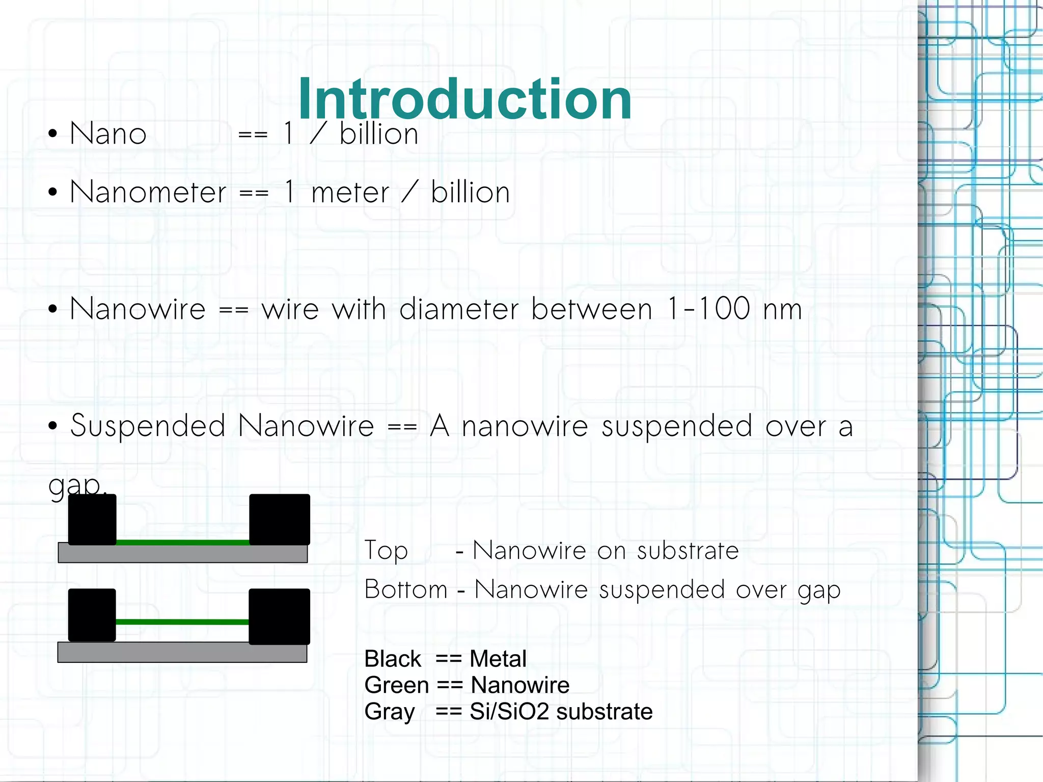
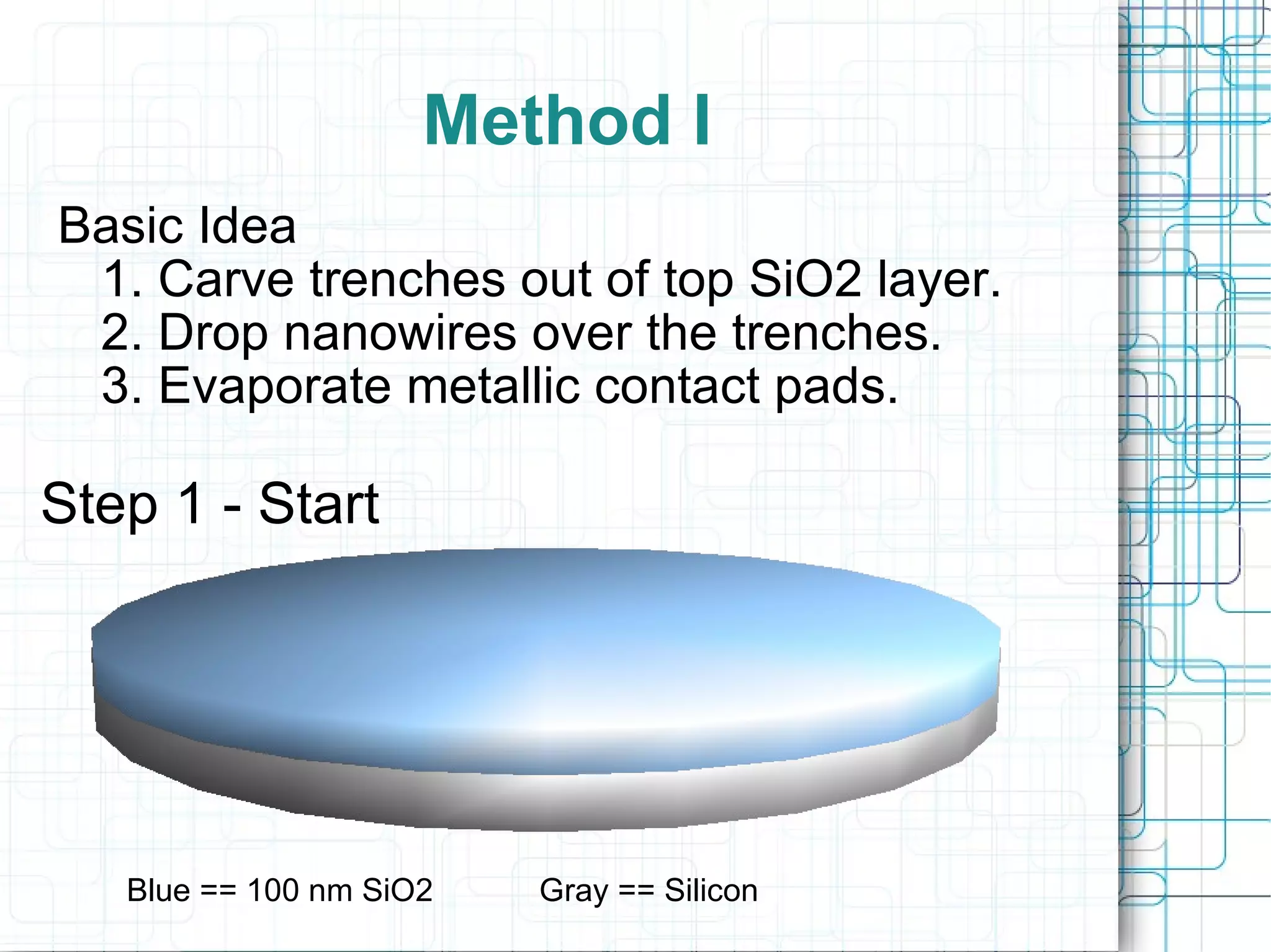
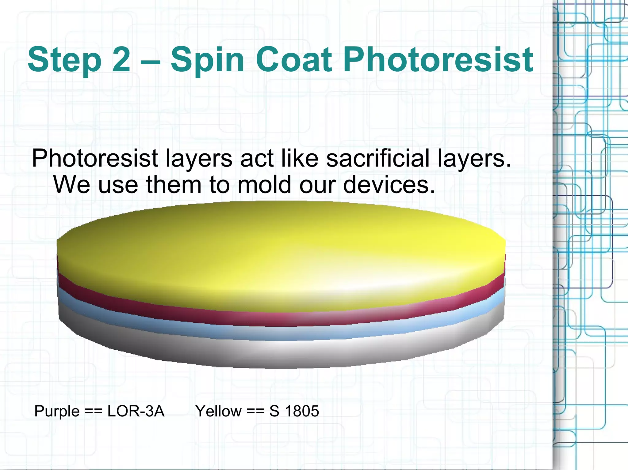
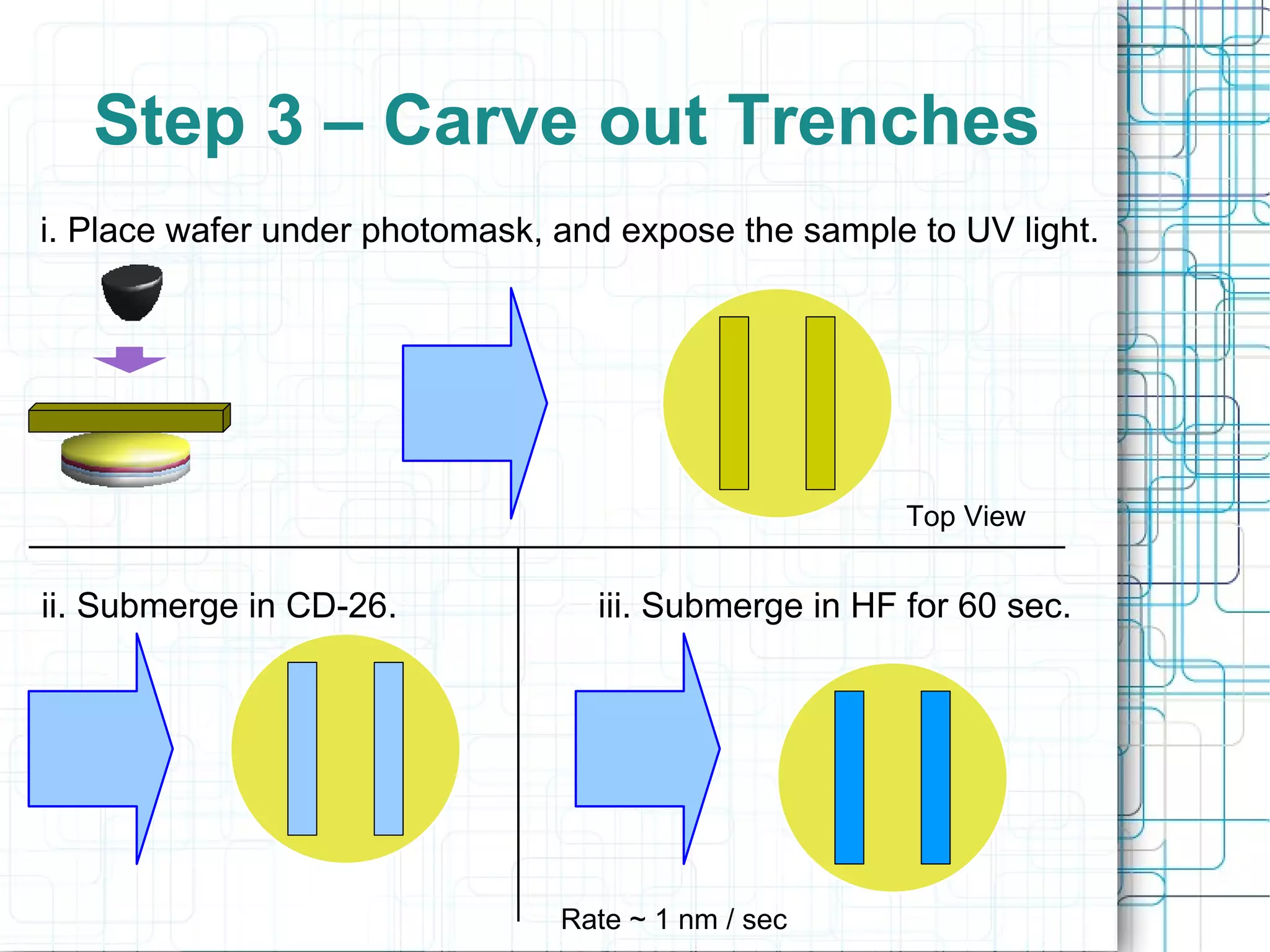
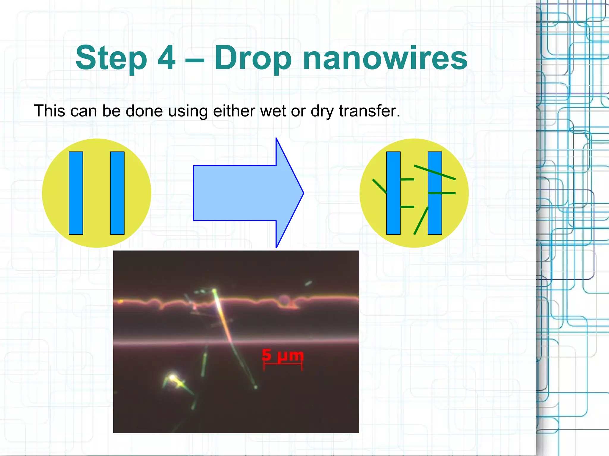
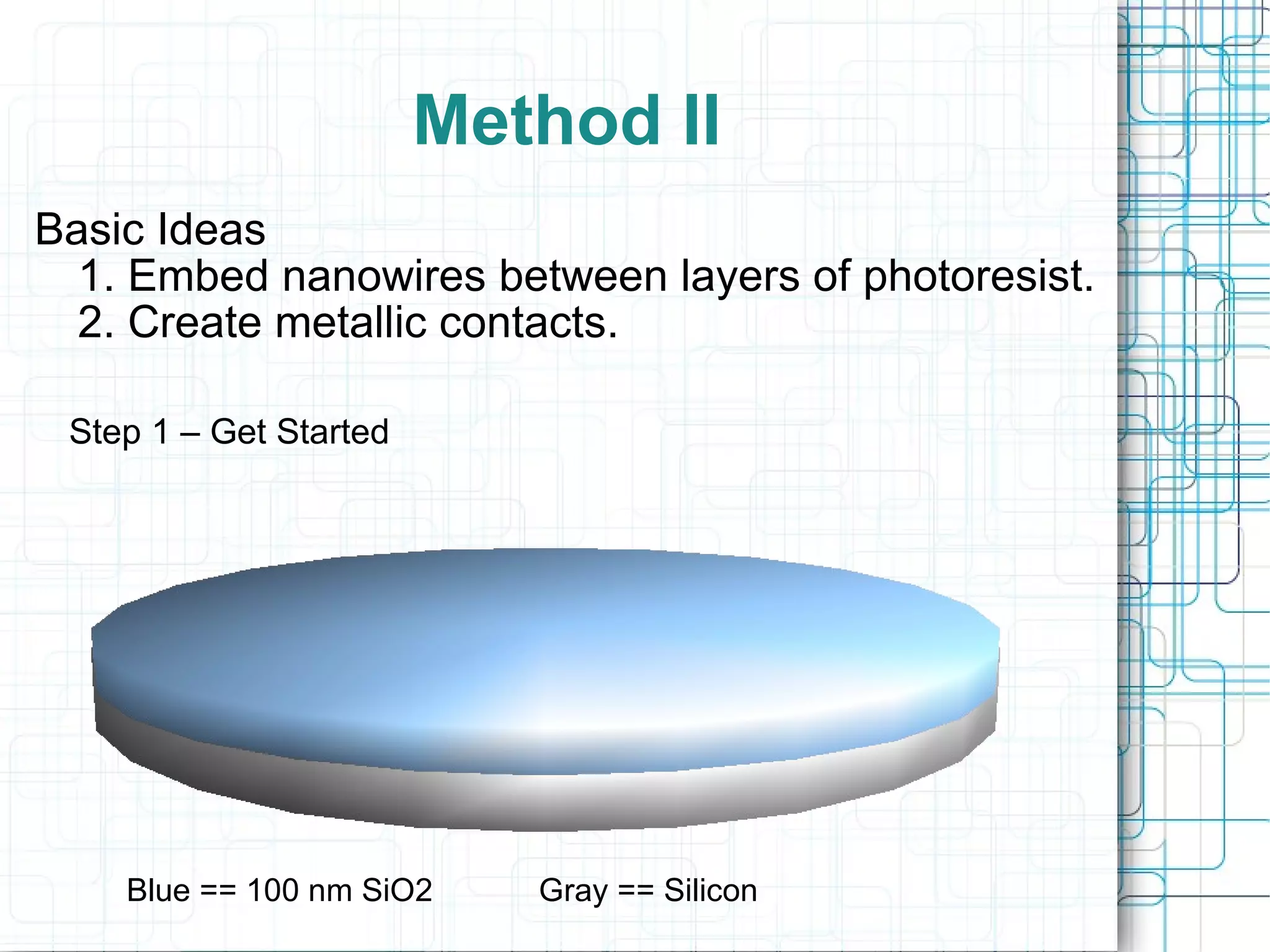
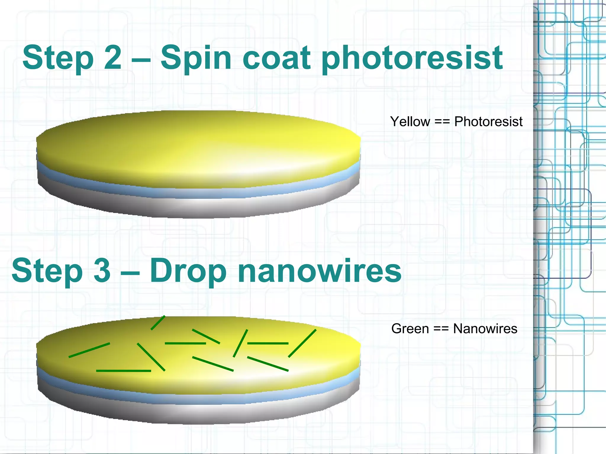
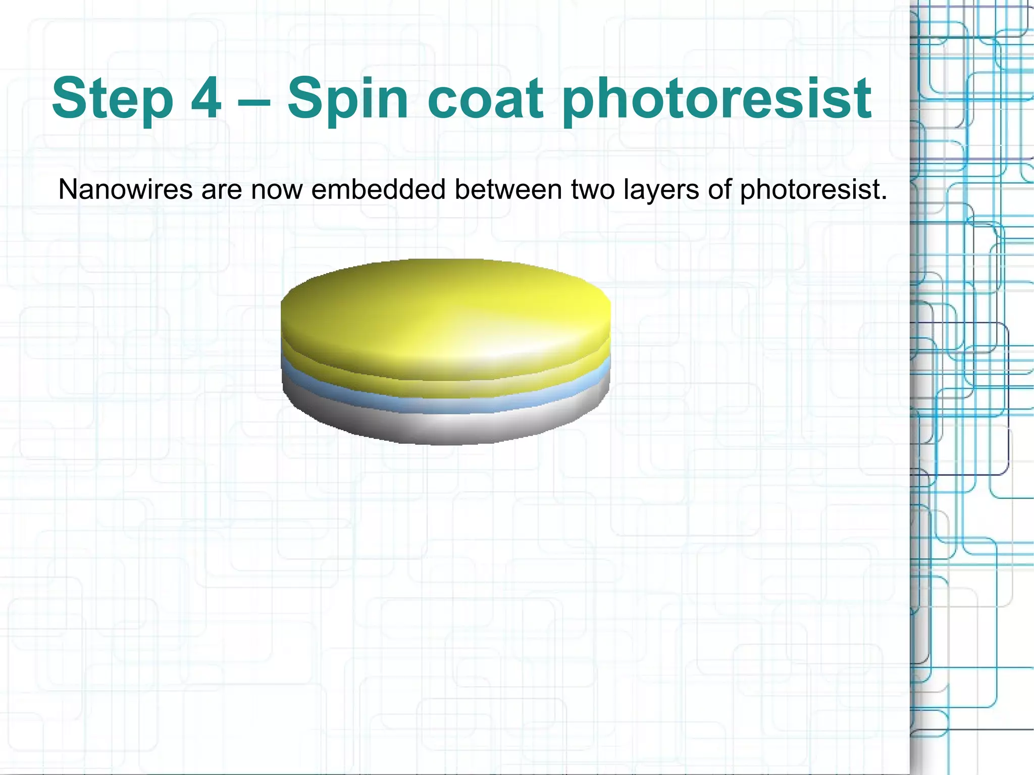
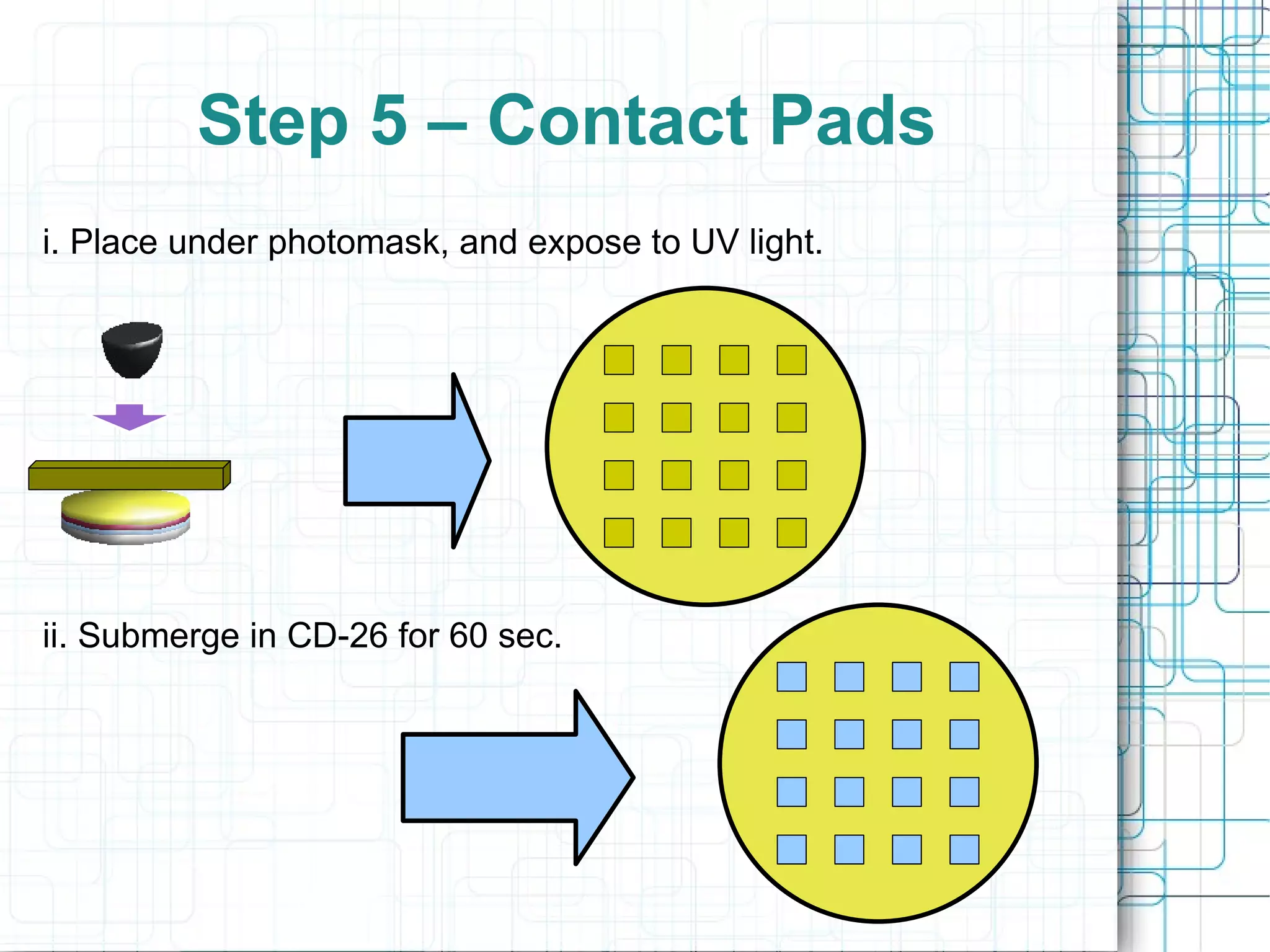
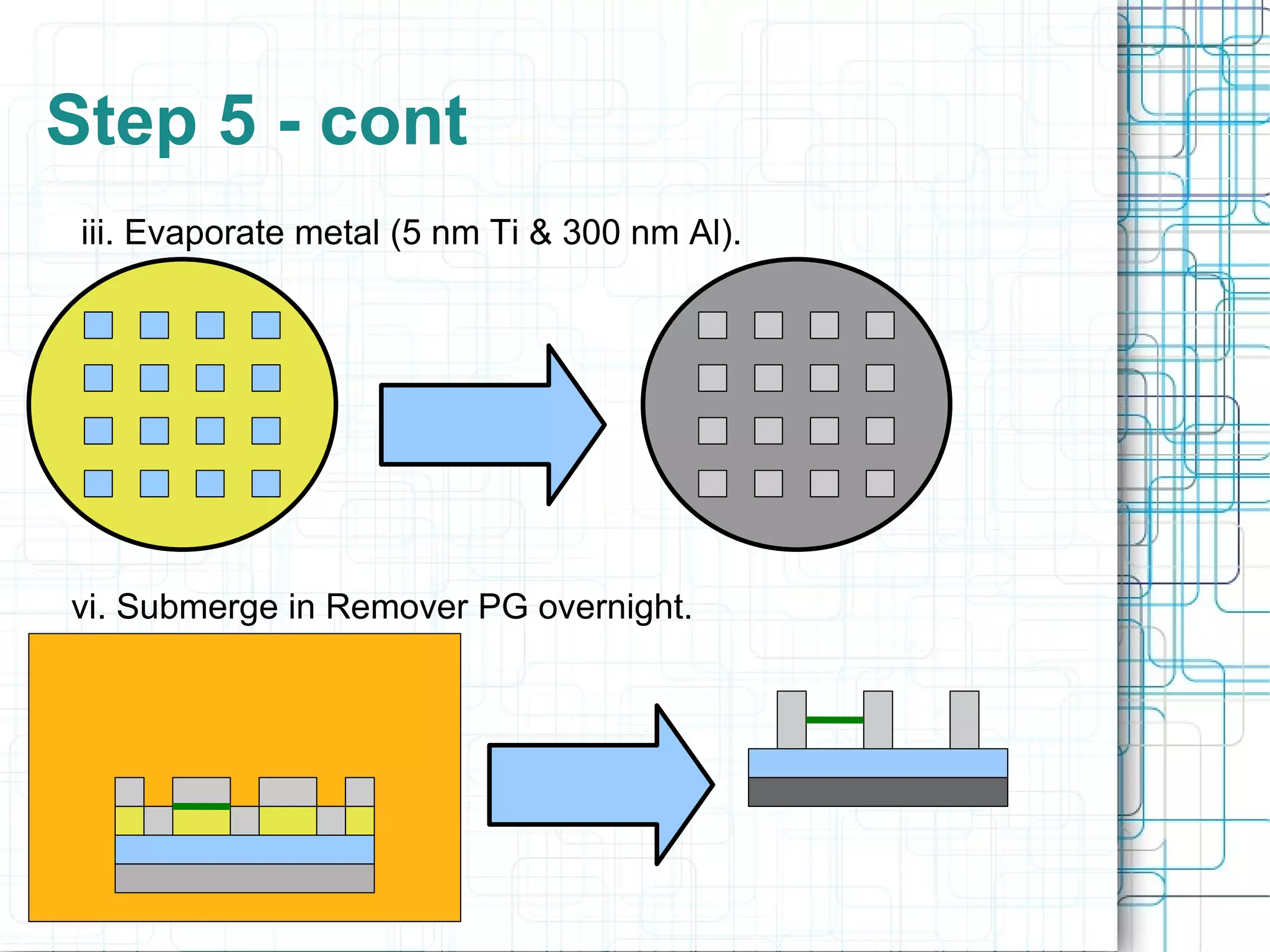
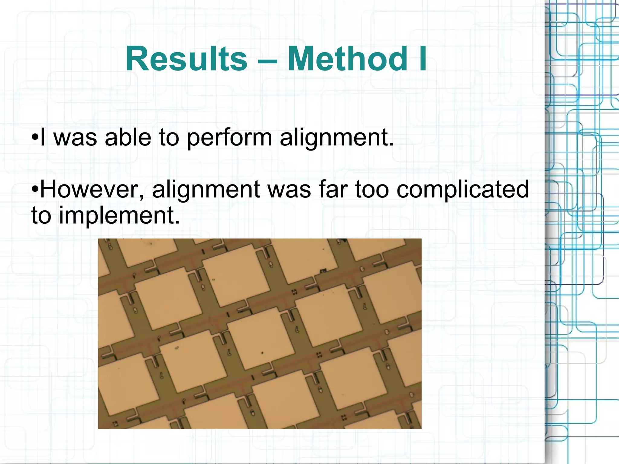
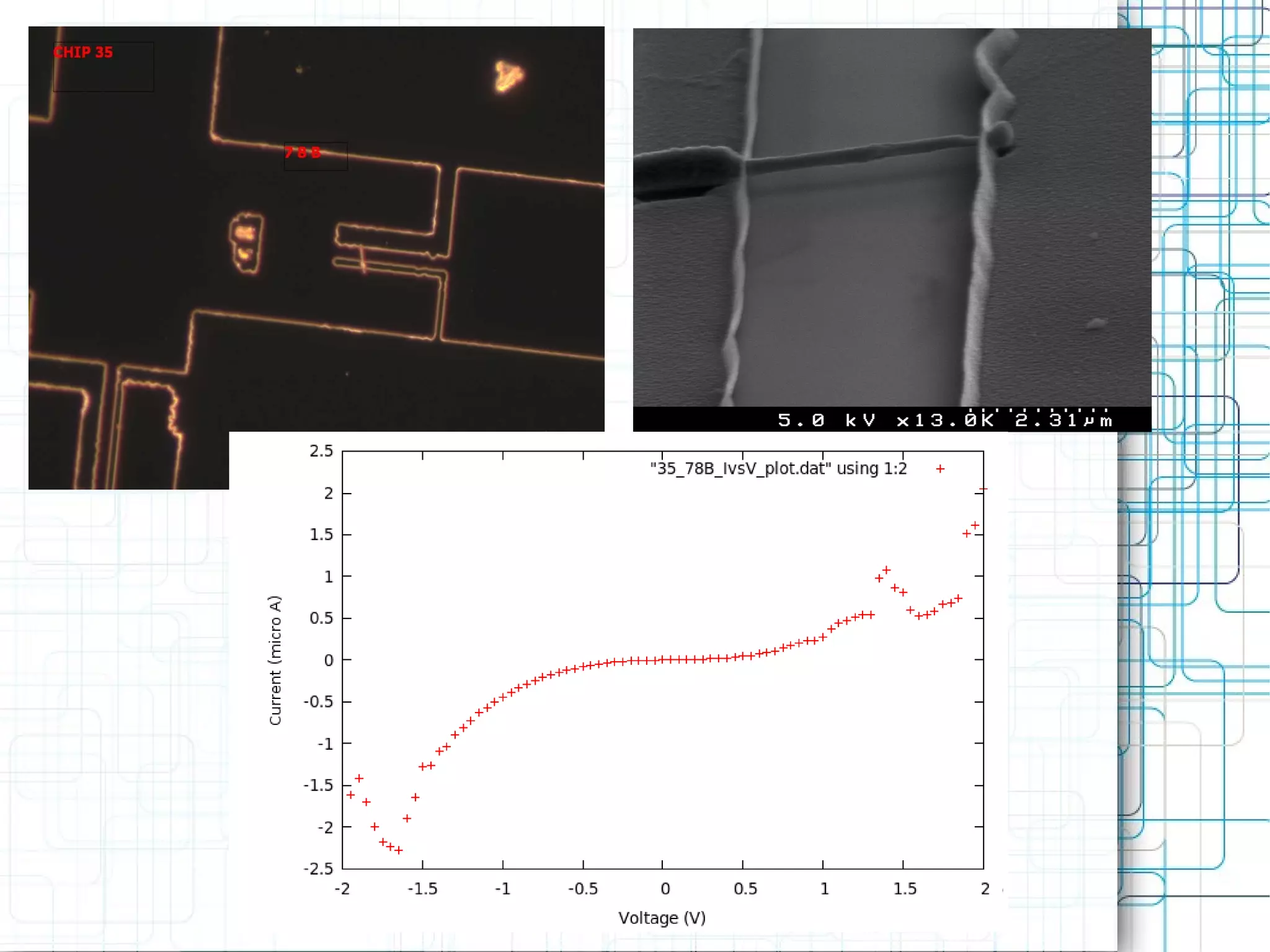
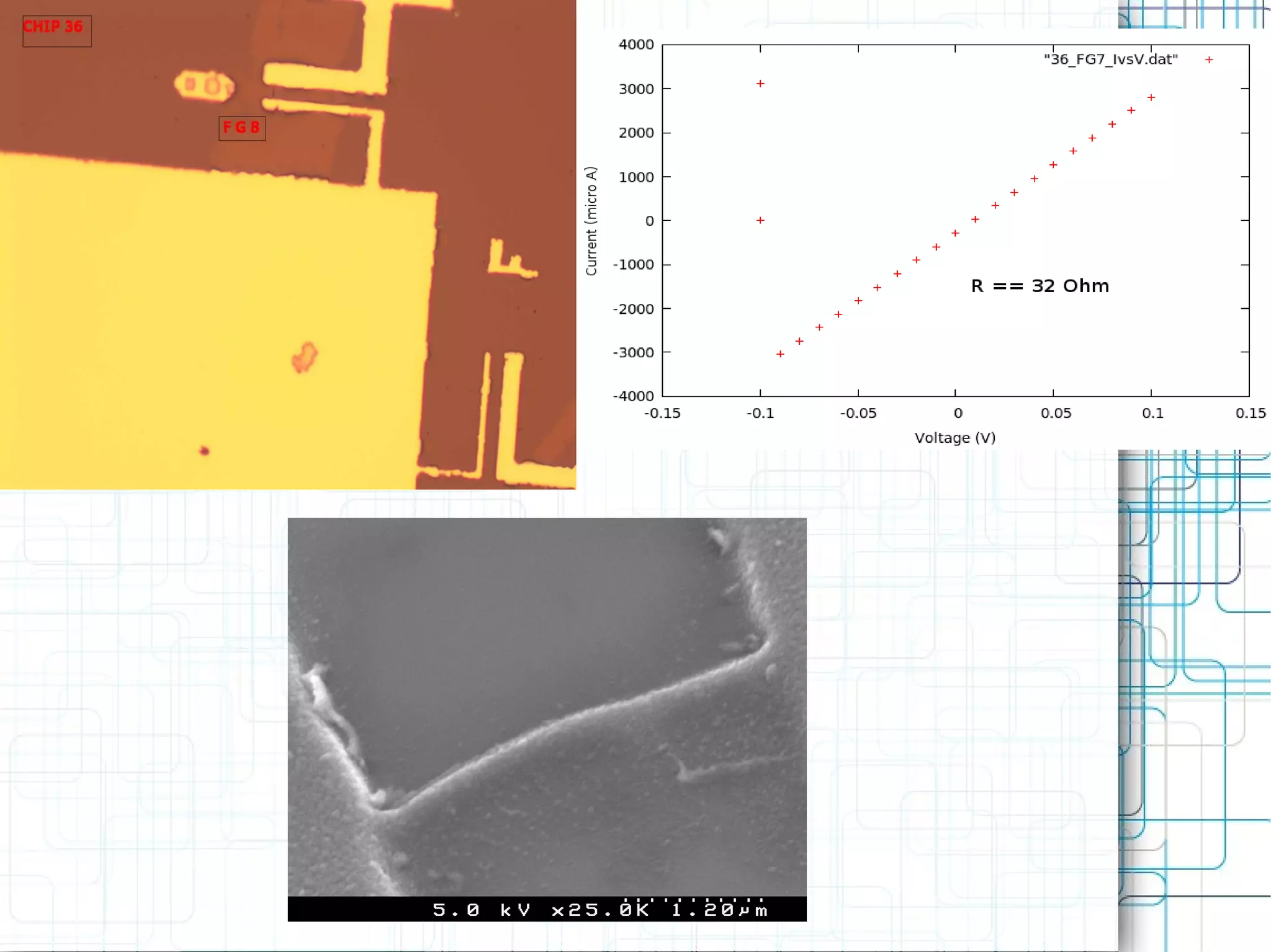
4. Goals 1. Fabricate suspended nanowire devices - Simple but not easy. 2. Test the devices and look at the I-V curves. - Should be different because the substrate (read heat sink) is not in contact with the wire.
5. Method I Basic Idea 1. Carve trenches out of top SiO2 layer. 2. Drop nanowires over the trenches. 3. Evaporate metallic contact pads. Step 1 - Start Blue == 100 nm SiO2 Gray == Silicon
6. Step 2 – Spin Coat Photoresist Photoresist layers act like sacrificial layers. We use them to mold our devices. Purple == LOR-3A Yellow == S 1805
7. Step 3 – Carve out Trenches i. Place wafer under photomask, and expose the sample to UV light. ii. Submerge in CD-26. I iii. Submerge in HF for 60 sec. Top View Rate ~ 1 nm / sec
8. Step 4 – Drop nanowires This can be done using either wet or dry transfer.
9. Step 5 – Contact Pads i. Expose 2 nd pattern to UV light. ii. Submerge in CD-26 for 60 sec.
10. Step 5 - cont. I iii. Evaporate metal (5 nm Ti & then 50 nm Al). Different shades of gray represent different elevations of metal. iv. Let the wafer sit in Remover PG overnight.
11. Method II Basic Ideas 1. Embed nanowires between layers of photoresist. 2. Create metallic contacts. Step 1 – Get Started Blue == 100 nm SiO2 Gray == Silicon
12. Step 2 – Spin coat photoresist Yellow == Photoresist Step 3 – Drop nanowires Green == Nanowires
13. Step 4 – Spin coat photoresist Nanowires are now embedded between two layers of photoresist.
14. Step 5 – Contact Pads i. Place under photomask, and expose to UV light. ii. Submerge in CD-26 for 60 sec.
15. Step 5 - cont I iii. Evaporate metal (5 nm Ti & 300 nm Al). vi. Submerge in Remover PG overnight.