
Downloaded 25 times
![Background
•
•
•
•
1920s: Cu2O rectifier
1930s: Cu2O photosensitive device
1970s: Research on Cu2O photovoltaic cells
Reported efficiency 2%. At present: 20% [1,2]
• 1980s: Three main issues of Cu2O solar cells:
1. A sound method of preparation of Cu2O
2. Increasing the photoconductivity of Cu2O
3. Making a good P-N junction [3]
3
SIMON FRASER UNIVERSITY
CANADA](https://image.slidesharecdn.com/347cu2osolarcell9-131211043036-phpapp01/85/347-cu2-o-solar-cell-9-3-320.jpg)
![Introduction
• Solar cells research - popular topic now
worldwide need for clean and renewable energy.
• Cu2O Benefits (p-type):
Availability & low cost to develop
Efficiency 20%
Band gap 2 eV[4]
• ZnO (n-type): easy to manufacture and low cost.[4]
The combination of Cu2O and ZnO
inexpensive photoconductive device.
4
SIMON FRASER UNIVERSITY
CANADA](https://image.slidesharecdn.com/347cu2osolarcell9-131211043036-phpapp01/85/347-cu2-o-solar-cell-9-4-320.jpg)
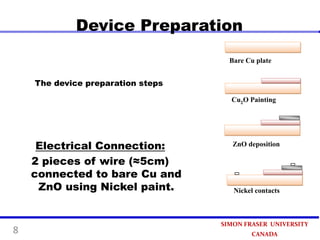
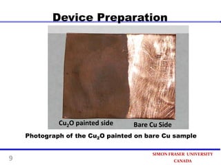
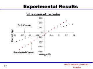
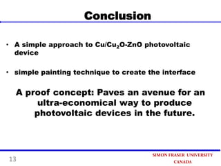

This document summarizes research on developing a low-cost photovoltaic device using copper oxide (Cu2O) and zinc oxide (ZnO). The device is prepared through three steps: 1) painting a copper sheet with a Cu2O colloidal suspension, 2) depositing ZnO using electrochemical deposition, and 3) connecting electrodes. Experimental results found a 40% increase in current when the device was illuminated, demonstrating its photovoltaic effect. The simple preparation process paves the way for an ultra-economical approach to produce photovoltaic devices in the future.


