The document summarizes research into synthesizing and characterizing zinc tin nitride (ZnSnN2). Key points:
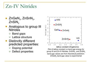
1) ZnSnN2 is analogous to indium nitride and could have a band gap of 1 eV, but has not been successfully synthesized yet.
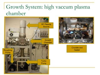
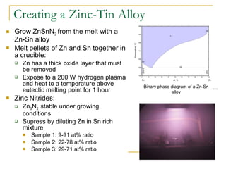
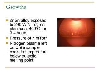
2) The researcher grew zinc-tin alloys with varying compositions and exposed them to nitrogen plasma in an attempt to form ZnSnN2.
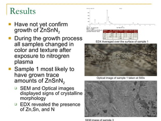
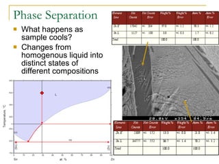
3) While ZnSnN2 was not conclusively formed, one sample showed possible trace amounts and signs of crystallinity. More analysis is still needed to confirm the results.