IOSR Journal of Electrical and Electronics Engineering (IOSR-JEEE)
e-ISSN: 2278-1676,p-ISSN: 2320-3331, Volume 6, Issue 3 (May. - Jun. 2013), PP 61-68
www.iosrjournals.org
www.iosrjournals.org 61 | Page
Secondary Distribution for Grid Interconnected Nine-level
Inverter using PV system
K. Hanumantha Rao1
, Nakeertha Suresh2
, Prof. D. Shobha Rani3
1, 2, 3
(Department of EEE, Vardhaman College of Engineering (Autonomous), JNTU Hyderabad, India)
Abstract : This paper proposes a Secondary distribution (single phase) nine -level inverter for grid-
connected photovoltaic systems, with a novel pulse width modulated (PWM) control scheme. F o u r
reference signals that are identical to each other with an offset that is equivalent to the amplitude
of the triangular carrier signal were used to generate the PWM signals. The inverter is capable of
producing nine levels of output-voltage levels (Vdc , 3Vdc /4, Vdc /2,Vdc/4, 0, −Vdc , −3Vdc
/4, −Vdc /2, Vdc/4) from the dc supply voltage. A digital proportional–integral current-control
algorithm was implemented in a TMS320F2812 DSP to keep the current injected into the grid sinusoidal. The
proposed system was verified through simulation and implemented in a prototype.
Keywords - Grid connected, modulation index, multilevel inverter, photovoltaic (PV) system, pulse width
modulated (PWM), total harmonic distortion (THD).
I. INTRODUCTION
The ever-increasing energy consumption, fossil fuels’ soaring costs and exhaustible nature, and
worsening global environment have created a booming interest in renewable energy generation systems, one of
which is photovoltaic. Such a system generates electricity by converting the Sun’s energy directly into
electricity. Photovoltaic-generated energy can be delivered to power system networks through grid-connected
inverters. A single-phase grid-connected inverter is usually used for residential or low-power applications of
power ranges that are less than 10 kW. Types of single-phase grid-connected inverters have been investigated. A
common topology of this inverter is full-bridge three-level. The three-level inverter can satisfy specifications
through its very high switching, but it could also unfortunately increase switching losses, acoustic noise, and
level of interference to other equipment. Improving its output waveform reduces its harmonic content and,
hence, also the size of the filter used and the level of electromagnetic interference (EMI) generated by the
inverter’s switching operation. Multilevel inverters are promising; they have nearly sinusoidal output-voltage
waveforms, output current with better harmonic profile, less stressing of electronic components owing to
decreased voltages, switching losses that are lower than those of conventional two-level inverters, a smaller
filter size, and lower EMI, all of which make them cheaper, lighter, and more compact. Various topologies for
multilevel inverters have been proposed over the years. Common ones are diode-clamped, flying capacitor or
multi cell, cascaded H-bridge, and modified H-bridge multilevel. This paper recounts the development of a
novel modified H-bridge single-phase multilevel inverter that has two diode embedded bidirectional switches
and a novel pulse width modulated (PWM) technique. The topology was applied to a grid-connected
photovoltaic system with considerations for a maximum-power-point tracker (MPPT) and a current-control
algorithm.
II. PROPOSED MULTILEVEL INVERTER
The proposed single-phase nine-level inverter was developed from the seven-level inverter in. It
comprises a single-phase conventional H-bridge inverter, two bidirectional switches, and a capacitor voltage
divider formed by C1, C2, C3, and C4 as shown in Fig. 1. The modified H-bridge topology is significantly
advantageous over other topologies, i.e., less power switch, power diodes, and less capacitors for inverters of
the same number of levels. Photovoltaic (PV) arrays were connected to the inverter via a dc–dc boost converter.
The power generated by the inverter is to be delivered to the power network, so the utility grid, rather than a
load, was used. The dc–dc boost converter was required. The because the PV arrays had a voltage that was lower
than the grid voltage. High dc bus voltages are necessary to ensure that power flows from the PV arrays to the
grid. A filtering inductance Lf was used to filter the current injected into the grid. Proper switching of the
inverter can produce seven output-voltage levels (Vdc, 3Vdc /4, Vdc /2, Vdc/4, 0, −Vdc, −3Vdc /4,
−Vdc/2, Vdc/4) from the dc supply voltage.
Secondary Distribution for Grid Interconnected Nine-level Inverter using PV system
www.iosrjournals.org 62 | Page
Fig. 1. Proposed single phase nine-level grid-connected inverter for photovoltaic systems.
Fig. 2. Nine-level inverter for switching operation.
The single-phase nine-level inverter was developed from the seven-level inverter as shown in Fig.1. It comprises
a single-phase conventional H-bridge inverter, three bidirectional switches, and a capacitor voltage divider
formed by C1, C2,C3 and C4, , as shown in Fig. 1. The modified H-bridge topology is significantly
advantageous over other topologies, i.e., less power switch, power diodes, and less capacitor for inverters
of the same number of levels. Photovoltaic (PV) arrays were connected to the inverter via a dc–dc boost
converter. The power generated by the inverter is to be delivered to induction Motor. The dc–dc boost converter
was required because the PV arrays had a voltage that was lower than the single-phase voltage. High dc bus
voltages are necessary to ensure that power flows from the PV arrays to the single-phase induction motor. The
LC-filter is modeled to obtain pure sine-wave and is given to drive a single-phase induction motor.. Proper
switching of the inverter can produce nine- output-voltage-levels ( Vdc, 3 V d c /4, V d c /2, V d c /4, 0 ,-Vdc/4,
-Vdc/2, -3Vdc/4, - Vdc) from the dc supply voltage. The proposed inverter’s operation can be divided into nine
switching states. The required nine levels of output voltage were generated as follows.
Maximum positive output (Vdc): S1 is ON; connecting the load positive terminal to Vdc, and S4 is
ON, connecting the load negative terminal to ground. All other controlled switches are OFF; the voltage applied
to the load terminals is Vdc.
Three-fourth positive output (3Vdc/4): The bidirectional switch S5 is ON, connecting the load
positive terminal, and S4 is ON, connecting the load negative terminal to ground. All other controlled switches
are OFF; the voltage applied to the load terminals is 3Vdc/4.
Half of the positive output (Vdc/2): The bidirectional switch S6 is ON, connecting the load positive
terminal, and S4 is ON, connecting the load negative terminal to ground. All other controlled switches are OFF;
the voltage applied to the load terminals is Vdc/2.
One-fourth of the positive output (Vdc/4): The bidirectional switch S7 is ON, connecting the load
positive terminal, and S4 is ON, connecting the load negative terminal to ground. All other controlled switches
are OFF; the voltage applied to the load terminals is Vdc/4.
Zero output: This level can be produced by two switching combinations; switches S3 and S4 are ON,
or S1 andS2 are ON, and all other controlled switches are OFF; terminal ab is a short circuit, and the voltage
applied to the load terminals is zero.
Secondary Distribution for Grid Interconnected Nine-level Inverter using PV system
www.iosrjournals.org 63 | Page
One-fourth negative output (−Vdc/4): The bidirectional switch S5 is ON, connecting the load positive
terminal, and S2 is ON, connecting the load negative terminal to Vdc. All other controlled switches are OFF;
the voltage applied to the load terminals is −Vdc/4.
Half of the negative output (−Vdc/2): The bidirectional switch S6 is ON, connecting the load
positive terminal, and S2 is ON, connecting the load negative terminal to ground. All other controlled switches
are OFF; the voltage applied to the load terminals is −Vdc/2
Three-fourth negative output (−3Vdc/4): The bidirectional switch S7 is ON, connecting the load
positive terminal, and S2 is ON, connecting the load negative terminal to ground. All other controlled switches
are OFF; the voltage applied to the load terminals is −3Vdc/4.
Maximum negative output (−Vdc): S2 is ON; connecting the load negative terminal to Vdc, and S3 is
ON, connecting the load positive terminal to ground. All other controlled switches are OFF; the voltage
applied to the load terminals is −Vdc.
Table I shows the switching combinations that generated the nine output-voltage levels (Vdc, 3Vdc/4, Vdc/2,
Vdc/4, 0,-Vdc/4, -Vdc/2, -3Vdc/4, - Vdc)
TABLE 1
Out Put Voltage According To The Switches On Off
Vo S1 S2 S3 S4 S5 S6 S7
Vdc On Off Off On Off Off Off
3Vdc/4 Off Off Off On On Off Off
Vdc/2 Off Off Off On Off On Off
Vdc/4 Off Off Off On Off Off On
0 Off Off On On Off Off Off
-Vdc/4 Off On Off Off On Off Off
-Vdc/2 Off On Off Off Off On Off
-3Vdc/4 Off On Off Off Off Off On
-Vdc Off On On Off Off Off Off
III. PWM TECHNIQUE
A novel PWM modulation technique was introduced to generate the PWM switching signals. Four
reference signals (Vref1, Vref2, Vref3, and Vref4) were compared with a carrier signal (Vcarrier). The
reference signals had the same frequency and amplitude and were in phase with an offset value that was
equivalent to the amplitude of the carrier signal. The reference signals were each compared with the carrier
signal. If Vref1 had exceeded the peak amplitude of Vcarrier, Vref2 was com- pared with Vcarrier until it
had exceeded the peak amplitudeof Vcarrier.Then, onward, Vref3 would take charge and would be compared
with Vcarrier until it had exceeded the peak amplitude of Vcarrier. Then Vref4 would take the charge to
reached zero. Once Vref4 had reached zero, Vref3 would be compared until it reached zero. Then, onward,
Vref2 would take charge to reached zero; Vref1 would be compared with Vcarrier. The resulting switching
pattern. Switches S1, S3, S5, S 6 , a n d S7 would be switching at the rate of the carrier signal frequency,
whereas S2 and S4 would operate at a frequency that was equivalent to the fundamental frequency.Fig.2 shown
signalgeneration.
Secondary Distribution for Grid Interconnected Nine-level Inverter using PV system
www.iosrjournals.org 64 | Page
Fig.2. PWM Switching signal generator.
IV. CLOSED LOOP CONTROL SYSTEM
The control system comprises a MPPT algorithm, a dc-bus voltage controller, reference-current
generation and a current controller. The two main tasks of the control system are maximization of the energy
transferred from the PV arrays to the grid, and generation of a sinusoidal current with minimum harmonic
distortion, also under the presence of grid voltage harmonics. The proposed inverter utilizes the perturb-and-
observe (P&O) algorithm for its wide usage in MPPT owing to its simple structure and requirement of only a
few measured parameters. It periodically perturbs (i.e., increment or decrement) the array terminal voltage and
compares the PV output power with that of the previous perturbation cycle. If the power was increasing, the
perturbation would continue in the same direction in the next cycle; otherwise, the direction would be reversed.
This means that the array terminal voltage is perturbed every MPPT cycle; therefore, when the MPP is reached,
the P&O algorithm will oscillate around it. The P&O algorithm was implemented in the dc–dc boost converter.
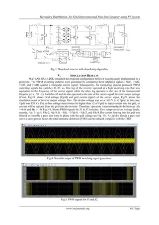
The output of the MPPT is the duty-cycle function. Fig.3. shown closed loop system. As the dc-link voltage Vdc
was controlled in the dc–ac seven level PWM inverter, the change of the duty cycle changes the voltage at the
output of the PV panels. A PID controller was implemented to keep the output voltage of the dc–dc boost
converter (Vdc) constant by comparing Vdc and Vdc ref and feeding the error into the PID controller, which
subsequently tries to reduce the error. In this way, the Vdc can be maintained at a constant value and at more
than √2 of Vgrid to inject power into the grid. To deliver energy to the grid, the frequency and phase of the PV
inverter must equal those of the grid; therefore, a grid synchronization method is needed. The sine lookup table
that generates reference current must be brought into phase with the grid voltage (Vgrid). For this, the grid
period and phase must be detected. The proposed inverter provides an analog zero-crossing detection circuit on
one of its input ports where the grid voltage is to be connected. The zero-crossing circuit then produces an in-
phase square-wave output that is fed into the digital I/O port on eZdsp board TMS320F2812. A PI algorithm
was used as the feedback current controller for the application. The current injected into the grid, also known as
grid current Igrid, was sensed and fed back to a comparator that compared it with the reference current Igridref .
Igridref is the result of the MPPT algorithm. The error from the comparison process of Igrid and Igridref was
fed into the PI controller. The output of the PI controller, also known as Vref, goes through an anti windup
process before being compared with the triangular wave to produce the switching signals for S1–S7 Eventually,
Vref becomes Vref1; Vref2; Vref3 and Vref4 can be derived from Vref1 by shifting the offset value, which was
equivalent to the amplitude of the triangular wave.
Secondary Distribution for Grid Interconnected Nine-level Inverter using PV system
www.iosrjournals.org 65 | Page
Fig.3. Nine-level inverter with closed-loop algorithm.
V. SIMULATION RESULTS
MATLAB SIMULINK simulated the proposed configuration before it was physically implemented in a
prototype. The PWM switching patterns were generated by comparing three reference signals (Vref1, Vref2,
Vref3, and Vref4) against a triangular carrier signal. Subsequently, the comparing process produced PWM
switching signals for switches S1–S7, as. One leg of the inverter operated at a high switching rate that was
equivalent to the frequency of the carrier signal, while the other leg operated at the rate of the fundamental
frequency (i.e., 50 Hz). Switches S5 and S6 also operated at the rate of the carrier signal. Inverter output voltage
(Vinv). Fig.10. shows Grid voltage (Vgrid) and grid current (Igrid) of the carrier signal. Fig.9. shows the
simulation result of inverter output voltage Vinv. The dc-bus voltage was set at 300 V (>√2Vgrid; in this case,
Vgrid was 120 V). The dc-bus voltage must always be higher than √2 of Vgrid to inject current into the grid, or
current will be injected from the grid into the inverter. Therefore, operation is recommended to be between Ma
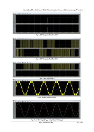
= 0.66 and Ma = 1.0. Fig.5-8. Shows PWM signals for S1 to S7 switches. Vinv comprises seven voltage levels,
namely, Vdc, 3Vdc/4, Vdc/2, Vdc/4, 0; −Vdc, −3Vdc/4, −Vdc/2, and Vdc/4.The current flowing into the grid was
filtered to resemble a pure sine wave in phase with the grid voltage see Fig. 10). As Igrid is almost a pure sine
wave at unity power factor, the total harmonic distortion (THD) can be reduced compared with the THD.
Fig.4. Simulink output of PWM switching signal generation.
Fig.5. PWM signals for S1 and S2.
Secondary Distribution for Grid Interconnected Nine-level Inverter using PV system
www.iosrjournals.org 66 | Page
Fig.6. PWM signals for S2 and S4.
Fig.7. PWM signals for S5 and S6.
Fig.8. PWM signal for S7.
Fig.9. Inverter output voltage.
Fig.10. Grid voltage (V grid) and grid current (I grid).
Secondary Distribution for Grid Interconnected Nine-level Inverter using PV system
www.iosrjournals.org 67 | Page
TABLE 2
COMPARISON OF THD IN DIFFERENT LEVELS
Sl. No. Levels Total Harmonic
Distortion (THD) in
%
Ripple current (A) Frequency
1. 3-level 8.0 1.92 50.00
2. 5-level 5.4 1.94 50.03
3. 7-level 3.9 2.48 50.00
4. 9-level 2.8 2.76 50.03
VI. CONCLUSION
Multilevel inverters offer improved output waveforms and lower THD. This paper has presented a
novel PWM switching scheme for the proposed multilevel inverter. It utilizes four reference signals and a
triangular carrier signal to generate PWM switching signals. The behavior of the proposed multilevel inverter
was analyzed in detail. By controlling the modulation index, the desired number of levels of the inverter’s
output voltage can be achieved. Table 2 shows the less THD in the nine-level inverter compared with that in the
seven- level, five-level and three level inverters is an attractive solution for grid-connected PV inverters.
REFERENCES
[1] M. Calais and V. G. Agelidis, ―Multilevel converters for single-phase grid connected photovoltaic systems—an overview,‖ in Proc.
IEEE Int. Symp. Ind. Electron. 1998, vol. 1, pp. 224–229.
[2] S. B. Kjaer, J. K. Pedersen, and F. Blaabjerg, ―A review of single-phase grid connected inverters for photovoltaic modules,‖ IEEE
Trans. Ind. Appl., vol. 41, no. 5, pp. 1292–1306, Sep./Oct. 2005.
[3] P. K. Hinga, T. Ohnishi, and T. Suzuki, ―A new PWM inverter for photovoltaic power generation system,‖ in Conf. Rec. IEEE
Power Electron. Spec. Conf., 1994, pp. 391–395.
[4] Y. Cheng, C. Qian, M. L. Crow, S. Pekarek, and S. Atcitty, ―A comparison of diode-clamped and cascaded multilevel converters for
a STATCOM with energy storage,‖ IEEE Trans. Ind. Electron., vol. 53, no. 5, pp. 1512– 1521, Oct. 2006.
[5] M. Saeedifard, R. Iravani, and J. Pou, ―A space vector modulation strategy for a back-to-back five-level HVDC converter system,‖
IEEE Trans. Ind. Electron., vol. 56, no. 2, pp. 452–466, Feb. 2009.
[6] S. Alepuz, S. Busquets-Monge, J. Bordonau, J. A. M. Velasco, C. A. Silva, J. Pontt, and J. Rodríguez, ―Control strategies based on
symmetrical components for grid-connected converters under voltage dips,‖ IEEE Trans. Ind. Electron., vol. 56, no. 6, pp. 2162–
2173, Jun. 2009.
[7] J. Rodríguez, J. S. Lai, and F. Z. Peng, ―Multilevel inverters: A survey of topologies, controls, and applications,‖ IEEE Trans. Ind.
Electron., vol. 49, no. 4, pp. 724–738, Aug. 2002.
[8] J. Rodriguez, S. Bernet, B. Wu, J. O. Pontt, and S. Kouro, ―Multilevel voltage-source-converter topologies for industrial medium-
voltage drives,‖ IEEE Trans. Ind. Electron., vol. 54, no. 6, pp. 2930–2945, Dec. 2007.
[9] M. M. Renge and H. M. Suryawanshi, ―Five-level diode clamped inverter to eliminate common mode voltage and reduce dv/dt in
medium voltage rating induction motor drives,‖ IEEE Trans. Power Electron., vol. 23, no. 4, pp. 1598–1160, Jul. 2008.
[10] E. Ozdemir, S. Ozdemir, and L. M. Tolbert, ―Fundamental-frequencymodulatedSix-level diode-clamped multilevel inverter for
three-phaseStand-alone photovoltaic system,‖ IEEE Trans. Ind. Electron., vol. 56, No. 11, pp. 4407–4415, Nov. 2009.
[11] R. Stala, S. Pirog, M. Baszynski, A. Mondzik, A. Penczek, J. Czekonski, and S. Gasiorek, ―Results of investigation of multicell
converters with balancing circuit—Part I,‖ IEEE Trans. Ind. Electron., vol. 56, no. 7, pp. 2610–2619, Jul. 2009.
[12] R. Stala, S. Pirog, M. Baszynski, A. Mondzik, A. Penczek, J. Czekonski, and S. Gasiorek, ―Results of investigation of multicell
converters with balancing circuit—Part II,‖ IEEE Trans. Ind. Electron., vol. 56, no. 7, pp. 2620–2628, Jul. 2009.
[13] P. Lezana, R. Aguilera, and D. E. Quevedo, ―Model predictive control of an asymmetric flying capacitor converter,‖ IEEE Trans.
Ind. Electron., vol. 56, no. 6, pp. 1839–1846, Jun. 2009.
[14] M. F. Escalante, J.-C. Vannier, and A. Arzandé, ―Flying capacitor multilevel inverters and DTC motor drive applications,‖ IEEE
Trans. Ind. Electron., vol. 49, no. 4, pp. 809–815, Aug. 2002.
[15] A. Shukla, A. Ghosh, and A. Joshi, ―Static shunt and series compensations of an SMIB system using flying capacitor multilevel
inverter,‖ IEEE Trans. Power Del., vol. 20, no. 4, pp. 2613–2622, Oct. 2005.
[16] J. Huang and K. A. Corzine, ―Extended operation of flying capacitor multilevel inverter,‖ IEEE Trans. Power Electron., vol. 21, no.
1, pp. 140– 147, Jan. 2006.
[17] F. Z. Peng, ―A generalized multilevel inverter topology with self voltage balancing,‖ IEEE Trans. Ind. Appl., vol. 37, no. 2, pp.
611–617, Mar./Apr. 2001.
[18] E. Villanueva, P. Correa, J. Rodríguez, andM. Pacas, ―Control of a singlephase cascaded H-bridge multilevel inverter for grid-
connected photovoltaic systems,‖ IEEE Trans. Ind. Electron., vol. 56, no. 11, pp. 4399– 4406, Nov. 2009.
[19] L. M. Tolbert, F. Z. Peng, T. Cunnyngham, and J. N. Chiasson, ―Charge balance control schemes for cascademultilevel converter in
hybrid electric vehicles,‖ IEEE Trans. Ind. Electron., vol. 49, no. 5, pp. 1058–1064, Oct. 2002.
[20] K. A. Corzine, M. W. Wielebski, F. Z. Peng, and J. Wang, ―Control of cascaded multilevel inverters,‖ IEEE Trans. Power
Electron., vol. 19, no. 3, pp. 732–738, May 2004.
[21] J. I. Leon, S. Vazquez, S. Kouro, L. G. Franquelo, J. M. Carrasco, and J. Rodriguez, ―Unidimensional modulation technique for
cascaded multilevel converters,‖ IEEE Trans. Ind. Electron., vol. 49, no. 5, pp. 1058– 1064, Oct. 2002.
[22] C.-C. Hua, C.-W. Wu and C.-W. Chuang, ―A digital predictive current control with improved sampled inductor current for cascaded
inverters,‖ IEEE Trans. Ind. Electron., vol. 56, no. 5, pp. 1718–1726, May 2009.
[23] S. Vazquez, J. I. Leon, L. G. Franquelo, J. J. Padilla, and J. M. Carrasco, ―DC-voltage-ratio control strategy for multilevel cascaded
converters fed with a single DC source,‖ IEEE Trans. Ind. Electron., vol. 56, no. 7, pp. 2513–2521, Jul. 2009.
[24] C. Cecati, F. Ciancetta, and P. Siano, ―A multilevel inverter for photovoltaic systems with fuzzy logic control,‖ IEEE Trans. Ind.
Electron., vol. 57, no. 12, pp. 4115–4125, Dec. 2010.
[25] G. Ceglia, V. Guzman, C. Sanchez, F. Ibanez, J. Walter, and M. I. Gimanez, ―A new simplified multilevel inverter topology for
DC–AC conversion,‖ IEEE Trans. Power Electron., vol. 21, no. 5, pp. 1311–1319, Sep. 2006.
Secondary Distribution for Grid Interconnected Nine-level Inverter using PV system
www.iosrjournals.org 68 | Page
[26] V. G. Agelidis, D. M. Baker, W. B. Lawrance, and C. V. Nayar, ―A multilevel PWMinverter topology for photovoltaic
applications,‖ in Proc. IEEE ISIE, Guimäes, Portugal, 1997, pp. 589–594.
[27] S. J. Park, F. S. Kang,M.H.Lee, and C. U. Kim, ―Anewsingle-phase fivelevel PWM inverter employing a deadbeat control scheme,‖
IEEE Trans. Power Electron., vol. 18, no. 3, pp. 831–843, May 2003.
[28] J. Selvaraj and N. A. Rahim, ―Multilevel inverter for grid-connected PV system employing digital PI controller,‖ IEEE Trans. Ind.
Electron., vol. 56, no. 1, pp. 149–158, Jan. 2009.
[29] N. A. Rahim and J. Selvaraj, ―Multi-string five-level inverter with novel PWM control scheme for PV application,‖ IEEE Trans.
Ind. Electron., vol. 57, no. 6, pp. 2111–2121, Jun. 2010.
[30] M. P. Kazmierkowski, R. Krishnan, and F. Blaabjerg, Control in Power Electronics Selected Problems. New York: Academic,
2002.

Secondary Distribution for Grid Interconnected Nine-level Inverter using PV system

  • 1.
    IOSR Journal ofElectrical and Electronics Engineering (IOSR-JEEE) e-ISSN: 2278-1676,p-ISSN: 2320-3331, Volume 6, Issue 3 (May. - Jun. 2013), PP 61-68 www.iosrjournals.org www.iosrjournals.org 61 | Page Secondary Distribution for Grid Interconnected Nine-level Inverter using PV system K. Hanumantha Rao1 , Nakeertha Suresh2 , Prof. D. Shobha Rani3 1, 2, 3 (Department of EEE, Vardhaman College of Engineering (Autonomous), JNTU Hyderabad, India) Abstract : This paper proposes a Secondary distribution (single phase) nine -level inverter for grid- connected photovoltaic systems, with a novel pulse width modulated (PWM) control scheme. F o u r reference signals that are identical to each other with an offset that is equivalent to the amplitude of the triangular carrier signal were used to generate the PWM signals. The inverter is capable of producing nine levels of output-voltage levels (Vdc , 3Vdc /4, Vdc /2,Vdc/4, 0, −Vdc , −3Vdc /4, −Vdc /2, Vdc/4) from the dc supply voltage. A digital proportional–integral current-control algorithm was implemented in a TMS320F2812 DSP to keep the current injected into the grid sinusoidal. The proposed system was verified through simulation and implemented in a prototype. Keywords - Grid connected, modulation index, multilevel inverter, photovoltaic (PV) system, pulse width modulated (PWM), total harmonic distortion (THD). I. INTRODUCTION The ever-increasing energy consumption, fossil fuels’ soaring costs and exhaustible nature, and worsening global environment have created a booming interest in renewable energy generation systems, one of which is photovoltaic. Such a system generates electricity by converting the Sun’s energy directly into electricity. Photovoltaic-generated energy can be delivered to power system networks through grid-connected inverters. A single-phase grid-connected inverter is usually used for residential or low-power applications of power ranges that are less than 10 kW. Types of single-phase grid-connected inverters have been investigated. A common topology of this inverter is full-bridge three-level. The three-level inverter can satisfy specifications through its very high switching, but it could also unfortunately increase switching losses, acoustic noise, and level of interference to other equipment. Improving its output waveform reduces its harmonic content and, hence, also the size of the filter used and the level of electromagnetic interference (EMI) generated by the inverter’s switching operation. Multilevel inverters are promising; they have nearly sinusoidal output-voltage waveforms, output current with better harmonic profile, less stressing of electronic components owing to decreased voltages, switching losses that are lower than those of conventional two-level inverters, a smaller filter size, and lower EMI, all of which make them cheaper, lighter, and more compact. Various topologies for multilevel inverters have been proposed over the years. Common ones are diode-clamped, flying capacitor or multi cell, cascaded H-bridge, and modified H-bridge multilevel. This paper recounts the development of a novel modified H-bridge single-phase multilevel inverter that has two diode embedded bidirectional switches and a novel pulse width modulated (PWM) technique. The topology was applied to a grid-connected photovoltaic system with considerations for a maximum-power-point tracker (MPPT) and a current-control algorithm. II. PROPOSED MULTILEVEL INVERTER The proposed single-phase nine-level inverter was developed from the seven-level inverter in. It comprises a single-phase conventional H-bridge inverter, two bidirectional switches, and a capacitor voltage divider formed by C1, C2, C3, and C4 as shown in Fig. 1. The modified H-bridge topology is significantly advantageous over other topologies, i.e., less power switch, power diodes, and less capacitors for inverters of the same number of levels. Photovoltaic (PV) arrays were connected to the inverter via a dc–dc boost converter. The power generated by the inverter is to be delivered to the power network, so the utility grid, rather than a load, was used. The dc–dc boost converter was required. The because the PV arrays had a voltage that was lower than the grid voltage. High dc bus voltages are necessary to ensure that power flows from the PV arrays to the grid. A filtering inductance Lf was used to filter the current injected into the grid. Proper switching of the inverter can produce seven output-voltage levels (Vdc, 3Vdc /4, Vdc /2, Vdc/4, 0, −Vdc, −3Vdc /4, −Vdc/2, Vdc/4) from the dc supply voltage.
  • 2.
    Secondary Distribution forGrid Interconnected Nine-level Inverter using PV system www.iosrjournals.org 62 | Page Fig. 1. Proposed single phase nine-level grid-connected inverter for photovoltaic systems. Fig. 2. Nine-level inverter for switching operation. The single-phase nine-level inverter was developed from the seven-level inverter as shown in Fig.1. It comprises a single-phase conventional H-bridge inverter, three bidirectional switches, and a capacitor voltage divider formed by C1, C2,C3 and C4, , as shown in Fig. 1. The modified H-bridge topology is significantly advantageous over other topologies, i.e., less power switch, power diodes, and less capacitor for inverters of the same number of levels. Photovoltaic (PV) arrays were connected to the inverter via a dc–dc boost converter. The power generated by the inverter is to be delivered to induction Motor. The dc–dc boost converter was required because the PV arrays had a voltage that was lower than the single-phase voltage. High dc bus voltages are necessary to ensure that power flows from the PV arrays to the single-phase induction motor. The LC-filter is modeled to obtain pure sine-wave and is given to drive a single-phase induction motor.. Proper switching of the inverter can produce nine- output-voltage-levels ( Vdc, 3 V d c /4, V d c /2, V d c /4, 0 ,-Vdc/4, -Vdc/2, -3Vdc/4, - Vdc) from the dc supply voltage. The proposed inverter’s operation can be divided into nine switching states. The required nine levels of output voltage were generated as follows. Maximum positive output (Vdc): S1 is ON; connecting the load positive terminal to Vdc, and S4 is ON, connecting the load negative terminal to ground. All other controlled switches are OFF; the voltage applied to the load terminals is Vdc. Three-fourth positive output (3Vdc/4): The bidirectional switch S5 is ON, connecting the load positive terminal, and S4 is ON, connecting the load negative terminal to ground. All other controlled switches are OFF; the voltage applied to the load terminals is 3Vdc/4. Half of the positive output (Vdc/2): The bidirectional switch S6 is ON, connecting the load positive terminal, and S4 is ON, connecting the load negative terminal to ground. All other controlled switches are OFF; the voltage applied to the load terminals is Vdc/2. One-fourth of the positive output (Vdc/4): The bidirectional switch S7 is ON, connecting the load positive terminal, and S4 is ON, connecting the load negative terminal to ground. All other controlled switches are OFF; the voltage applied to the load terminals is Vdc/4. Zero output: This level can be produced by two switching combinations; switches S3 and S4 are ON, or S1 andS2 are ON, and all other controlled switches are OFF; terminal ab is a short circuit, and the voltage applied to the load terminals is zero.
  • 3.
    Secondary Distribution forGrid Interconnected Nine-level Inverter using PV system www.iosrjournals.org 63 | Page One-fourth negative output (−Vdc/4): The bidirectional switch S5 is ON, connecting the load positive terminal, and S2 is ON, connecting the load negative terminal to Vdc. All other controlled switches are OFF; the voltage applied to the load terminals is −Vdc/4. Half of the negative output (−Vdc/2): The bidirectional switch S6 is ON, connecting the load positive terminal, and S2 is ON, connecting the load negative terminal to ground. All other controlled switches are OFF; the voltage applied to the load terminals is −Vdc/2 Three-fourth negative output (−3Vdc/4): The bidirectional switch S7 is ON, connecting the load positive terminal, and S2 is ON, connecting the load negative terminal to ground. All other controlled switches are OFF; the voltage applied to the load terminals is −3Vdc/4. Maximum negative output (−Vdc): S2 is ON; connecting the load negative terminal to Vdc, and S3 is ON, connecting the load positive terminal to ground. All other controlled switches are OFF; the voltage applied to the load terminals is −Vdc. Table I shows the switching combinations that generated the nine output-voltage levels (Vdc, 3Vdc/4, Vdc/2, Vdc/4, 0,-Vdc/4, -Vdc/2, -3Vdc/4, - Vdc) TABLE 1 Out Put Voltage According To The Switches On Off Vo S1 S2 S3 S4 S5 S6 S7 Vdc On Off Off On Off Off Off 3Vdc/4 Off Off Off On On Off Off Vdc/2 Off Off Off On Off On Off Vdc/4 Off Off Off On Off Off On 0 Off Off On On Off Off Off -Vdc/4 Off On Off Off On Off Off -Vdc/2 Off On Off Off Off On Off -3Vdc/4 Off On Off Off Off Off On -Vdc Off On On Off Off Off Off III. PWM TECHNIQUE A novel PWM modulation technique was introduced to generate the PWM switching signals. Four reference signals (Vref1, Vref2, Vref3, and Vref4) were compared with a carrier signal (Vcarrier). The reference signals had the same frequency and amplitude and were in phase with an offset value that was equivalent to the amplitude of the carrier signal. The reference signals were each compared with the carrier signal. If Vref1 had exceeded the peak amplitude of Vcarrier, Vref2 was com- pared with Vcarrier until it had exceeded the peak amplitudeof Vcarrier.Then, onward, Vref3 would take charge and would be compared with Vcarrier until it had exceeded the peak amplitude of Vcarrier. Then Vref4 would take the charge to reached zero. Once Vref4 had reached zero, Vref3 would be compared until it reached zero. Then, onward, Vref2 would take charge to reached zero; Vref1 would be compared with Vcarrier. The resulting switching pattern. Switches S1, S3, S5, S 6 , a n d S7 would be switching at the rate of the carrier signal frequency, whereas S2 and S4 would operate at a frequency that was equivalent to the fundamental frequency.Fig.2 shown signalgeneration.
  • 4.
    Secondary Distribution forGrid Interconnected Nine-level Inverter using PV system www.iosrjournals.org 64 | Page Fig.2. PWM Switching signal generator. IV. CLOSED LOOP CONTROL SYSTEM The control system comprises a MPPT algorithm, a dc-bus voltage controller, reference-current generation and a current controller. The two main tasks of the control system are maximization of the energy transferred from the PV arrays to the grid, and generation of a sinusoidal current with minimum harmonic distortion, also under the presence of grid voltage harmonics. The proposed inverter utilizes the perturb-and- observe (P&O) algorithm for its wide usage in MPPT owing to its simple structure and requirement of only a few measured parameters. It periodically perturbs (i.e., increment or decrement) the array terminal voltage and compares the PV output power with that of the previous perturbation cycle. If the power was increasing, the perturbation would continue in the same direction in the next cycle; otherwise, the direction would be reversed. This means that the array terminal voltage is perturbed every MPPT cycle; therefore, when the MPP is reached, the P&O algorithm will oscillate around it. The P&O algorithm was implemented in the dc–dc boost converter. The output of the MPPT is the duty-cycle function. Fig.3. shown closed loop system. As the dc-link voltage Vdc was controlled in the dc–ac seven level PWM inverter, the change of the duty cycle changes the voltage at the output of the PV panels. A PID controller was implemented to keep the output voltage of the dc–dc boost converter (Vdc) constant by comparing Vdc and Vdc ref and feeding the error into the PID controller, which subsequently tries to reduce the error. In this way, the Vdc can be maintained at a constant value and at more than √2 of Vgrid to inject power into the grid. To deliver energy to the grid, the frequency and phase of the PV inverter must equal those of the grid; therefore, a grid synchronization method is needed. The sine lookup table that generates reference current must be brought into phase with the grid voltage (Vgrid). For this, the grid period and phase must be detected. The proposed inverter provides an analog zero-crossing detection circuit on one of its input ports where the grid voltage is to be connected. The zero-crossing circuit then produces an in- phase square-wave output that is fed into the digital I/O port on eZdsp board TMS320F2812. A PI algorithm was used as the feedback current controller for the application. The current injected into the grid, also known as grid current Igrid, was sensed and fed back to a comparator that compared it with the reference current Igridref . Igridref is the result of the MPPT algorithm. The error from the comparison process of Igrid and Igridref was fed into the PI controller. The output of the PI controller, also known as Vref, goes through an anti windup process before being compared with the triangular wave to produce the switching signals for S1–S7 Eventually, Vref becomes Vref1; Vref2; Vref3 and Vref4 can be derived from Vref1 by shifting the offset value, which was equivalent to the amplitude of the triangular wave.
  • 5.
    Secondary Distribution forGrid Interconnected Nine-level Inverter using PV system www.iosrjournals.org 65 | Page Fig.3. Nine-level inverter with closed-loop algorithm. V. SIMULATION RESULTS MATLAB SIMULINK simulated the proposed configuration before it was physically implemented in a prototype. The PWM switching patterns were generated by comparing three reference signals (Vref1, Vref2, Vref3, and Vref4) against a triangular carrier signal. Subsequently, the comparing process produced PWM switching signals for switches S1–S7, as. One leg of the inverter operated at a high switching rate that was equivalent to the frequency of the carrier signal, while the other leg operated at the rate of the fundamental frequency (i.e., 50 Hz). Switches S5 and S6 also operated at the rate of the carrier signal. Inverter output voltage (Vinv). Fig.10. shows Grid voltage (Vgrid) and grid current (Igrid) of the carrier signal. Fig.9. shows the simulation result of inverter output voltage Vinv. The dc-bus voltage was set at 300 V (>√2Vgrid; in this case, Vgrid was 120 V). The dc-bus voltage must always be higher than √2 of Vgrid to inject current into the grid, or current will be injected from the grid into the inverter. Therefore, operation is recommended to be between Ma = 0.66 and Ma = 1.0. Fig.5-8. Shows PWM signals for S1 to S7 switches. Vinv comprises seven voltage levels, namely, Vdc, 3Vdc/4, Vdc/2, Vdc/4, 0; −Vdc, −3Vdc/4, −Vdc/2, and Vdc/4.The current flowing into the grid was filtered to resemble a pure sine wave in phase with the grid voltage see Fig. 10). As Igrid is almost a pure sine wave at unity power factor, the total harmonic distortion (THD) can be reduced compared with the THD. Fig.4. Simulink output of PWM switching signal generation. Fig.5. PWM signals for S1 and S2.
  • 6.
    Secondary Distribution forGrid Interconnected Nine-level Inverter using PV system www.iosrjournals.org 66 | Page Fig.6. PWM signals for S2 and S4. Fig.7. PWM signals for S5 and S6. Fig.8. PWM signal for S7. Fig.9. Inverter output voltage. Fig.10. Grid voltage (V grid) and grid current (I grid).
  • 7.
    Secondary Distribution forGrid Interconnected Nine-level Inverter using PV system www.iosrjournals.org 67 | Page TABLE 2 COMPARISON OF THD IN DIFFERENT LEVELS Sl. No. Levels Total Harmonic Distortion (THD) in % Ripple current (A) Frequency 1. 3-level 8.0 1.92 50.00 2. 5-level 5.4 1.94 50.03 3. 7-level 3.9 2.48 50.00 4. 9-level 2.8 2.76 50.03 VI. CONCLUSION Multilevel inverters offer improved output waveforms and lower THD. This paper has presented a novel PWM switching scheme for the proposed multilevel inverter. It utilizes four reference signals and a triangular carrier signal to generate PWM switching signals. The behavior of the proposed multilevel inverter was analyzed in detail. By controlling the modulation index, the desired number of levels of the inverter’s output voltage can be achieved. Table 2 shows the less THD in the nine-level inverter compared with that in the seven- level, five-level and three level inverters is an attractive solution for grid-connected PV inverters. REFERENCES [1] M. Calais and V. G. Agelidis, ―Multilevel converters for single-phase grid connected photovoltaic systems—an overview,‖ in Proc. IEEE Int. Symp. Ind. Electron. 1998, vol. 1, pp. 224–229. [2] S. B. Kjaer, J. K. Pedersen, and F. Blaabjerg, ―A review of single-phase grid connected inverters for photovoltaic modules,‖ IEEE Trans. Ind. Appl., vol. 41, no. 5, pp. 1292–1306, Sep./Oct. 2005. [3] P. K. Hinga, T. Ohnishi, and T. Suzuki, ―A new PWM inverter for photovoltaic power generation system,‖ in Conf. Rec. IEEE Power Electron. Spec. Conf., 1994, pp. 391–395. [4] Y. Cheng, C. Qian, M. L. Crow, S. Pekarek, and S. Atcitty, ―A comparison of diode-clamped and cascaded multilevel converters for a STATCOM with energy storage,‖ IEEE Trans. Ind. Electron., vol. 53, no. 5, pp. 1512– 1521, Oct. 2006. [5] M. Saeedifard, R. Iravani, and J. Pou, ―A space vector modulation strategy for a back-to-back five-level HVDC converter system,‖ IEEE Trans. Ind. Electron., vol. 56, no. 2, pp. 452–466, Feb. 2009. [6] S. Alepuz, S. Busquets-Monge, J. Bordonau, J. A. M. Velasco, C. A. Silva, J. Pontt, and J. Rodríguez, ―Control strategies based on symmetrical components for grid-connected converters under voltage dips,‖ IEEE Trans. Ind. Electron., vol. 56, no. 6, pp. 2162– 2173, Jun. 2009. [7] J. Rodríguez, J. S. Lai, and F. Z. Peng, ―Multilevel inverters: A survey of topologies, controls, and applications,‖ IEEE Trans. Ind. Electron., vol. 49, no. 4, pp. 724–738, Aug. 2002. [8] J. Rodriguez, S. Bernet, B. Wu, J. O. Pontt, and S. Kouro, ―Multilevel voltage-source-converter topologies for industrial medium- voltage drives,‖ IEEE Trans. Ind. Electron., vol. 54, no. 6, pp. 2930–2945, Dec. 2007. [9] M. M. Renge and H. M. Suryawanshi, ―Five-level diode clamped inverter to eliminate common mode voltage and reduce dv/dt in medium voltage rating induction motor drives,‖ IEEE Trans. Power Electron., vol. 23, no. 4, pp. 1598–1160, Jul. 2008. [10] E. Ozdemir, S. Ozdemir, and L. M. Tolbert, ―Fundamental-frequencymodulatedSix-level diode-clamped multilevel inverter for three-phaseStand-alone photovoltaic system,‖ IEEE Trans. Ind. Electron., vol. 56, No. 11, pp. 4407–4415, Nov. 2009. [11] R. Stala, S. Pirog, M. Baszynski, A. Mondzik, A. Penczek, J. Czekonski, and S. Gasiorek, ―Results of investigation of multicell converters with balancing circuit—Part I,‖ IEEE Trans. Ind. Electron., vol. 56, no. 7, pp. 2610–2619, Jul. 2009. [12] R. Stala, S. Pirog, M. Baszynski, A. Mondzik, A. Penczek, J. Czekonski, and S. Gasiorek, ―Results of investigation of multicell converters with balancing circuit—Part II,‖ IEEE Trans. Ind. Electron., vol. 56, no. 7, pp. 2620–2628, Jul. 2009. [13] P. Lezana, R. Aguilera, and D. E. Quevedo, ―Model predictive control of an asymmetric flying capacitor converter,‖ IEEE Trans. Ind. Electron., vol. 56, no. 6, pp. 1839–1846, Jun. 2009. [14] M. F. Escalante, J.-C. Vannier, and A. Arzandé, ―Flying capacitor multilevel inverters and DTC motor drive applications,‖ IEEE Trans. Ind. Electron., vol. 49, no. 4, pp. 809–815, Aug. 2002. [15] A. Shukla, A. Ghosh, and A. Joshi, ―Static shunt and series compensations of an SMIB system using flying capacitor multilevel inverter,‖ IEEE Trans. Power Del., vol. 20, no. 4, pp. 2613–2622, Oct. 2005. [16] J. Huang and K. A. Corzine, ―Extended operation of flying capacitor multilevel inverter,‖ IEEE Trans. Power Electron., vol. 21, no. 1, pp. 140– 147, Jan. 2006. [17] F. Z. Peng, ―A generalized multilevel inverter topology with self voltage balancing,‖ IEEE Trans. Ind. Appl., vol. 37, no. 2, pp. 611–617, Mar./Apr. 2001. [18] E. Villanueva, P. Correa, J. Rodríguez, andM. Pacas, ―Control of a singlephase cascaded H-bridge multilevel inverter for grid- connected photovoltaic systems,‖ IEEE Trans. Ind. Electron., vol. 56, no. 11, pp. 4399– 4406, Nov. 2009. [19] L. M. Tolbert, F. Z. Peng, T. Cunnyngham, and J. N. Chiasson, ―Charge balance control schemes for cascademultilevel converter in hybrid electric vehicles,‖ IEEE Trans. Ind. Electron., vol. 49, no. 5, pp. 1058–1064, Oct. 2002. [20] K. A. Corzine, M. W. Wielebski, F. Z. Peng, and J. Wang, ―Control of cascaded multilevel inverters,‖ IEEE Trans. Power Electron., vol. 19, no. 3, pp. 732–738, May 2004. [21] J. I. Leon, S. Vazquez, S. Kouro, L. G. Franquelo, J. M. Carrasco, and J. Rodriguez, ―Unidimensional modulation technique for cascaded multilevel converters,‖ IEEE Trans. Ind. Electron., vol. 49, no. 5, pp. 1058– 1064, Oct. 2002. [22] C.-C. Hua, C.-W. Wu and C.-W. Chuang, ―A digital predictive current control with improved sampled inductor current for cascaded inverters,‖ IEEE Trans. Ind. Electron., vol. 56, no. 5, pp. 1718–1726, May 2009. [23] S. Vazquez, J. I. Leon, L. G. Franquelo, J. J. Padilla, and J. M. Carrasco, ―DC-voltage-ratio control strategy for multilevel cascaded converters fed with a single DC source,‖ IEEE Trans. Ind. Electron., vol. 56, no. 7, pp. 2513–2521, Jul. 2009. [24] C. Cecati, F. Ciancetta, and P. Siano, ―A multilevel inverter for photovoltaic systems with fuzzy logic control,‖ IEEE Trans. Ind. Electron., vol. 57, no. 12, pp. 4115–4125, Dec. 2010. [25] G. Ceglia, V. Guzman, C. Sanchez, F. Ibanez, J. Walter, and M. I. Gimanez, ―A new simplified multilevel inverter topology for DC–AC conversion,‖ IEEE Trans. Power Electron., vol. 21, no. 5, pp. 1311–1319, Sep. 2006.
  • 8.
    Secondary Distribution forGrid Interconnected Nine-level Inverter using PV system www.iosrjournals.org 68 | Page [26] V. G. Agelidis, D. M. Baker, W. B. Lawrance, and C. V. Nayar, ―A multilevel PWMinverter topology for photovoltaic applications,‖ in Proc. IEEE ISIE, Guimäes, Portugal, 1997, pp. 589–594. [27] S. J. Park, F. S. Kang,M.H.Lee, and C. U. Kim, ―Anewsingle-phase fivelevel PWM inverter employing a deadbeat control scheme,‖ IEEE Trans. Power Electron., vol. 18, no. 3, pp. 831–843, May 2003. [28] J. Selvaraj and N. A. Rahim, ―Multilevel inverter for grid-connected PV system employing digital PI controller,‖ IEEE Trans. Ind. Electron., vol. 56, no. 1, pp. 149–158, Jan. 2009. [29] N. A. Rahim and J. Selvaraj, ―Multi-string five-level inverter with novel PWM control scheme for PV application,‖ IEEE Trans. Ind. Electron., vol. 57, no. 6, pp. 2111–2121, Jun. 2010. [30] M. P. Kazmierkowski, R. Krishnan, and F. Blaabjerg, Control in Power Electronics Selected Problems. New York: Academic, 2002.