Download to read offline
![A R N Rao et al Int. Journal of Engineering Research and Applications
ISSN : 2248-9622, Vol. 3, Issue 6, Nov-Dec 2013, pp.2053-2059
RESEARCH ARTICLE
www.ijera.com
OPEN ACCESS
Three-Phase Nine-Level Inverter for Photovoltaic System with
Induction Motor
A R Neelakanteswara Rao1, T Nagadurga2
1
2
M.TECH Scholar, Dept of EEE, GEC Gudlavalleru, AP, India
Assistant Professor, Dept. of EEE, GEC Gudlavalleru, AP, India
Abstract
Electrical power play a vital rule in 21th century, but non-conventional sources scale down day by day. Not only
that concern for the environmental pollution around the world, so now a day’s photovoltaic (PV) power systems
are getting more and more widespread with the increase in the energy demand. This paper proposed a three
phase nine level inverter with voltage control method using semiconductor power devices for three phase
induction motor in order to achieve a smooth, continuous and low total harmonics distortion (THD) waveforms.
The proposed inverter system gives better voltage regulation, smooth results and efficiency compared to multilevel inverters. The inverter is capable of producing nine levels of output voltage levels (Vdc, 3Vdc/4,Vdc/2,
Vdc/4, 0, -Vdc/4, -Vdc/2, -3Vdc/4, -Vdc) The proposed inverter was verified by using simulation of
MATLAB/SIMULINK software.
Index terms: Photovoltaic (PV) system, multi-level inverter, semiconductor power devices, THD, induction
motor.
I.
Introduction
As the world is concerned with the fossil fuel
exhaustion and environmental problem caused by
conventional power generation, particularly solar have
become very popular and demanding. PV sources are
used in many applications because they have
advantage of being maintenance and pollution free. It
is used to convert the dc power from solar module to
ac power to feed into load.
The proposed three phase nine level inverter
is very suitable to PV module with induction motor
load, because of compare to common three phase
multi-level inverter have high switching, but it could
also unfortunately increase switching losses, acoustic
noise, and level of interference to other equipment.
Improving its output waveform reduces its harmonic
content and, hence, also the size of the filter used and
the level of electromagnetic interference (EMI)
generated by the inverter’s switching operation.
This paper developed a modified H-bridge
single-phase multilevel inverter that has two diode
embedded bidirectional switches. Coming to three
phase proposed inverter required 21 switches
(IGBT’s) and six diode embedded bidirectional
switches, but in common three phase multi-level
inverter required 48 switches (IGBT’s). So this
topology have reduces a switching loss and high
efficiency. A boost converter (step-up DC-DC) used
in paper for high voltage before proposed inverter; this
topology was applied to three phase asynchronous
machine photovoltaic system with considerations for
voltage control pulse generator.
www.ijera.com
II.
Photovoltaic System (PV)
A solar cell basically is a p-n semiconductor
junction. When exposed to light, a current
proportional to solar irradiance is generated. Standard
simulation tools utilize the approximate diode
equivalent circuit shown in Fig. 1 in order to simulate
all electric circuits that contain diode. The circuit
consists of Ron in series with voltage source Von. PVs
generate electric power when illuminated by sunlight
or artificial light, the absorption of photons of energy
greater than the band-gap energy of the semiconductor
promotes electrons from the valence band to the
conduction band, creating hole-electron pairs
throughout the illuminated part of the semiconductor.
These electrons and holes pairs will flow in opposite
directions across the junction thereby creating DC
power.
Figure 1: circuit model of PV cell.
2.1 Mathematical Model:
The equation [1] & [2] that are used to solve
the mathematical model of the solar cell based on
simple equivalent circuit shown in Fig. 1, are given
below;
2053 | P a g e](https://image.slidesharecdn.com/lz3620532059-140101225823-phpapp02/85/Lz3620532059-1-320.jpg)

![A R N Rao et al Int. Journal of Engineering Research and Applications
ISSN : 2248-9622, Vol. 3, Issue 6, Nov-Dec 2013, pp.2053-2059
was equivalent to the fundamental frequency. For one
cycle of the fundamental frequency, the proposed
inverter operated through six modes. The per unit
output-voltage signal for one cycle.
www.ijera.com
change of the duty cycle changes the voltage at the
output of the PV panels. A PID controller was
implemented to keep the output voltage of the dc–dc
boost converter (Vdc) constant by comparing Vdc and
Vdc ref and feeding the error into the PID controller,
which subsequently tries to reduce the error. In this
way, the Vdc can be maintained.
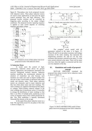
Figure 4: Seven-level output voltage (Vab) and
switching angles.
Figure 6: Simulation of pwm switching sequence.
Figure 5: Seven-level inverter with closed-loop
control algorithm
2.4 control system
The control system comprises a MPPT
algorithm, a dc-bus voltage controller, referencecurrent generation, and a current controller. The two
main tasks of the control system are maximization of
the energy transferred from the PV arrays to the grid,
and generation of a sinusoidal current with minimum
harmonic distortion, also under the presence of grid
voltage harmonics. The proposed inverter utilizes the
perturb-and-observe (P&O) algorithm for its wide
usage in MPPT owing to its simple structure and
requirement of only a few measured parameters. It
periodically perturbs (i.e., increment or decrement) the
array terminal voltage and compares the PV output
power with that of the previous perturbation cycle. If
the power was increasing, the perturbation would
continue in the same direction in the next cycle;
otherwise, the direction would be reversed. This
means that the array terminal voltage is perturbed
every MPPT cycle; therefore, when the MPP is
reached, the P&O algorithm will oscillate around it.
The P&O algorithm was implemented in the dc–dc
boost converter. The output of the MPPT is the dutycycle function. As the dc-link voltage Vdc was
controlled in the dc–ac seven level PWM inverter; the
www.ijera.com
For Ma that is equal to, or less than, 0.33,
only the lower reference wave (Vref3) is compared
with the triangular carrier signal. The inverter’s
behaviour is similar to that of a conventional fullbridge three-level PWM inverter. However, if Ma is
more than 0.33 and less than 0.66, only Vref2 and
Vref3 reference signals are compared with the
triangular carrier wave. The output voltage consists of
five dc-voltage levels. The modulation index is set to
be more than 0.66 for seven levels of output voltage to
be produced. Three reference signals have to be
compared with the triangular carrier signal to produce
switching signals for the switches.
Figure 7: Simulation circuit of Seven-level inverter
with closed-loop control algorithm
III.
Single-Phase Proposed Inverter
The proposed single-phase nine-level inverter
was developed from the five-level inverter in [12]. It
comprises a single-phase conventional H-bridge
2055 | P a g e](https://image.slidesharecdn.com/lz3620532059-140101225823-phpapp02/85/Lz3620532059-3-320.jpg)


![A R N Rao et al Int. Journal of Engineering Research and Applications
ISSN : 2248-9622, Vol. 3, Issue 6, Nov-Dec 2013, pp.2053-2059
[2]
[3]
[4]
[5]
Figure 21: THD result for nine-levels of output
voltage.
The
THD
measurement
of
Fig.19
corresponds to the waveform of Fig. 20, while the
THD measurements correspond to the waveforms of
respectively. Comparing all two THD measurements,
the nine-level inverter produced the lowest THD
compared with the seven-level inverter. This proves
that, as the level increases, the THD reduces.
Table5: total harmonic distortion different levels
Inverter level
THD
Seven level
22.13%
Nine level
18.63%
[6]
[7]
[8]
Three phase nine-level inverter output voltage and
current as shown in figure 17. This proposed inverter
output applied to induction motor of rating is 400V,
50Hz, below 1500RPM, and load torque 10. Induction
motor results shown in figure 18 and 19, in figure 18
shown rotor speed 1460RPM and Electromagnetic
torque; in figure 19 shown rotor current and stator
current. Finally THD in circuit 18%, this proposed
topology is very high efficiency and economic.
[9]
[10]
V.
Conclusion
This paper presents a new three phase ninelevel inverter with reduced switches compare to
common multi level inverter. Multilevel inverters
offer improved output waveforms and lower THD. In
this topology less THD in the nine-level inverter
compared with that in the seven-level inverters is
connected PV inverters. This inverter provided to
induction motor with smooth output and better
voltage. Switching loss reduce in this topology than
the common three phase multi-level-inverter.
References
[1]
M. Calais and V. G. Agelidis, ―Multilevel
converters for single-phase grid connected
photovoltaic systems—An overview,‖ in Proc.
www.ijera.com
[11]
[12]
www.ijera.com
IEEE Int. Symp. Ind. Electron., 1998, vol. 1, pp.
224–229.
S. B. Kjaer, J. K. Pedersen, and F. Blaabjerg,
―A review of single-phase grid connected
inverters for photovoltaic modules,‖ IEEE
Trans. Ind. Appl., vol. 41, no. 5, pp. 1292–1306,
Sep./Oct. 2005.
P. K. Hinga, T. Ohnishi, and T. Suzuki, ―A new
PWM inverter for photovoltaic power
generation system,‖ in Conf. Rec. IEEE Power
Electron. Spec. Conf., 1994, pp. 391–395.
Y. Cheng, C. Qian, M. L. Crow, S. Pekarek,
and S. Atcitty, ―A comparison of diodeclamped and cascaded multilevel converters for
a STATCOM with energy storage,‖ IEEE
Trans. Ind. Electron., vol. 53, no. 5, pp. 1512–
1521, Oct. 2006.
M. Saeedifard, R. Iravani, and J. Pou, ―A space
vector modulation strategy for a back-to-back
five-level HVDC converter system,‖ IEEE
Trans. Ind. Electron., vol. 56, no. 2, pp. 452–
466, Feb. 2009.
S. Alepuz, S. Busquets-Monge, J. Bordonau, J.
A. M. Velasco, C. A. Silva, J. Pontt, and J.
Rodríguez, ―Control strategies based on
symmetrical components for grid-connected
converters under voltage dips,‖ IEEE Trans.
Ind. Electron., vol. 56, no. 6, pp. 2162–2173,
Jun. 2009.
J. Rodríguez, J. S. Lai, and F. Z. Peng,
―Multilevel inverters: A survey of topologies,
controls, and applications,‖ IEEE Trans. Ind.
Electron., vol. 49, no. 4, pp. 724–738, Aug.
2002.
J. Rodriguez, S. Bernet, B. Wu, J. O. Pontt, and
S. Kouro, ―Multilevel voltage-source-converter
topologies for industrial medium-voltage
drives,‖ IEEE Trans. Ind. Electron., vol. 54, no.
6, pp. 2930–2945, Dec. 2007.
M. M. Renge and H. M. Suryawanshi, ―Fivelevel diode clamped inverterto eliminate
common mode voltage and reduce dv/dt in
medium voltagerating induction motor drives,‖
IEEE Trans. Power Electron., vol. 23, no. 4, pp.
1598–1160, Jul. 2008.
E. Ozdemir, S. Ozdemir, and L. M. Tolbert,
―Fundamental-frequencymodulatedsix-level
diode-clamped multilevel inverter for threephasestand-alone photovoltaic system,‖ IEEE
Trans. Ind. Electron., vol. 56, no. 11, pp. 4407–
4415, Nov. 2009.
P. Lezana, R. Aguilera, and D. E. Quevedo,
―Model predictive controlof an asymmetric
flying capacitor converter,‖ IEEE Trans. Ind.
Electron., vol. 56, no. 6, pp. 1839–1846, Jun.
2009.
G. Ceglia, V. Guzman, C. Sanchez, F. Ibanez, J.
Walter, and M. I. Gimanez, ―A new simplified
multilevel inverter topology for DC–AC
conversion,‖ IEEE Trans. Power Electron., vol.
21, no. 5, pp. 1311–1319, Sep. 2006.
2059 | P a g e](https://image.slidesharecdn.com/lz3620532059-140101225823-phpapp02/85/Lz3620532059-7-320.jpg)

The document discusses the development of a three-phase nine-level inverter designed for photovoltaic systems to efficiently drive induction motors. It highlights the inverter's capability to reduce total harmonic distortion (THD) while achieving smooth voltage regulation through a modified H-bridge topology and a dc-dc boost converter. Simulations in MATLAB/Simulink demonstrate the inverter's performance, showcasing its advantages over traditional multilevel inverters.


![6.[36 45]seven level modified cascaded inverter for induction motor drive app...](https://cdn.slidesharecdn.com/ss_thumbnails/6-36-45sevenlevelmodifiedcascadedinverterforinductionmotordriveapplications-111118181646-phpapp02-thumbnail.jpg?width=640&height=640&fit=bounds)