Download to read offline
![International Journal of Engineering Research and Development
e-ISSN: 2278-067X, p-ISSN: 2278-800X, www.ijerd.com
Volume 9, Issue 11 (February 2014), PP. 50-56
50
Single Phase Multilevel Inverter for AC Motor
Amrita Mariam Varghese1
, Eldhose K.A.2
, Ninu Joy3
1
P.G. Student,Mar Athanasius College of Engineering,kothamangalam,kerala
2,3
Assistant. Professor, Mar Athanasius College of Engineering,kothamangalam,kerala
Abstract:-As the demand for electrical energy is increasing, renewable energy sources has come into popularity
especially photovoltaic systems (PV). PV can act as a voltage source which is feeding a power circuit. This
study proposes a single phase multilevel inverter topology fed from a PV panel with a multicarrier phase
disposition sinusoidal pulse width modulation scheme (PWM) for the generation of gate signals for power
switches. Desired number of output levels: 3, 5, 7 and 9 is obtained by controlling modulation index. The
proposed inverter configuration was subjected to an R-L load. An LC filter is modelled to obtain pure sine wave
output and it‟s given to the load. %THD value for output current and voltage of the proposed configuration is
determined. Simulation has been carried out to study the performance of the proposed topology in
MATLAB/SIMULINK environment. Simulation results analysed and results presented for circuit.
Keywords:- Photovoltaic (PV), multilevel inverter, PWM, THD
I. INTRODUCTION
The ever increasing energy consumption has created a booming interest in renewable energy generation
systems, one of which is photovoltaic. Such a system generates electricity by converting the sun‟s energy
directly into electricity. Energy generated by photovoltaic can be delivered to drive electrical machines through
inverters. Multilevel inverters has been developed due to the increase in power level of industrial applications,
especially high power application. The topologies can be able to handle voltage/power in range of KV/MW.
Multilevel starts with a three level inverter introduced by Nabe. By increasing the number of levels the output
voltage has more steps generating a staircase waveform. Conventional multilevel inverters include diode
clamped, flying capacitor[1], cascaded H bridge (CHB).
This paper presents a new topology of a cascaded multilevel inverter fed by a photovoltaic (PV)
module that has less switches compared to the conventional topologies and has higher number of output levels.
By making use of appropriate PWM techniques, a multilevel inverter with lower THD can be designed that
would be useful for the design of a more compact filter. The proposed topology is similar to a CHB inverter
configuration with a difference that in each H-bridge an auxiliary/clamping/bidirectional switch is provided to
improve the overall harmonic profile of the output waveforms. Analysis of Operating principles and switching
functions are carried out and simulation results are presented.
II. PROPOSED CIRCUIT CONFIGURATION
The block diagram of the single-phase PV fed inverter is shown in fig.1. The PV module is connected
to the input of inverter as the source. The power generated by inverter is delivered to the load. A dc-dc boost
converter was required because the PV arrays have a lower voltage than the single phase voltage. The LC filter
is modelled to obtain pure sine – wave as output and is given to the load. Proper switching of the inverter can
produce nine output voltage levels: Vs/2, Vs, 3Vs/2, 2Vs,0, -Vs/2, -Vs,-3Vs/2, -2Vs. The auxiliary switches
should be properly switched depending on the direction of current.
Fig.1: Block diagram of the proposed circuit](https://image.slidesharecdn.com/g09115056-140322024246-phpapp01/85/International-Journal-of-Engineering-Research-and-Development-1-320.jpg)
![Single Phase Multilevel Inverter for AC Motor
51
A. PV Array Model and Boost Converter
The optimum power of the PV is useful for any purposes. Due to the various level of insolation, the
power output of the PV varies instantly. The overall output of PV depends on the number of cellsin the array,
the total power is the contribution of each cell. So, by calculating the output of one cell, we may calculate the
total output. The Fig .2 shows the equivalent circuit of a PV cell.
Fig.2: Equivalent circuit of a PV cell
Using equivalent circuit, the nonlinear Vpv-Ipv characteristics of PV module is:
Vpv=
1
λ
ln(
Isc –Ipv +IO
Io
) - RsIpv
Where Iscis the cell short-circuit current, Io is the reverse saturation current, Rsis the series cell
resistance, and λ is a constant coefficient and depends upon the cell material. Equation expresses a nonlinear
relation between voltage current characteristic of a PV module. The PV array is formed by the combination of
many PV cells connected in series and parallel fashion to provide the desired value of output voltage and
current. This PV array exhibits a nonlinear insolation-dependent V-I characteristic, mathematically expressed
[2,3]consisting of Ns cells in series and Np cells in parallel as
𝑉𝐴 = −IA(
𝑁 𝑆
𝑁 𝑃
)+(
𝑁 𝑆
𝜆
) ln{1 +
NpIph −Io
NpIo
}
Fig.3: SIMULINK model of a PV array and Boost converter
Fig.4:Input voltage to the multilevel inverter
τ = (q/AKT); q is the electric charge; A is the completion factor; K is the boltzmann‟s constant; T is the
absolute temperature; Rs is the cell series resistance; Iph is the current; Io is the cell reverse saturation current;
IA and VA are solar cell array current and voltage.](https://image.slidesharecdn.com/g09115056-140322024246-phpapp01/85/International-Journal-of-Engineering-Research-and-Development-2-320.jpg)
![Single Phase Multilevel Inverter for AC Motor
52
Boost converter is connected to the output of the PV module [4].A dc-dc boost converter is added to
obtain the single phase voltage required by electric machines as the PV arrays have a lower voltage.Fig.3.shows
the SIMULINK model of a PV module withboost converter and fig.4 shows the output of the above model.
B. Multilevel Inverter Topology
A single phase nine level inverter was developed from the five- level inverter [10] as shown in fig.5. It
comprises of a two single phase conventional H-bridge [7.8,9], two bidirectional switches and a capacitor
voltage divider formed by C1,C2,C3,C4 as shown in fig.5. High power semiconductor devices such as IGBT or
GTO transistors are used as switches. Turning ON of switches permits the addition of capacitor voltages and
generates high voltage at the output. For an n- level power conversion the switches need to withstand only a
small fraction (normally Vs/(n-1)) of total supply voltage Vs.
The proposed inverter‟s operation can be divided into nine switching states [6, 12]. Switching pattern is
given in table. I. The required nine levels of output voltage can be generated as follows.
Mode 1:Half of the positive output (VS/2) is obtained. Bidirectional switch,Sa is ON, connecting the load
positive terminal to voltage across C2 and S6 and S2 are ON, connecting the load negative to the ground. All
other controlled switches are OFF.
Mode 2:Maximum positive output (VS) is obtained. S1is ON connecting the load positive terminal to capacitors
C1 and C2, and S6, S2 are ON connecting the load negative to ground. All other controlled switches are OFF.
Fig. 5: Configuration of single phase nine level multilevel inverter
Mode 3:Three -half of the positive output (3VS/2) is obtained. S1, S2, Bidirectional switch,Saare ON, connecting
the load positive terminal to voltage across C1,C2 and C4 and S6is ON, connecting the load negative ground. All
other controlled switches are OFF.
Mode 4:Twice maximum positive output (2VS)is obtained. S1,S2,S5are ON connecting the load positive terminal
to capacitors C1,C2,C3 and C4 and S6 is ON connecting the load negative to capacitors ground.All other
controlled switches are OFF.
Mode 5:Zero outputis obtained. This level can be produced by two switching combinations. Either switches
S2,S6are ON or S4,S7are ON.All other controlled switches are OFF. The load terminals are short circuited and
output is zero.
Mode 6:Half of the negative output (-VS/2)is obtained. S7,S3are ON, connecting the load negative to capacitor
C1 and Bidirectional switch,Sa is ON, connecting the load positive terminal to ground. All other controlled
switches are OFF.
Mode 7:Maximum negative output (-VS)is obtained. S7, S3are ON, connecting the load negative terminal to
capacitors C1 and C2, and S4is ON connecting the load positive to ground.All other controlled switches are OFF.
Mode 8:Three -half of the negative output (-3VS/2) is obtained. S7,SB,S3 ON, connectingthe load negative
terminal to voltage across C1, C2 and C3 and S4is ON, connecting the load positive terminal. All other controlled
switches are OFF.
Mode 9:Twice maximum negative output (-2VS)is obtained. S7,S8,S3are ON, connecting the load negative
terminal to capacitors C1,C2,C3 and C4and S4 is ON connecting the load positive to ground.All other controlled
switches are OFF.
Table 1.shows the switching combinations that generated the output voltage levels.An LC filter is
designed at the load side to converter the inverter output (i.e. square wave) into pure sinusoidal wave and also to
eliminate higher order harmonics.](https://image.slidesharecdn.com/g09115056-140322024246-phpapp01/85/International-Journal-of-Engineering-Research-and-Development-3-320.jpg)
![Single Phase Multilevel Inverter for AC Motor
53
Table I: switching pattern with corresponding output voltages
Voltage
S1 S2 S3 S4 S5 S6 S7 S8 Sa Sb
Vs/2 0 1 0 0 0 1 0 0 1 0
Vs 1 1 0 0 0 1 0 0 0 0
3Vs/2 1 1 0 0 0 1 0 0 0 1
2Vs 1 1 0 0 1 1 0 0 0 0
0 0 1 0 0 0 1 0 0 0 0
0 0 0 0 1 0 0 0 1 0 0
-Vs/2 0 0 1 0 0 0 1 0 1 0
-Vs 0 0 1 1 0 0 1 0 0 0
-3Vs/2 0 0 1 1 0 0 1 0 0 1
-2Vs 0 0 1 1 0 0 1 1 0 0
III. PWM MODULATION
In this paper a multicarrier phase disposition scheme is used to generate gate signals [5]. Gate signals
are obtained by comparing sinusoidal reference or modulating signal at fundamental frequency with four
triangular carrier signalat higher frequencies. Here switching frequency is adopted as 2 KHz[11] for better
performance. Each of the carrier signals is compared with the rectified modulating signal, depending upon the
number of levels to be obtained at the output. In the proposed circuit, switches in the first leg of each H-bridge
and the auxiliary switches are switching at the rate of carrier signal frequency, whereas the remaining switches
will be operating at fundamental frequency.The proposed inverter operates through eight modes.
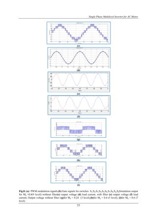
Fig.6: switching angle for each output level
Fig.6 shows the output voltage and switching angle for one cycle.The eight modes are as follows.
Mode1(vs/2) :0<wt<θ1and θ 6<wt<𝝅 Mode2(vs):θ1<wt<θ2andθ5<wt<θ6
Mode3(3vs/2):θ2<wt<θ3and θ 4<wt<θ 5 Mode4(2vs):θ3<wt<θ4
Mode5(-vs/2):𝝅<wt<θ7and θ12<wt<2𝝅 Mode6(-vs):θ7<wt<θ8.andθ11<wt<θ12
Mode7(-3vs/2):θ8<wt<θ 9andθ10<wt<θ 11Mode8(-2vs):θ9<wt<θ 10
Fig.7: SIMULINK model of the proposed circuit with LC filter](https://image.slidesharecdn.com/g09115056-140322024246-phpapp01/85/International-Journal-of-Engineering-Research-and-Development-4-320.jpg)
![Single Phase Multilevel Inverter for AC Motor
54
Generally modulation index [14] is given by Ma =
Ac
Am (k−1)
Where Ac and Amis the amplitude of the carrier signal and reference signal and k the number of
voltage level synthesized per half-cycle. For Ma< 0.25, only lower carrier gets compared with reference signal
and three level output is obtained if 0.25<Ma< 0.5, carriers T1 and T2 are compared and a five level output [10,
13] is obtained. A seven level output is obtained with 0.5< Ma<0.75. When Mavalue is greater than 0.75,a nine
level output is obtained. The gate signals are generated by logic combination of signals generated by comparison
of reference and carrier signal. Also the % THD for different output levels is shown in the Table.II.
IV. SIMULATION RESULTS
The simulation result of proposed PV fed cascaded multilevel inverter topology with and without filter
has been simulated in MATLAB SIMULINK.The proposed inverter is capable of synthesizing 3-,5-,7-,9-levels.
The model of the proposed circuit with filter is shown in fig.7. PWM modulation signals and gate signals for the
switches S1 to S8, SA and SB for a modulation index of 0.8and simulated waveforms of output voltage and
current for an input voltage of 200V (single phase voltage), R=50𝛺, L =50mHfor different modulation index are
obtained as seen in fig.8. The % THD was found and a very small size filter was designed to obtain a %THD of
0.31% for a nine level multilevel inverter and also for three level, five level and seven level inverter %THD was
obtained as 1.88%, 1.7% and 0.4% respectively as shown in Table II.
Table.II: comparison of %THD in output waveforms
Levels Without
Filter(%Thd)
With
Filter(%Thd)
Voltage Current Voltage Current
Three
Level
56.8 16.81 1.88 1.99
Five
Level
38.9 12.36 1.7 1.7
Seven
Level
24.16 7.46 0.40 0.41
Nine
Level
16.97 5.38 0.318 0.307
(a)
(b)](https://image.slidesharecdn.com/g09115056-140322024246-phpapp01/85/International-Journal-of-Engineering-Research-and-Development-5-320.jpg)
![Single Phase Multilevel Inverter for AC Motor
56
V. CONCLUSION
A configuration for multilevel cascaded inverter fed by PV that can be applied to electric drives is
presented in this paper. The working, switching functions and modulation schemes have been analyzed here.
The output voltage and current for circuits with and without filter have been determined. By controlling
modulation index, the desired number of levels in the output has been obtained for both the former circuits. Also
the % THD for each level with and without filter has been determined for each of the desired levels. The
harmonics was greatly reduced to 0.31%with the design of a LC filter and a sinusoidal output at fundamental
frequency was obtained.
REFERENCES
[1]. Meynard, T.A., Foch, H.:„Multi-level conversion: high-voltage chopper and voltage-source inverters‟.
Conf. Rec. 1992 IEEE PESC,1992, pp. 397–403
[2]. T. Esram and P. L. Chapman, “Comparison of Photovoltaic Array Maximum Power Point Tracking
Techniques”, IEEE Transactions on Energy Conversion, Vol. 22, No. 2, pp. 439-449, June 2007.
[3]. D. Sera, R. Teodorescu, J. Hantschel and M. Knoll, “Optimized Maximum Power Point Tracker for
Fast-Changing Environmental Conditions”, IEEE Transactions on Industrial Electronics, Vol. 55, No.
7, pp. 2629-2631, July 2008.
[4]. H. Bodur and A. FarukBakan, “A new ZCT-ZVT-PWM DC–DC converter,” IEEE Trans. Power
Electron.,Vol. 19,No. 3,pp. 676–684,May 2004
[5]. P. K. Hinga, T. Ohnishi, and T. Suzuki, “A new PWM inverter for photovoltaic power generation
system,” in Conf. Rec. IEEE Power Electron. Spec. Conf., 1994, pp. 391–395.
[6]. Charles I. Odeh, Damian B.N. Nnadi“Single-phase 9-level hybridised cascaded multilevel Inverter” on
ET Power Electron., 2013, Vol. 6, Iss. 3, pp. 468–477 doi: 10.1049/iet-pel.2012.0199
[7]. Peng .F.Z.,Lai J.S.,McKeever,J.W., Van Coevering,J.:” a multilevel voltage – source inveterwith
separate DC sources for static VAR generation”,IEEE Trans.Ind.Appl.,1996,32,(5),pp. 1130-1138
[8]. Lezana,P., Rodriguez,J.A.:”Cascaded multilevel inverter with regeneration capability and reduced
number of switches”, IEEE Trans.Ind.Electron.,2008,55,(3),pp. 1059-1066
[9]. Vazquez, s., Leon,J.I.,Carrasco, J.M.et al.:” Analysis of power balance in the cells of a multilevel CHB
converter”,IEEE Trans. Ind. Electron., 2010,57,(7),pp.2287-2296
[10]. Park,S.J., Kang, F-S.,Lee,M.H.,Cheul-U-Kim: “A new single phase, five – level PWM inverter
employing a deadbeat control scheme”, IEEE Trans. Power Electron.,2003,18,(3),pp.831-843
[11]. Grahame Holmes, D., Lipo,T.A.:” Pulse width modulation for power converters,principles and
practice”(John Wiley and Sons, Inc.,Publication, USA, 2003)
[12]. Rahim, N.A., Krismadinata, Selvaraj, J.: „Single-phase, seven-level grid-connected inverter for
photovoltaic system‟, IEEE Trans. Ind.Electron., 2011, 58, (6), pp. 2435– 2443
[13]. Rahim, N.A., Krismadinata, Selvaraj, J.: “Multi-string five level inverter with novel PWM control
scheme for PV application”, IEEE Trans. Ind. Electron., 2010, 58, (6), pp. 2111– 2121
[14]. Sowjanya., K.S.,Naik..M.G.,RamaRao.,J.V.G: ”Design of single phase nine level inverter to drive an
induction motor” IJSR,vol.2.Issue 1.,jan 2013,pg 451.](https://image.slidesharecdn.com/g09115056-140322024246-phpapp01/85/International-Journal-of-Engineering-Research-and-Development-7-320.jpg)

This document summarizes a research paper that proposes a single-phase multilevel inverter topology fed by a photovoltaic panel. The inverter uses a multicarrier phase disposition sinusoidal pulse width modulation scheme to generate gate signals for power switches. It can produce 3, 5, 7, or 9 output voltage levels by controlling the modulation index. The proposed inverter configuration was tested supplying power to an R-L load. Simulation results in MATLAB/Simulink analyzed the performance of the topology and THD values for output current and voltage.


![[IJET-V2I3P17] Authors: R.C.Rohini, G.Srividhya](https://cdn.slidesharecdn.com/ss_thumbnails/ijet-v2i3p17-160711110843-thumbnail.jpg?width=640&height=640&fit=bounds)


![6.[36 45]seven level modified cascaded inverter for induction motor drive app...](https://cdn.slidesharecdn.com/ss_thumbnails/6-36-45sevenlevelmodifiedcascadedinverterforinductionmotordriveapplications-111118182704-phpapp01-thumbnail.jpg?width=640&height=640&fit=bounds)